EP1796107A1 - Conducteur transparent, électrode transparente, cellule solaire, dispositif luminescent et panneau d"affichage - Google Patents
Conducteur transparent, électrode transparente, cellule solaire, dispositif luminescent et panneau d"affichage Download PDFInfo
- Publication number
- EP1796107A1 EP1796107A1 EP05770464A EP05770464A EP1796107A1 EP 1796107 A1 EP1796107 A1 EP 1796107A1 EP 05770464 A EP05770464 A EP 05770464A EP 05770464 A EP05770464 A EP 05770464A EP 1796107 A1 EP1796107 A1 EP 1796107A1
- Authority
- EP
- European Patent Office
- Prior art keywords
- metal oxide
- transparent conductor
- conductor according
- transparent
- tio
- Prior art date
- Legal status (The legal status is an assumption and is not a legal conclusion. Google has not performed a legal analysis and makes no representation as to the accuracy of the status listed.)
- Withdrawn
Links
Images







Classifications
-
- C—CHEMISTRY; METALLURGY
- C03—GLASS; MINERAL OR SLAG WOOL
- C03C—CHEMICAL COMPOSITION OF GLASSES, GLAZES OR VITREOUS ENAMELS; SURFACE TREATMENT OF GLASS; SURFACE TREATMENT OF FIBRES OR FILAMENTS MADE FROM GLASS, MINERALS OR SLAGS; JOINING GLASS TO GLASS OR OTHER MATERIALS
- C03C17/00—Surface treatment of glass, not in the form of fibres or filaments, by coating
- C03C17/22—Surface treatment of glass, not in the form of fibres or filaments, by coating with other inorganic material
- C03C17/23—Oxides
- C03C17/245—Oxides by deposition from the vapour phase
- C03C17/2456—Coating containing TiO2
-
- H—ELECTRICITY
- H01—ELECTRIC ELEMENTS
- H01B—CABLES; CONDUCTORS; INSULATORS; SELECTION OF MATERIALS FOR THEIR CONDUCTIVE, INSULATING OR DIELECTRIC PROPERTIES
- H01B5/00—Non-insulated conductors or conductive bodies characterised by their form
- H01B5/14—Non-insulated conductors or conductive bodies characterised by their form comprising conductive layers or films on insulating-supports
-
- C—CHEMISTRY; METALLURGY
- C03—GLASS; MINERAL OR SLAG WOOL
- C03C—CHEMICAL COMPOSITION OF GLASSES, GLAZES OR VITREOUS ENAMELS; SURFACE TREATMENT OF GLASS; SURFACE TREATMENT OF FIBRES OR FILAMENTS MADE FROM GLASS, MINERALS OR SLAGS; JOINING GLASS TO GLASS OR OTHER MATERIALS
- C03C17/00—Surface treatment of glass, not in the form of fibres or filaments, by coating
- C03C17/34—Surface treatment of glass, not in the form of fibres or filaments, by coating with at least two coatings having different compositions
-
- G—PHYSICS
- G02—OPTICS
- G02F—OPTICAL DEVICES OR ARRANGEMENTS FOR THE CONTROL OF LIGHT BY MODIFICATION OF THE OPTICAL PROPERTIES OF THE MEDIA OF THE ELEMENTS INVOLVED THEREIN; NON-LINEAR OPTICS; FREQUENCY-CHANGING OF LIGHT; OPTICAL LOGIC ELEMENTS; OPTICAL ANALOGUE/DIGITAL CONVERTERS
- G02F1/00—Devices or arrangements for the control of the intensity, colour, phase, polarisation or direction of light arriving from an independent light source, e.g. switching, gating or modulating; Non-linear optics
- G02F1/01—Devices or arrangements for the control of the intensity, colour, phase, polarisation or direction of light arriving from an independent light source, e.g. switching, gating or modulating; Non-linear optics for the control of the intensity, phase, polarisation or colour
- G02F1/13—Devices or arrangements for the control of the intensity, colour, phase, polarisation or direction of light arriving from an independent light source, e.g. switching, gating or modulating; Non-linear optics for the control of the intensity, phase, polarisation or colour based on liquid crystals, e.g. single liquid crystal display cells
- G02F1/133—Constructional arrangements; Operation of liquid crystal cells; Circuit arrangements
- G02F1/1333—Constructional arrangements; Manufacturing methods
- G02F1/1343—Electrodes
-
- G—PHYSICS
- G02—OPTICS
- G02F—OPTICAL DEVICES OR ARRANGEMENTS FOR THE CONTROL OF LIGHT BY MODIFICATION OF THE OPTICAL PROPERTIES OF THE MEDIA OF THE ELEMENTS INVOLVED THEREIN; NON-LINEAR OPTICS; FREQUENCY-CHANGING OF LIGHT; OPTICAL LOGIC ELEMENTS; OPTICAL ANALOGUE/DIGITAL CONVERTERS
- G02F1/00—Devices or arrangements for the control of the intensity, colour, phase, polarisation or direction of light arriving from an independent light source, e.g. switching, gating or modulating; Non-linear optics
- G02F1/01—Devices or arrangements for the control of the intensity, colour, phase, polarisation or direction of light arriving from an independent light source, e.g. switching, gating or modulating; Non-linear optics for the control of the intensity, phase, polarisation or colour
- G02F1/13—Devices or arrangements for the control of the intensity, colour, phase, polarisation or direction of light arriving from an independent light source, e.g. switching, gating or modulating; Non-linear optics for the control of the intensity, phase, polarisation or colour based on liquid crystals, e.g. single liquid crystal display cells
- G02F1/133—Constructional arrangements; Operation of liquid crystal cells; Circuit arrangements
- G02F1/1333—Constructional arrangements; Manufacturing methods
- G02F1/1343—Electrodes
- G02F1/13439—Electrodes characterised by their electrical, optical, physical properties; materials therefor; method of making
-
- H—ELECTRICITY
- H01—ELECTRIC ELEMENTS
- H01B—CABLES; CONDUCTORS; INSULATORS; SELECTION OF MATERIALS FOR THEIR CONDUCTIVE, INSULATING OR DIELECTRIC PROPERTIES
- H01B1/00—Conductors or conductive bodies characterised by the conductive materials; Selection of materials as conductors
- H01B1/06—Conductors or conductive bodies characterised by the conductive materials; Selection of materials as conductors mainly consisting of other non-metallic substances
- H01B1/08—Conductors or conductive bodies characterised by the conductive materials; Selection of materials as conductors mainly consisting of other non-metallic substances oxides
-
- H—ELECTRICITY
- H01—ELECTRIC ELEMENTS
- H01M—PROCESSES OR MEANS, e.g. BATTERIES, FOR THE DIRECT CONVERSION OF CHEMICAL ENERGY INTO ELECTRICAL ENERGY
- H01M14/00—Electrochemical current or voltage generators not provided for in groups H01M6/00 - H01M12/00; Manufacture thereof
- H01M14/005—Photoelectrochemical storage cells
-
- H—ELECTRICITY
- H01—ELECTRIC ELEMENTS
- H01M—PROCESSES OR MEANS, e.g. BATTERIES, FOR THE DIRECT CONVERSION OF CHEMICAL ENERGY INTO ELECTRICAL ENERGY
- H01M4/00—Electrodes
- H01M4/02—Electrodes composed of, or comprising, active material
- H01M4/36—Selection of substances as active materials, active masses, active liquids
- H01M4/48—Selection of substances as active materials, active masses, active liquids of inorganic oxides or hydroxides
-
- H—ELECTRICITY
- H05—ELECTRIC TECHNIQUES NOT OTHERWISE PROVIDED FOR
- H05B—ELECTRIC HEATING; ELECTRIC LIGHT SOURCES NOT OTHERWISE PROVIDED FOR; CIRCUIT ARRANGEMENTS FOR ELECTRIC LIGHT SOURCES, IN GENERAL
- H05B33/00—Electroluminescent light sources
- H05B33/12—Light sources with substantially two-dimensional [2D] radiating surfaces
- H05B33/26—Light sources with substantially two-dimensional [2D] radiating surfaces characterised by the composition or arrangement of the conductive material used as an electrode
- H05B33/28—Light sources with substantially two-dimensional [2D] radiating surfaces characterised by the composition or arrangement of the conductive material used as an electrode of translucent electrodes
-
- H—ELECTRICITY
- H10—SEMICONDUCTOR DEVICES; ELECTRIC SOLID-STATE DEVICES NOT OTHERWISE PROVIDED FOR
- H10F—INORGANIC SEMICONDUCTOR DEVICES SENSITIVE TO INFRARED RADIATION, LIGHT, ELECTROMAGNETIC RADIATION OF SHORTER WAVELENGTH OR CORPUSCULAR RADIATION
- H10F71/00—Manufacture or treatment of devices covered by this subclass
- H10F71/138—Manufacture of transparent electrodes, e.g. transparent conductive oxides [TCO] or indium tin oxide [ITO] electrodes
-
- H—ELECTRICITY
- H10—SEMICONDUCTOR DEVICES; ELECTRIC SOLID-STATE DEVICES NOT OTHERWISE PROVIDED FOR
- H10F—INORGANIC SEMICONDUCTOR DEVICES SENSITIVE TO INFRARED RADIATION, LIGHT, ELECTROMAGNETIC RADIATION OF SHORTER WAVELENGTH OR CORPUSCULAR RADIATION
- H10F77/00—Constructional details of devices covered by this subclass
- H10F77/20—Electrodes
- H10F77/244—Electrodes made of transparent conductive layers, e.g. transparent conductive oxide [TCO] layers
-
- H—ELECTRICITY
- H10—SEMICONDUCTOR DEVICES; ELECTRIC SOLID-STATE DEVICES NOT OTHERWISE PROVIDED FOR
- H10F—INORGANIC SEMICONDUCTOR DEVICES SENSITIVE TO INFRARED RADIATION, LIGHT, ELECTROMAGNETIC RADIATION OF SHORTER WAVELENGTH OR CORPUSCULAR RADIATION
- H10F77/00—Constructional details of devices covered by this subclass
- H10F77/20—Electrodes
- H10F77/244—Electrodes made of transparent conductive layers, e.g. transparent conductive oxide [TCO] layers
- H10F77/247—Electrodes made of transparent conductive layers, e.g. transparent conductive oxide [TCO] layers comprising indium tin oxide [ITO]
-
- H—ELECTRICITY
- H10—SEMICONDUCTOR DEVICES; ELECTRIC SOLID-STATE DEVICES NOT OTHERWISE PROVIDED FOR
- H10F—INORGANIC SEMICONDUCTOR DEVICES SENSITIVE TO INFRARED RADIATION, LIGHT, ELECTROMAGNETIC RADIATION OF SHORTER WAVELENGTH OR CORPUSCULAR RADIATION
- H10F77/00—Constructional details of devices covered by this subclass
- H10F77/20—Electrodes
- H10F77/244—Electrodes made of transparent conductive layers, e.g. transparent conductive oxide [TCO] layers
- H10F77/251—Electrodes made of transparent conductive layers, e.g. transparent conductive oxide [TCO] layers comprising zinc oxide [ZnO]
-
- C—CHEMISTRY; METALLURGY
- C03—GLASS; MINERAL OR SLAG WOOL
- C03C—CHEMICAL COMPOSITION OF GLASSES, GLAZES OR VITREOUS ENAMELS; SURFACE TREATMENT OF GLASS; SURFACE TREATMENT OF FIBRES OR FILAMENTS MADE FROM GLASS, MINERALS OR SLAGS; JOINING GLASS TO GLASS OR OTHER MATERIALS
- C03C2217/00—Coatings on glass
- C03C2217/20—Materials for coating a single layer on glass
- C03C2217/21—Oxides
- C03C2217/212—TiO2
-
- C—CHEMISTRY; METALLURGY
- C03—GLASS; MINERAL OR SLAG WOOL
- C03C—CHEMICAL COMPOSITION OF GLASSES, GLAZES OR VITREOUS ENAMELS; SURFACE TREATMENT OF GLASS; SURFACE TREATMENT OF FIBRES OR FILAMENTS MADE FROM GLASS, MINERALS OR SLAGS; JOINING GLASS TO GLASS OR OTHER MATERIALS
- C03C2217/00—Coatings on glass
- C03C2217/20—Materials for coating a single layer on glass
- C03C2217/21—Oxides
- C03C2217/218—V2O5, Nb2O5, Ta2O5
-
- C—CHEMISTRY; METALLURGY
- C03—GLASS; MINERAL OR SLAG WOOL
- C03C—CHEMICAL COMPOSITION OF GLASSES, GLAZES OR VITREOUS ENAMELS; SURFACE TREATMENT OF GLASS; SURFACE TREATMENT OF FIBRES OR FILAMENTS MADE FROM GLASS, MINERALS OR SLAGS; JOINING GLASS TO GLASS OR OTHER MATERIALS
- C03C2217/00—Coatings on glass
- C03C2217/20—Materials for coating a single layer on glass
- C03C2217/21—Oxides
- C03C2217/23—Mixtures
-
- C—CHEMISTRY; METALLURGY
- C03—GLASS; MINERAL OR SLAG WOOL
- C03C—CHEMICAL COMPOSITION OF GLASSES, GLAZES OR VITREOUS ENAMELS; SURFACE TREATMENT OF GLASS; SURFACE TREATMENT OF FIBRES OR FILAMENTS MADE FROM GLASS, MINERALS OR SLAGS; JOINING GLASS TO GLASS OR OTHER MATERIALS
- C03C2217/00—Coatings on glass
- C03C2217/20—Materials for coating a single layer on glass
- C03C2217/21—Oxides
- C03C2217/24—Doped oxides
-
- C—CHEMISTRY; METALLURGY
- C03—GLASS; MINERAL OR SLAG WOOL
- C03C—CHEMICAL COMPOSITION OF GLASSES, GLAZES OR VITREOUS ENAMELS; SURFACE TREATMENT OF GLASS; SURFACE TREATMENT OF FIBRES OR FILAMENTS MADE FROM GLASS, MINERALS OR SLAGS; JOINING GLASS TO GLASS OR OTHER MATERIALS
- C03C2218/00—Methods for coating glass
- C03C2218/10—Deposition methods
- C03C2218/15—Deposition methods from the vapour phase
-
- G—PHYSICS
- G02—OPTICS
- G02F—OPTICAL DEVICES OR ARRANGEMENTS FOR THE CONTROL OF LIGHT BY MODIFICATION OF THE OPTICAL PROPERTIES OF THE MEDIA OF THE ELEMENTS INVOLVED THEREIN; NON-LINEAR OPTICS; FREQUENCY-CHANGING OF LIGHT; OPTICAL LOGIC ELEMENTS; OPTICAL ANALOGUE/DIGITAL CONVERTERS
- G02F2201/00—Constructional arrangements not provided for in groups G02F1/00 - G02F7/00
- G02F2201/12—Constructional arrangements not provided for in groups G02F1/00 - G02F7/00 electrode
-
- G—PHYSICS
- G02—OPTICS
- G02F—OPTICAL DEVICES OR ARRANGEMENTS FOR THE CONTROL OF LIGHT BY MODIFICATION OF THE OPTICAL PROPERTIES OF THE MEDIA OF THE ELEMENTS INVOLVED THEREIN; NON-LINEAR OPTICS; FREQUENCY-CHANGING OF LIGHT; OPTICAL LOGIC ELEMENTS; OPTICAL ANALOGUE/DIGITAL CONVERTERS
- G02F2202/00—Materials and properties
- G02F2202/06—Materials and properties dopant
-
- G—PHYSICS
- G02—OPTICS
- G02F—OPTICAL DEVICES OR ARRANGEMENTS FOR THE CONTROL OF LIGHT BY MODIFICATION OF THE OPTICAL PROPERTIES OF THE MEDIA OF THE ELEMENTS INVOLVED THEREIN; NON-LINEAR OPTICS; FREQUENCY-CHANGING OF LIGHT; OPTICAL LOGIC ELEMENTS; OPTICAL ANALOGUE/DIGITAL CONVERTERS
- G02F2203/00—Function characteristic
- G02F2203/01—Function characteristic transmissive
-
- Y—GENERAL TAGGING OF NEW TECHNOLOGICAL DEVELOPMENTS; GENERAL TAGGING OF CROSS-SECTIONAL TECHNOLOGIES SPANNING OVER SEVERAL SECTIONS OF THE IPC; TECHNICAL SUBJECTS COVERED BY FORMER USPC CROSS-REFERENCE ART COLLECTIONS [XRACs] AND DIGESTS
- Y02—TECHNOLOGIES OR APPLICATIONS FOR MITIGATION OR ADAPTATION AGAINST CLIMATE CHANGE
- Y02E—REDUCTION OF GREENHOUSE GAS [GHG] EMISSIONS, RELATED TO ENERGY GENERATION, TRANSMISSION OR DISTRIBUTION
- Y02E10/00—Energy generation through renewable energy sources
- Y02E10/50—Photovoltaic [PV] energy
-
- Y—GENERAL TAGGING OF NEW TECHNOLOGICAL DEVELOPMENTS; GENERAL TAGGING OF CROSS-SECTIONAL TECHNOLOGIES SPANNING OVER SEVERAL SECTIONS OF THE IPC; TECHNICAL SUBJECTS COVERED BY FORMER USPC CROSS-REFERENCE ART COLLECTIONS [XRACs] AND DIGESTS
- Y02—TECHNOLOGIES OR APPLICATIONS FOR MITIGATION OR ADAPTATION AGAINST CLIMATE CHANGE
- Y02E—REDUCTION OF GREENHOUSE GAS [GHG] EMISSIONS, RELATED TO ENERGY GENERATION, TRANSMISSION OR DISTRIBUTION
- Y02E60/00—Enabling technologies; Technologies with a potential or indirect contribution to GHG emissions mitigation
- Y02E60/10—Energy storage using batteries
-
- Y—GENERAL TAGGING OF NEW TECHNOLOGICAL DEVELOPMENTS; GENERAL TAGGING OF CROSS-SECTIONAL TECHNOLOGIES SPANNING OVER SEVERAL SECTIONS OF THE IPC; TECHNICAL SUBJECTS COVERED BY FORMER USPC CROSS-REFERENCE ART COLLECTIONS [XRACs] AND DIGESTS
- Y10—TECHNICAL SUBJECTS COVERED BY FORMER USPC
- Y10T—TECHNICAL SUBJECTS COVERED BY FORMER US CLASSIFICATION
- Y10T428/00—Stock material or miscellaneous articles
- Y10T428/12—All metal or with adjacent metals
- Y10T428/12493—Composite; i.e., plural, adjacent, spatially distinct metal components [e.g., layers, joint, etc.]
- Y10T428/1266—O, S, or organic compound in metal component
- Y10T428/12667—Oxide of transition metal or Al
Definitions
- the present invention relates to a transparent conductor to be applied for a liquid crystal panel, a solar cell, an organic electroluminescence (EL) electrode, and the like.
- an organic electroluminescence (EL) device developed recently is a self-luminous type device and can be effectively applied to a small portable device, however, there are problems in which the organic EL device is a current driven device and has a large power consumption.
- a plasma display panel (PDP) which is spreading in the market recently and a field emission display (FED) currently developed as a next-generation display have a problem in that they have high power consumption structures. Therefore, a low resistance-transparent conductive thin film is greatly expected.
- the transparent conductive thin film in which an indium tin oxide film (hereinafter referred to as ITO film) consisting of indium oxide doped with tin within a certain percentage is provided on the surface of a transparent substrate such as a glass plate or the like is proposed (for example, patent document 1).
- the ITO film has superior transparency and high conductivity, however, there are problems that the content of indium in the earth crust is very low 50 ppb and the cost of raw materials increases as resources are exhausted.
- the zinc oxide material is weak to acid or alkali, and is gradually eroded in a carbon dioxide atmosphere, particularly, application to a solar cell becomes difficult as well as application to a liquid crystal panel. Even if it is considered that the surface of the zinc oxide is treated by a coating process in order to improve the chemical resistance, adding a process for coating causes an increase in production cost.
- Patent Document 1 Japanese Unexamined Patent Application, First Publication 2004-095240
- the present invention was made in view of the above-described background technology. Its object is to provide a transparent conductor having transparency and conductivity which is capable of being stably supplied and is composed of raw materials with superior chemical resistance.
- the first aspect of the present invention is a transparent conductor including a metal oxide characterized in that the metal oxide is M:TiO 2 having an anatase type crystal structure.
- the second aspect of the present invention is a transparent conductor including a metal oxide characterized in that the metal oxide is a M:TiO 2 having an anatase type crystal structure (M is one selected from the group consisting ofNb, Ta, Mo, As, Sb and W).
- M is one selected from the group consisting ofNb, Ta, Mo, As, Sb and W.
- the third aspect of the present invention is a transparent conductor including a metal oxide characterized in that the metal oxide is a M:TiO 2 having an anatase type crystal structure (M is one selected from the group consisting of V, Mn, Tc, Re, P, and Bi).
- M is one selected from the group consisting of V, Mn, Tc, Re, P, and Bi.
- the fourth aspect of the present invention is a transparent conductor including a metal oxide characterized in that the metal oxide is a M:TiO 2 having an anatase type crystal structure (M is one selected from the group consisting ofTa and Nb).
- the fifth aspect of the present invention is a transparent conductor according to the first aspect characterized in that the metal oxide also has metallic electric conductivity.
- the sixth aspect of the present invention is a transparent conductor according to the fourth aspect characterized in that the metal oxide is represented by the formula Ti 1-x Nb x O 2 (0.001 ⁇ x ⁇ 0.2).
- the seventh aspect of the present invention is a transparent conductor according to the fourth aspect characterized in that the metal oxide is represented by the formula Ti 1-x Nb x O 2 (0.01 ⁇ x ⁇ 0.2).
- the eighth aspect of the present invention is a transparent conductor according to the fourth aspect characterized in that the metal oxide is represented by the formula Ti 1-x Nb x O 2 (0.01 ⁇ x ⁇ 0.03).
- the ninth aspect of the present invention is a transparent conductor according to the fourth aspect characterized in that the metal oxide is represented by the formula Ti 1-x Nb x O 2 (0.01 ⁇ x ⁇ 0.6).
- the tenth aspect of the present invention is a transparent conductor according to the fourth aspect characterized in that the metal oxide is represented by the formula Ti 1-x Nb x O 2 (0.02 ⁇ x ⁇ 0.6).
- the eleventh aspect of the present invention is a transparent conductor according to the fourth aspect characterized in that the metal oxide is represented by the formula Ti 1-x Ta x O 2 (0.001 ⁇ x ⁇ 0.2).
- the twelfth aspect of the present invention is a transparent conductor according to the fourth aspect characterized in that the metal oxide is represented by the formula Ti 1-x Ta x O 2 (0.005 ⁇ x ⁇ 0.2).
- the thirteenth aspect of the present invention is a transparent conductor according to the fourth aspect characterized in that the metal oxide is represented by the formula Ti 1-x Ta x O 2 (0.01 ⁇ x ⁇ 0.1).
- the fourteenth aspect of the present invention is a transparent conductor according to the fourth aspect characterized in that the metal oxide is represented by the formula Ti 1-x Ta x O 2 (0.03 ⁇ x ⁇ 0.1).
- the fifteenth aspect of the present invention is a transparent conductor according to the fourth aspect characterized in that the metal oxide is represented by the formula Ti 1-x Ta x O 2 (0.05 ⁇ x ⁇ 0.1).
- the sixteenth aspect of the present invention is a transparent conductor according to the fourth aspect characterized in that the metal oxide is represented by the formula Ti 1-x-y Nb x Ta y O 2 (0 ⁇ x+y ⁇ 0.4).
- the seventeenth aspect of the present invention is a transparent conductor according to the fourth aspect characterized in that the metal oxide is represented by the formula Ti 1-x-y Nb x Ta y O 2 (0 ⁇ x+y ⁇ 0.3).
- the eighteenth aspect of the present invention is the transparent conductor according to the first aspect characterized in that the metal oxide is provided on a perovskite type crystal substrate.
- the nineteenth aspect of the present invention is the transparent conductor according to the fourth aspect characterized in that the metal oxide has resistivity of 2 ⁇ 10 -4 to 5 ⁇ 10 -4 ⁇ cm at room temperature or 8 ⁇ 10 -5 to 2 ⁇ 10 -4 ⁇ cm at cryogenic temperature.
- the twentieth aspect of the present invention is the transparent conductor according to the fourth aspect characterized in that the metal oxide has resistivity of 2 ⁇ 10 -4 to 1.8 ⁇ 10 -3 ⁇ cm at room temperature or 5 ⁇ 10 -5 to 7 ⁇ 10 -4 ⁇ cm at cryogenic temperature.
- the twenty-first aspect of the present invention is a transparent electrode comprising the transparent conductor according to the first aspect.
- the twenty-second aspect of the present invention is the transparent conductor according to the first aspect characterized in that the metal oxide is provided to a GaN compound film.
- the twenty-third aspect of the present invention is the transparent conductor according to the first aspect characterized in that the metal oxide is provided to an oriented film which is provided to a substrate.
- the twenty-fourth aspect of the present invention is the transparent conductor according to the twenty-third aspect characterized in that the oriented film is at least one selected from the group consisting of ZnO, ZrO 2 , SrTiO 3 , MgO, LaAlO 3 , CeO 2 , ZrO 2 , and Al 2 O 3 films.
- the twenty-fifth aspect of the present invention is the transparent conductor according to the twenty-third aspect characterized in that the oriented film is a ZnO film.
- the twenty-sixth aspect of the present invention is the transparent conductor according to the first aspect characterized in that a d electron imparts electric conductivity.
- the twenty-seventh aspect of the present invention is a solar cell comprising the transparent conductor according to the first aspect.
- the twenty-eighth aspect of the present invention is a light emitting device comprising the transparent conductor according to the first aspect.
- the twenty-ninth aspect of the present invention is a display panel comprising the transparent conductor according to the first aspect.
- the present invention enables a remarkable increase of the electric conductivity while maintaining the transparency by using M:TiO 2 obtained by replacing Ti site of an anatase type TiO 2 with another metal atom (Nb, Ta, Mo, As, Sb, W, or the like) or the like.
- the crystalline form of the M:TiO 2 may a single crystal or a polycrystal,
- the Nb substitution is 0.1 to 20% as the ratio of the number of Nb and Ti atoms (Nb/Ti) in the metal oxide, it becomes possible to suppress the resistivity to a level of 10 -4 ⁇ cm.
- the Nb substitution is 1 to 20% as the ratio of the number of Nb and Ti atoms (Nb/Ti) in the metal oxide, it becomes possible to suppress the resistivity to a level of 10 -4 ⁇ cm while the internal transmittance is maintained at a high level.
- the Nb substitution is 1 to 6% as the ratio of the number ofNb and Ti atoms (Nb/Ti) in the metal oxide, it becomes possible to improve the internal transmittance to 95 to 98% (when the metal oxide is formed to a thin film as a sample and the thickness of the film is approximately 50 nm).
- the Nb substitution is 2 to 6% as the ratio of the number of Nb and Ti atoms (Nb/Ti) in the metal oxide, it becomes possible to suppress the resistivity to approximately 5 ⁇ 10 -4 ⁇ cm at room temperature and 1 ⁇ 10 -4 ⁇ cm at cryogenic temperature (approximately 5K) while the internal transmittance is further improved,
- the Ta substitution is 0.1 to 20% as the ratio of the number of Ta and Ti atoms (Ta/Ti) in the metal oxide, it becomes possible to suppress the resistivity to a level between 10 -4 ⁇ cm and 10 -3 ⁇ cm.
- the Ta substitution is 0.5 to 20% as the ratio of the number of Ta and Ti atoms (Ta/Ti) in the metal oxide, it becomes possible to suppress the resistivity to a level between 10 -4 ⁇ cm and 10 -3 ⁇ cm while the internal transmittance is maintained at a high level.
- the Ta substitution is 1 to 5% as the ratio of the number of Ta and Ti atoms (Ta/Ti) in the metal oxide, it becomes possible to stably obtain high internal transmittance even if red light is used.
- the Ta substitution is 1 to 3% as the ratio of the number of Ta and Ti atoms (Ta/Ti) in the metal oxide, it becomes possible to suppress the resistivity to approximately 5 ⁇ 10 -4 ⁇ cm at room temperature and 1 ⁇ 10 -4 to 2 ⁇ 10 -4 ⁇ cm at cryogenic temperature while high internal transmittance is stably obtained even if red light is used.
- the resistivity of the metal oxide By setting the resistivity of the metal oxide to 2 ⁇ 10 -4 to 5 ⁇ 10 -4 ⁇ cm at room temperature or 8 ⁇ 10 -5 to 2 ⁇ 10 -4 ⁇ cm at cryogenic temperature, or to 3 ⁇ 10 -4 to 1.8 ⁇ 10 -3 ⁇ cm at room temperature or 5 ⁇ 10 -5 to 7 ⁇ 10 -4 ⁇ cm at cryogenic temperature, it becomes possible to remarkably extend applicability for various devices such as a display panel. According to the present invention, particularly, enlargement of area and mass production of the transparent conductor are carried out using the TiO 2 film deposition technique.
- a substrate for transparent electrodes is able to be applied to an electrode for a solar cell which uses TiO 2 as a photocatalyst in addition to application for an electrode of a conventional solar cell.
- Applying the substrate for transparent electrodes to a liquid crystal display panel causes a reduction of the power consumption of a display device of the liquid crystal display panel, and therefore, enlargement and miniaturization for portability of the liquid crystal display panel are accelerated.
- the labor accompanying production is remarkably reduced in addition to cost reduction with facilitation of raw material acquisition and simplification of production processes.
- TiO 2 having high durability to chemicals and outside air is used as a parent material in the present invention, it becomes possible to extend applicability to solar cells to be expected with the usage in field. Furthermore, since a coating process is not required, cost reduction with a decrease of the number of processes is achieved.
- the present invention is applied for use as a transparent metal (transparent conductor) 1 to be applied to electrodes of display panels, organic ELs, solar cells, or the like.
- the present invention comprises a metal oxide layer 12 formed on a substrate 11 as a polycrystal or single crystal as shown in Fig. 1.
- the transparent metal 1 shows metallic electric conductivity in the transparent conductor until the cryogenic temperature (5K) in which the metallic electric conductivity is defined to have 10 -2 ⁇ cm or less of resistivity at room temperature and dR/dT > 0 (R: resistivity, T: temperature) of temperature dependency of resistivity.
- the metallic electric conductivity preferably has 10 -3 ⁇ cm or less resistivity at room temperature in view of increasing general use.
- the substrate 11 is composed of strontium titanate (SrTiO 3 ) formed so that a substrate surface 11a is a (100) plane.
- the substrate 11 may be composed of a SrTiO 3 single crystal substrate, or may be composed of any material as long as the material is another perovskite type crystal or a rock type crystal containing similar structure thereto. That is, when the substrate 11 is composed of perovskite type or rock type crystal, an anatase single crystal thin layer can be formed.
- the substrate 11 may be composed of an amorphous material such as glass, quartz, or plastic.
- an anatase polycrystal thin layer is formed, however, it hardly affects fundamental physical properties such as resistivity.
- the thickness of the substrate 11 is not limited to 50 nm, as described in the following embodiment, the thickness is, for example, preferably 1000 nm or less. The thickness may be greater than 1000 nm if substrate 11 is required to have lower resistance and is allowed to have slightly lower transmittance.
- the metal oxide layer 12 formed by laminating on the substrate 11 is composed of Nb:TiO 2 .
- Nb:TiO 2 is formed by substituting Nb for Ti of the anatase TiO 2 .
- Nb may be replaced with, for example, Ta, Mo, As, Sb, or W. Another element may also be used.
- the metal oxide layer 12 is formed on a substrate surface 12a with epitaxial growth.
- the thickness of the metal oxide layer 12 is preferably 40 to 50 nm, however, the thickness is not limited to this range.
- a SrTiO 3 substrate which is cut so that the substrate surface becomes a (100) plane is mechanically polished using, for example, a diamond slurry.
- the particle size of the diamond slurry used is gradually made finer and lastly, mirror polishing is carried out with approximately 0.5 ⁇ m of the particle size of the diamond slurry.
- the surface of SrTiO 3 substrate may be flattened by further polishing with colloidal silica until the RMS of the surface roughness becomes 10 ⁇ or less.
- Nb:TiO 2 is deposited on the SrTiO 3 (100) plane of the substrate 11 by a physical vapor deposition (PVD) process.
- PVD physical vapor deposition
- PLD pulsed laser deposition
- the metal oxide layer 12 is deposited on the substrate 11 using a PLD device 30 as shown in Fig. 2.
- the PLD device 30 comprises a chamber 31, the substrate 11 and a target 39 provided in the chamber 31, a light emitter 32 which is provided opposite to the surface of the target 39 outside the chamber 31, a reflecting mirror 33 for adjusting the position of a pulsed laser light emitted from the light emitter 32 provided outside the chamber 31, a lens 34 for controlling a spot diameter of a laser beam provided outside the chamber 31, and a gas supply device 44 for injecting oxygen gas into the chamber 31 provided outside the chamber 31.
- the chamber 31 is provided for preparing a high quality thin film by maintaining an appropriate degree of vacuum and, concurrently, by preventing contamination from the outside.
- an infrared lump 36 is provided for heating a substrate.
- the temperature of substrate is monitored by a radiation thermometer 37 provided outside the chamber 31 via a window 31b and is controlled so as to always be a constant temperature, Furthermore, a valve 45 for regulating the flow rate of oxygen gas is provided in the chamber 31.
- the chamber 31 is connected with a turbo molecular pump 42 and a pressure valve 43.
- the pressure of the chamber 31 is controlled by the oxygen gas flow rate regulating valve 45 and the pressure valve 43 so as to be 10 -5 to 1 ⁇ 10 -4 torr in, for example, an oxygen atmosphere.
- the turbo molecular pump 42 is connected with an oil-sealed rotary pump 40 and a back-flow preventing valve 41 and the pressure at the exhaust side of the turbo molecular pump 42 is always maintained so as to be 10 -4 torr or less.
- a window 31 a is further provided at the surface of the chamber 31 which is opposite to the target 39.
- the light emitter 32 emits the pulsed laser light incident on the chamber 31 via the window 31a.
- the light emitter 32 emits a KrF excimer laser having, for example, 1 to 10 Hz of pulse frequency, 50 mJ/pulse of laser power, and 248 nm of wavelength as the above-described pulsed laser light.
- the emitted pulsed laser light is spot-adjusted so that the focal position is near the target 39 by the reflecting mirror 33 and the lens 34, and incidence is carried out at an angle of approximately 45° to the surface of the target 39 provided in the chamber 31 via the window 31a.
- the target 39 is composed of, for example, a Nb:TiO 2 sintered body.
- the metal to be substituted is Nb as an example in this embodiment, however, any one of Ta, Mo, As, Sb, and W may be used or plural kinds of metals may be combined.
- the Nb:TiO 2 sintered body is prepared by mixing TiO 2 powder and Nb 2 O 5 powder which are weighed so as to be a desired atomic ratio and further heat-molding the mixed powder.
- the target 39 is provided to be parallel to the (100) plane of the substrate 11.
- the substrate 11 which is polished is provided in the chamber 31.
- the substrate 11 is annealed under an oxygen atmosphere of 10 -5 Torr at 650°C substrate temperature in order to remove impurities on the surface of the substrate 11 and flatten the surface at an atomic level. At least one hour is required as the annealing time.
- the substrate 11 is driven with rotation by motor 35 under an oxygen atmosphere 10 -5 Torr at 550°C of substrate temperature to deposit a film.
- the above-described pulsed laser light is intermittently irradiated to the target 39 while the target 39 is driven with rotation via a rotation axis 38, and thereby the surface temperature of the target 39 is rapidly increased and ablation plasma is generated.
- Each atom of Ti, Nb, and O included in the ablation plasma migrates to the substrate 11 while gradually changing conditions by repeating the collisional reaction or the like with oxygen gas in the chamber 31.
- Particles including Ti, Nb, or O atoms arrived at the substrate 11 diffuse the (100) plane on the substrate 11 as it is, and a thin film is formed in the stablest condition in lattice matching.
- the transparent metal 1 composed of the above-described constitution is prepared.
- the transparent metal 1 may be prepared by not only the PLD method described above but also, for example, other physical vapor deposition (PVD) methods such as a molecular beam epitaxy method (MBE), a sputtering method, and the like, or a method other than PLD methods such as chemical vapor deposition (CVD) methods using, for example, an MOCVD method.
- PVD physical vapor deposition
- MBE molecular beam epitaxy method
- CVD chemical vapor deposition
- MOCVD metal vapor deposition
- the transparent metal 1 may also be prepared by a synthetic process from a solution such as a sol-gel method, a chemical solution method, and the like.
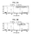
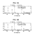
- X-ray diffraction (XRD) measurement of the metal oxide layer 12 was carried out when the Nb substitutional rate x was 0, 0.01, 0.02, and 0.03 in the transparent metal Nb:TiO 2 (chemical formula Ti 1-x Nb x O 2 ) prepared based on the above-described methods. The results are shown in Figs. 3A, 3B, 4A, and 4B. Similarly, an X-ray diffraction (XRD) measurement of the metal oxide layer 12 was carried out when the Nb substitutional rate x was changed with 0.06, 0.1, 0.15, and 0.2 in the transparent metal Nb:TiO 2 (chemical formula Ti 1-x Nb x O 2 ) prepared based on the above-described methods.
- the relationship of lattice constant and the Nb substitutional rate x in the prepared metal oxide layer 12 was determined based on XRD spectrums when the Nb substitutional rate x was 0, 0.01, 0.02, 0.03, 0.06, 0.1, 0,15, and 0.20. It is found that the lattice constant increases as the rate of addition of Nb increases. This result suggests that the prepared metal oxide layer 12 exists as what is known as a solid solution.
- the internal transmittance of the prepared metal oxide layer 12 when the Nb substitutional rate x was 0, 0.01, 0.02, 0.03, 0.06, 0.1, 0.15, and 0.2 was determined.
- the "transmittance" in an original meaning must consider that the amount of reflection is a deficiency, and then, when the amount of reflection in the metal oxide layer 12 is deducted, the transmittance used as 100% is hereinafter referred to "internal transmittance".
- the result is shown in Fig. 8. As shown in Fig. 8, the internal transmittance is 80% or greater in the visible light region (400 to 800 nm of wavelength) which is a satisfactory result.
- a sample having the Nb substitutional rate x being 0.06 or less made it possible to achieve internal transmittance being 95% or greater in the visible light region.
- the cause by which internal transmittance decreases as the Nb substitutional rate increases it is considered that the amount of Ti 3+ as well as Nb substitutional rate increase and transition probability between t 2g -e g bands each having an absorption edge in the visible light region increases.
- the thickness of the metal oxide layer 12 is 100 nm or greater in many cases, and especially, the specifications required in ITO now is 80% or greater internal transmittance to the film thickness 100nm or greater. 95% or greater internal transmittance to the film thickness 50nm is required for satisfying the specifications.
- a transparent conductor thin film which has higher internal transmittance than that of the conventional ITO thin film can be prepared.
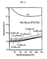
- Fig. 9 shows the temperature dependency of the resistivity of the metal oxide layer 12 prepared with the above-described Nb substitutional rate.
- the metal oxide layer 12 in which the Nb substitutional rate x is 0.01 or greater and 0.2 or less has satisfactory conductivity at a level of 10 -4 ⁇ cm at room temperature in comparison with a metal oxide layer having no Nb.
- the present invention makes it possible that the transparent metal 1 according to the present invention has resistivity at a level of 10 -4 ⁇ cm when the Nb substitutional rate x is not only 0.01 or greater and 0.2 or less but is also 0,001 or greater and 0.2 or less.
- resistivity is decreased to 5 ⁇ 10 -4 ⁇ cm at room temperature (280 to 300K) and 1 ⁇ 10 -4 ⁇ cm at cryogenic temperature (5 to 20K) while internal transmittance is further improved.
- the present invention makes it possible that the transparent metal 1 according to the present invention has high transparency and low resistivity (conductivity at a level of 10 -4 ⁇ cm) almost equal to that of the ITO film in which Nb:TiO 2 obtained by substituting Nb for Ti of the anatase TiO 2 is used as the metal oxide layer 12.
- the Nb substitutional ratio of the metal oxide layer 12 is controlled so that the resistivity of the metal oxide layer 12 becomes 2 ⁇ 10 - 4 to 5 ⁇ 10 -4 ⁇ cm at room temperature or 8 ⁇ 10 -5 to 2 ⁇ 10 -4 ⁇ cm at cryogenic temperature, it becomes possible to remarkably extend applicability to various devices such as a liquid crystal panel.
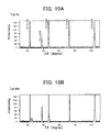
- the X-ray diffraction (XRD) measurement of the metal oxide layer 12 was carried out when the Ta substitutional rate x was 0.002, 0.005, 0.15, and 0.20 in the transparent metal Ta:TiO 2 (chemical formula Ti 1-x Ta x O 2 ) prepared based on the above-described methods.
- the results are shown in Figs. 10A, 10B, 11A, and 11B. According to the XRD spectrums shown in Figs. 10A to 11B, these results confirmed that Ta:TiO 2 is stably generated without depending on the Ta substitutional rate like Nb:TiO 2 .
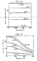
- Fig. 12 is a diagram showing a measurement result of temperature variations of carrier concentrations. Carrier concentrations were determined when the Ta substitutional rate was 0.005, 0.1, 0.03, 0.05, and 0.10. As shown in Fig. 12, the temperature dependency of the carrier concentration in any Ta substitutional rate did not appear. This means that Ta:TiO 2 is a degenerated semiconductor which is a property appearing in a transparent conductive film such as an ITO film.
- Fig. 13 is a diagram showing a measurement result of temperature variations of Hall mobilities. Hall mobilities were determined when the Ta substitutional rate was 0,005, 0.1, 0.03, 0.05, and 0.10. As shown in Fig, 13, Hall mobilities decreased with a temperature rise in any Ta substitutional rate, and reduction of Hall mobility became large as the Ta substitutional rate became small.
- the temperature dependency of Hall mobility is a property which is not observed in ITO, and that causes an increase of resistivity with a temperature rise. The derivation of temperature dependency is not clear now, however, an increase of resistivity with the temperature rise is a property which is observed in ordinary metals and thereby Ta:TiO 2 is called a transparent metal.
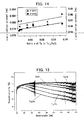
- the relationship of the lattice constant and the Ta substitutional rate x in the prepared metal oxide layer 12 was determined based on the XRD spectrum when the Nb substitutional rate x was 0.005, 0.1, 0.05, 0.10, 0.15, and 0.20. As shown in Fig. 14, it is found that lattice constant increases as the rate of addition ofNb increases, that is, it is found that lattice expands in accordance with Vegard's law (the linear relationship between the lattice constant and the composition of a solid solution alloy expressed with weight percentage). This result suggests that the prepared metal oxide layer 12 exists as what is known as a solid solution. In Fig. 14, triangles represent a-axis lattice constants and circles represent c-axis lattice constants.
- the transmittance of the metal oxide layer 12 prepared when the Ta substitutional rate x was 0.01, 0.03, 0.05, 0.10, 0.15, and 0.20 was determined. The result is shown in Fig. 15. As shown in Fig. 15, the transmittance is 60% or greater in the visible light region (400 to 800 nm of wavelength) which is a satisfactory result. In particular, a sample having the Ta substitutional rate x being 0.05 or less made it possible to achieve stable and high transmittance even if in the visible light long-wavelength region (red region).
- Fig. 16 shows the temperature dependency of the resistivity of the metal oxide layer 12 prepared with the above-described Ta substitutional rate.
- the metal oxide layer 12 in which the Ta substitutional rate x is 0.005 or greater and 0.2 or less has satisfactory conductivity at a level between 10 -4 ⁇ cm and 10 -3 ⁇ cm at room temperature.
- the Ta substitutional rate x is preferably 0.01 or greater and 0.1 or less.
- the Ta substitutional rate x is more preferably 0.03 or greater and 0.1 or less.
- Fig. 17 is a diagram showing the relationship of the amount of Ta doped and the resistivity/transmittance
- circles represent the resistivities and triangles represent the transmittances.
- a region being of small resistivity and large transmittance is the region of the Ta substitutional rate x being 0,03 or greater and 0.1 or less.
- a region being of smaller resistivity and larger transmittance is the region of Ta substitutional rate x being 0.05 or greater and 0.1 or less.
- the present invention makes it possible that the transparent metal 1 according to the present invention has resistivity at a level between 10 -4 ⁇ cm and 10 -3 ⁇ cm when the Ta substitutional rate x is not only 0.005 or greater and 0.2 or less but is also 0.001 or greater and 0.2 or less.
- the Ta substitutional rate x is 0.01 or greater and 0.05 or less in the metal oxide layer 12, stable and high transmittance is able to be achieved even if in the red region.
- resistivity is decreased to 5 ⁇ 10 -4 ⁇ cm at room temperature (280 to 300K) and 5 ⁇ 10 -5 to 2 ⁇ 10 -4 ⁇ cm at cryogenic temperature (5 to 20K) while stable and high transmittance is achieved even if in the red region.
- the present invention makes it possible that the transparent metal 1 according to the present invention has a high transparency and low resistivity almost equal to that of the ITO film in which Ta:TiO 2 obtained by substituting Ta for Ti of the anatase TiO 2 is used as the metal oxide layer 12.
- the Ta substitutional ratio of the metal oxide layer 12 is controlled so that the resistivity of the metal oxide layer 12 becomes 2 ⁇ 10 -4 to 1.8 ⁇ 10 -3 ⁇ cm at room temperature or 5 ⁇ 10 -5 to 7 ⁇ 10 -4 ⁇ cm at cryogenic temperature, it becomes possible to remarkably extend applicability to various devices such as a liquid crystal panel.
- transparent metal 1 can be applied to an electrode for a solar cell which uses TiO 2 as a photocatalyst in addition to application for an electrode of a conventional solar cell.
- Applying the transparent metal I having a low resistivity to a liquid crystal display panel causes reduction of the power consumption of the display device of the liquid crystal display panel, and therefore, enlargement and miniaturization for portability of the liquid crystal display panel can be accelerated. According to the above-described constitution, labor accompanying production is remarkably reduced in addition to cost reduction with facilitation of raw material acquisition and simplification of production processes using the transparent metal 1.
- the transparent metal 1 according to the present invention when used as an electrode, a transparent electrode having conventional performance can be produced at a low price and thereby applicability can be extended. Furthermore, since Nb:TiO 2 , Ta:TiO 2 , and the like which are not eroded by acid and alkali are used as the metal oxide layer 12 constituting the transparent metal 1, applicability can be extended without the influence of the ambient environment.
- the substrate 11 on which the metal oxide layer 12 is formed is defined as a transparent metal 1, however, the transparent metal 1 is not limited to this embodiment and the metal oxide layer 12 itself may be defined as a transparent metal 1.
- the transparent metal 1 according to the present invention is not limited to the use as an electrode and may be applied to a part, a thin film, a device, or the like which require transparency and high conductivity.
- Figs. 18A, 18B, and 18C show the Nb amount dependencies to mobility, scattering time of the carrier, and effective mass of the carrier of Ti 1-x Nb x O 2 single crystal thin film at room temperature.
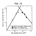
- Fig.19 shows a log-log graph showing a Nb concentration dependency of scattering time.
- the scattering (relaxation) time of the carrier rapidly increases with the increase of the Nb amount and gradually decreases from the point that the Nb substitutional amount x has achieved to 0.01. From the results of a ZnO thin film sample which is the same as a transparent conductor, it is considered that grain boundary scattering is dominant in x being less than 0.01 and scattering by neutral/ionized impurities is dominant in x being greater than 0.01 (see Fig. 19). As described above, regarding a sample having satisfactory carriers, since grain boundary scattering can be neglected even if the sample is a polycrystal sample, the polycrystal sample is able to maintain performance almost equal to that of the single crystal sample. This fact is a very advantageous point for developing an organic EL panel, a liquid crystal panel, or the like which necessarily use polycrystal thin films.
- the monotonical increase of the effective mass of carrier with the Nb amount suggests the decrease of curvature of the conductive band as the conductive band separates from the minimum of conduction band (variation is smaller than that of scattering time).
- the absolute value of variation is 0.2 to 0,4 m 0 (m 0 is the rest mass of an electron) and the value is almost equal to that of SnO 2 (0.2 to 0.3 m 0 ) or that of ITO (0.3 m 0 ).
- the tendency of mobility reflects the change of the Nb amount of scattering time in general. That is, the transport phenomenon at room temperature strongly depends on the change of a scattering mechanism with Nb addition rather than a band structure.
- the vicinity of x being 0.01 to 0.03 is the optimum composition in which both grain boundary scattering and impurity scattering can be suppressed to the minimum.
- metal oxide has the composition of Ti 1-x-y Nb x Ta y O 2 , the metal oxide can be sufficiently used until x+y becomes 0.3 by experimentation. As long as it is decided by X-ray measurement, it has been ascertained that x and y can be substituted to 40% (x+y is 0.4 or less). When it is desired that only blue-ultraviolet rays are transmitted even if transparency in the visible light region decreases, the metal oxide having a large substitutional ratio x+y is sufficiently used depending on use such as application to a heat reflecting film and thereby the maximum of x+y when Nb and Ta are mixed becomes larger.
- TiO 2 film may be provided by applying an oriented film being at least one selected from the group consisting of ZnO, ZrO 2 , SrTiO 3 , MgO, LaAlO 3 , CeO 2 , ZrO 2 , and Al 2 O 3 films on a substrate beforehand, and forming a TiO 2 film thereon.
- the oriented film acts as a buffer film (buffer layer),
- the buffer layer is important to form an anatase type film on glass. Since ZnO is easily oriented, there is an advantage that a ZnO film is easily formed.
- V, Mn, Tc, Re, P, Bi, and the like are applicable for using as a dopant which imparts transparent conductivity. All other elements have applicability for use as a dopant imparting transparent conductivity.
- transparent conductive materials are based on an oxide of Sn, In, or Zn, and oxide thin films such as ITO, SnO 2 , and ZnO are used as a transparent conductive film.
- Al or Ga is an effective dopant for a ZnO film.
- These elements are placed on the right side of the periodic table. It is known that these elements have an electric conduction mechanism based on an s electron or a p electron.
- electric conduction is imparted by a d electron, so the conductor is a new type of transparent conductor.
- the TiO 2 film may be grown on a GaN substrate.
- the present inventors have found that epitaxial growth of the TiO 2 film is performed on the GaN substrate. Concretely, the following composition is considered.
- Functional device characterized by comprising Al x Ga y In z N (0 ⁇ x ⁇ 1, 0 ⁇ y ⁇ 1, and 0 ⁇ z ⁇ 1) and an oxide material formed on the Al x Ga y In z N composed of a metal oxide which is TiO 2 .
- the metal oxide is doped with one or more elements selected from the group consisting of Nb, Ta, Mo, As, Sb, Al, and W.
- the metal oxide is doped with one or more elements selected from the group consisting of Co, Fe, Cr, Sn Ni, Mn, and V.
- the oxide material film may be formed by not only a PLD method, but also another physical vapor deposition (PVD) method such as a molecular beam epitaxy (MBE) method and a sputtering method, or a chemical vapor deposition (CVD) method, for example, a MOCVD method other than the PLD method.
- PVD physical vapor deposition
- MBE molecular beam epitaxy
- CVD chemical vapor deposition
- the oxide material can be used as an optical magnetic device showing a large Faraday rotation coefficient in the vicinity of a wavelength of 400 nm. Especially, since a large Faraday rotation coefficient equal to that of a magnetic garnet film is obtained, an optical isolator suitable for a next generation short wavelength region communication can be prepared using the oxide material.
- the oxide material can be used for a magneto-optical device such as an optical circulator, a variable optical attenuator, an optical communication device, or the like; a magneto-optical device: an optical circuit; a nonreciprocal optical part; a nonreciprocal optical element; a semiconductor laser equipped with an isolator; a current-magnetic field sensor; a magnetic domain observation; a magneto-optical measurement; or the like.
- optical isolator typical examples include a module comprising an LD and an isolator to be a unit; an optical isolator for fiber insertion; an optical isolator for an optical amplifier; a deflection-dependent type optical isolator, a deflection-independent type optical isolator; and an optical waveguide type optical isolator.
- optical waveguide optical isolator typical examples include a Mach-Zehnder type branching waveguide isolator and a rib type waveguide isolator.
- a deflection-dependent type circulator and a deflection-independent type circulator may be used.
- an optical isolator which also corresponds to a short wavelength region such as blue or ultraviolet is able to be achieved. If the optical isolator is formed on the TiO 2 film with epitaxial growth, a functional device is monolithically obtained as well as the TiO 2 film acts as a buffer for crystal growth. That is, development of a monolithic functional device as well as a highly efficient light emitting device and a display with a low-cost and a large area can be carried out. For example, the fusion of a transparent electrode and an optical device, and the fusion of a light emitting device and a magneto-optical device can be achieved.
- the oxide material may be used for a light receiving element, a high frequency device such as a HEMT (high electron mobility transistor) or the like, and an electronic device.
- an electrode for a dye sensitized solar cell a display panel, an organic EL panel, a light emitting element, a light emitting diode (LED), a transparent electrode of white LED or blue laser (film forming on the GaN), a transparent electrode for a vertical cavity surface emitting laser, a lighting device, a communication device, and an application that only blue light is made to transmit
- the transmittance is preferably 90% or greater in the visible light region and a long wavelength red light region may be filtered to pass only blue light.
- the thin layer doped with a large amount ofNb is effective in this case. It is not essential that transmittance becomes 90% or greater.
- the doping amount ofNb or the like is simply adjusted in accordance with the application or a balance between resistivity and transmittance.
- the GaN compound may include not only GaN but also GaN with a small amount of dopant.
- the transparent metal 1 examples include a transparent conductive film on a liquid crystal display (LCD), a transparent conductive film on a color filter part, a transparent conductive film on an electro luminescence (EL) display, a transparent conductive film on a plasma display panel (PDP), a PDP optical filter, a transparent conductive film for blocking electromagnetic waves, a transparent conductive film for blocking a near infrared ray, a transparent conductive film for preventing surface reflection, an optical filter, a touch panel, a resistive type touch panel, an electromagnetic induction type touch panel, an ultrasonic type touch panel, an optical touch panel, an electrical capacitance type touch panel, a resistive type touch panel for personal digital assistants, a touch panel unified with a display (inner touch panel), a solar cell, an amorphous (a-Si) solar cell, a microcrystalline Si thin film solar cell, a CIGS solar cell, a dye sensitized solar cell (
- a substrate for transparent electrode having transparency and conductivity is achieved and the substrate is able to be applied in various uses.
Landscapes
- Chemical & Material Sciences (AREA)
- Physics & Mathematics (AREA)
- Chemical Kinetics & Catalysis (AREA)
- General Chemical & Material Sciences (AREA)
- Nonlinear Science (AREA)
- Geochemistry & Mineralogy (AREA)
- Engineering & Computer Science (AREA)
- Organic Chemistry (AREA)
- Electrochemistry (AREA)
- Materials Engineering (AREA)
- Life Sciences & Earth Sciences (AREA)
- General Physics & Mathematics (AREA)
- Crystallography & Structural Chemistry (AREA)
- Mathematical Physics (AREA)
- Optics & Photonics (AREA)
- Inorganic Chemistry (AREA)
- Non-Insulated Conductors (AREA)
- Inorganic Compounds Of Heavy Metals (AREA)
- Liquid Crystal (AREA)
- Electroluminescent Light Sources (AREA)
- Physical Vapour Deposition (AREA)
- Devices For Indicating Variable Information By Combining Individual Elements (AREA)
- Conductive Materials (AREA)
Applications Claiming Priority (3)
| Application Number | Priority Date | Filing Date | Title |
|---|---|---|---|
| JP2004236125 | 2004-08-13 | ||
| JP2005044873 | 2005-02-21 | ||
| PCT/JP2005/014660 WO2006016608A1 (fr) | 2004-08-13 | 2005-08-10 | Conducteur transparent, électrode transparente, cellule solaire, dispositif luminescent et panneau d’affichage |
Publications (2)
| Publication Number | Publication Date |
|---|---|
| EP1796107A1 true EP1796107A1 (fr) | 2007-06-13 |
| EP1796107A4 EP1796107A4 (fr) | 2011-10-26 |
Family
ID=35839377
Family Applications (1)
| Application Number | Title | Priority Date | Filing Date |
|---|---|---|---|
| EP05770464A Withdrawn EP1796107A4 (fr) | 2004-08-13 | 2005-08-10 | Conducteur transparent, électrode transparente, cellule solaire, dispositif luminescent et panneau d"affichage |
Country Status (7)
| Country | Link |
|---|---|
| US (1) | US7858206B2 (fr) |
| EP (1) | EP1796107A4 (fr) |
| JP (1) | JP5132151B2 (fr) |
| KR (1) | KR20070048780A (fr) |
| CN (1) | CN101036200B (fr) |
| TW (1) | TWI382004B (fr) |
| WO (1) | WO2006016608A1 (fr) |
Cited By (6)
| Publication number | Priority date | Publication date | Assignee | Title |
|---|---|---|---|---|
| EP2128876A4 (fr) * | 2007-03-19 | 2010-03-03 | Asahi Glass Co Ltd | Procede de fabrication d'un conducteur electrique |
| WO2011139523A3 (fr) * | 2010-04-27 | 2012-02-02 | Ppg Industries Ohio, Inc. | Procédé de dépôt d'un film de dioxyde de titane dopé par du niobium sur un substrat et substrat revêtu fabriqué par ce procédé |
| WO2013016369A1 (fr) | 2011-07-28 | 2013-01-31 | Pilkington Group Limited | Apcvd d'oxyde de titane dopé et article revêtu obtenu par ce procédé |
| DE102012104374A1 (de) | 2012-05-21 | 2013-11-21 | Helmholtz-Zentrum Dresden - Rossendorf E.V. | Herstellung transparenter leitfähiger Titandioxidschichten, diese selbst und ihre Verwendung |
| EP2543507A4 (fr) * | 2010-03-02 | 2017-05-17 | Sumitomo Metal Mining Co., Ltd. | Stratifié, son procédé de production et élément fonctionnel l'utilisant |
| EP3770983A1 (fr) * | 2019-07-26 | 2021-01-27 | AIT Austrian Institute of Technology GmbH | Électrode conducteur transparent et son procédé de fabrication |
Families Citing this family (33)
| Publication number | Priority date | Publication date | Assignee | Title |
|---|---|---|---|---|
| US7968216B2 (en) * | 2005-01-08 | 2011-06-28 | Toyoda Gosei Co., Ltd. | Internal gear pump |
| JP2007073198A (ja) * | 2005-09-02 | 2007-03-22 | Toyota Central Res & Dev Lab Inc | 色素増感型太陽電池 |
| JP4926504B2 (ja) * | 2006-03-08 | 2012-05-09 | 浜松ホトニクス株式会社 | 光電面、それを備える電子管及び光電面の製造方法 |
| JP2008084824A (ja) * | 2006-03-20 | 2008-04-10 | Kanagawa Acad Of Sci & Technol | 導電体の製造方法 |
| JP2008029125A (ja) * | 2006-07-21 | 2008-02-07 | Sony Corp | 電磁誘導型処理装置 |
| US20080047603A1 (en) * | 2006-08-24 | 2008-02-28 | Guardian Industries Corp. | Front contact with intermediate layer(s) adjacent thereto for use in photovoltaic device and method of making same |
| TWI550646B (zh) * | 2006-10-12 | 2016-09-21 | 坎畢歐科技公司 | 製造透明導體之方法 |
| WO2008044474A1 (fr) * | 2006-10-12 | 2008-04-17 | Konica Minolta Holdings, Inc. | Procédé de formation de film transparent électroconducteur |
| JP5326383B2 (ja) * | 2007-07-10 | 2013-10-30 | 豊田合成株式会社 | 発光装置 |
| CN101785071A (zh) * | 2007-08-29 | 2010-07-21 | 旭硝子株式会社 | 导电体层的制造方法 |
| JP5308117B2 (ja) * | 2007-10-29 | 2013-10-09 | 住友化学株式会社 | 透明導電性基板の製造方法 |
| US7888594B2 (en) * | 2007-11-20 | 2011-02-15 | Guardian Industries Corp. | Photovoltaic device including front electrode having titanium oxide inclusive layer with high refractive index |
| JP5173512B2 (ja) * | 2008-03-25 | 2013-04-03 | 財団法人神奈川科学技術アカデミー | 導電体およびその製造方法 |
| JP5624712B2 (ja) * | 2008-09-01 | 2014-11-12 | 豊田合成株式会社 | TiO2からなる導電性透明層の製造方法及び当該導電性透明層の製造方法を利用した半導体発光素子の製造方法 |
| WO2010063530A2 (fr) * | 2008-11-05 | 2010-06-10 | Oerlikon Solar Ip Ag, Truebbach | Dispositif de cellules solaires et procédé de fabrication associé |
| JP2010231172A (ja) * | 2009-03-04 | 2010-10-14 | Seiko Epson Corp | 光学物品およびその製造方法 |
| WO2010135576A2 (fr) | 2009-05-21 | 2010-11-25 | Cornell Research Foundation, Inc. | Nanoparticules d'oxyde métallique et de nitrure métallique conductrices |
| US20100310856A1 (en) * | 2009-06-04 | 2010-12-09 | Freiman Stephen W | Transparent materials having enhanced resistance to crack growth |
| JP5588135B2 (ja) | 2009-08-10 | 2014-09-10 | ホーヤ レンズ マニュファクチャリング フィリピン インク | 光学物品の製造方法 |
| JP2011060447A (ja) * | 2009-09-07 | 2011-03-24 | Kanagawa Acad Of Sci & Technol | 導電体基板、導電体基板の製造方法、デバイス及び電子機器 |
| JP5561358B2 (ja) | 2010-03-19 | 2014-07-30 | 住友金属鉱山株式会社 | 透明導電膜 |
| CN101950605B (zh) * | 2010-07-23 | 2012-03-21 | 四川大学 | 柔性基体材料表面获取多孔高纯锐钛矿相二氧化钛薄膜的工艺 |
| JP2012032690A (ja) | 2010-08-02 | 2012-02-16 | Seiko Epson Corp | 光学物品およびその製造方法 |
| CN102453868A (zh) * | 2010-10-27 | 2012-05-16 | 鸿富锦精密工业(深圳)有限公司 | 镀膜件及其制备方法 |
| TWI491753B (zh) * | 2010-10-29 | 2015-07-11 | 鴻海精密工業股份有限公司 | 鍍膜件及其製備方法 |
| JP5943318B2 (ja) * | 2011-07-29 | 2016-07-05 | 国立大学法人島根大学 | 透明導電膜作成方法 |
| CN104124375A (zh) * | 2013-04-24 | 2014-10-29 | 海洋王照明科技股份有限公司 | 一种有机电致发光器件及其制备方法 |
| KR102309880B1 (ko) | 2014-12-08 | 2021-10-06 | 삼성전자주식회사 | 전도성 박막 |
| KR101856726B1 (ko) * | 2014-12-08 | 2018-05-10 | 주식회사 엘지화학 | 유무기 하이브리드 페로브스카이트 화합물, 이의 제조방법 및 이를 포함하는 태양전지 |
| JP6931538B2 (ja) * | 2017-02-23 | 2021-09-08 | アルバック成膜株式会社 | マスクブランクス及びフォトマスク |
| GB201820427D0 (en) * | 2018-12-14 | 2019-01-30 | Univ Oxford Innovation Ltd | Device interlayer |
| CN112853266B (zh) * | 2021-01-05 | 2023-02-28 | 西京学院 | 一种柔性透明太阳能水解光电极及其制备方法 |
| CN113235048A (zh) * | 2021-04-30 | 2021-08-10 | 中国建筑材料科学研究总院有限公司 | 纳米晶二氧化钛功能薄膜及其制备方法 |
Family Cites Families (19)
| Publication number | Priority date | Publication date | Assignee | Title |
|---|---|---|---|---|
| JPH02191330A (ja) * | 1988-09-29 | 1990-07-27 | Taiyo Yuden Co Ltd | 酸化チタン薄膜及びその製法 |
| US5419824A (en) * | 1992-11-12 | 1995-05-30 | Weres; Oleh | Electrode, electrode manufacturing process and electrochemical cell |
| US6387844B1 (en) * | 1994-10-31 | 2002-05-14 | Akira Fujishima | Titanium dioxide photocatalyst |
| CN1158429A (zh) * | 1996-12-19 | 1997-09-03 | 浙江大学 | 大屏幕投影用电选址反射型液晶光阀 |
| JP3019797B2 (ja) * | 1997-02-07 | 2000-03-13 | 日本電気株式会社 | 固体撮像素子とその製造方法 |
| JP2000208800A (ja) * | 1998-11-13 | 2000-07-28 | Fuji Xerox Co Ltd | 太陽電池及びそれを用いた自己電力供給型表示素子、並びに太陽電池の製造方法 |
| JP2000260355A (ja) * | 1999-03-05 | 2000-09-22 | Ricoh Co Ltd | ディスプレイ |
| JP3824889B2 (ja) * | 2000-07-14 | 2006-09-20 | セイコーエプソン株式会社 | カラーフィルタ基板及び液晶装置、並びにこれらの製造方法 |
| EP1207572A1 (fr) * | 2000-11-15 | 2002-05-22 | Dr. Sugnaux Consulting | Electrodes mésoporeuses pour cellules électrochimiques et leur méthode de production |
| JP2002212463A (ja) * | 2001-01-12 | 2002-07-31 | Sustainable Titania Technology Inc | チタン酸化物含有導電性被膜形成液、該形成液製造方法及びチタン酸化物含有膜を備える構造体 |
| US7202412B2 (en) * | 2002-01-18 | 2007-04-10 | Sharp Kabushiki Kaisha | Photovoltaic cell including porous semiconductor layer, method of manufacturing the same and solar cell |
| US6950220B2 (en) * | 2002-03-18 | 2005-09-27 | E Ink Corporation | Electro-optic displays, and methods for driving same |
| JP3692472B2 (ja) * | 2002-03-25 | 2005-09-07 | テイカ株式会社 | 導電性酸化チタンポーラス厚膜の低温合成 |
| JP2004095240A (ja) | 2002-08-30 | 2004-03-25 | Mitsui Chemicals Inc | 透明電極 |
| JP4242132B2 (ja) * | 2002-09-25 | 2009-03-18 | 株式会社クリスタルシステム | 透明帯電防止板およびその製造方法 |
| US6885065B2 (en) * | 2002-11-20 | 2005-04-26 | Freescale Semiconductor, Inc. | Ferromagnetic semiconductor structure and method for forming the same |
| JP2004311783A (ja) * | 2003-04-08 | 2004-11-04 | Fuji Xerox Co Ltd | 光検出装置、及びその実装方法 |
| JP4362322B2 (ja) * | 2003-06-20 | 2009-11-11 | 日本板硝子株式会社 | 透明導電性基板およびその製造方法ならびに光電変換素子 |
| JP2005072367A (ja) * | 2003-08-26 | 2005-03-17 | Nippon Oil Corp | 光電変換素子 |
-
2005
- 2005-08-10 WO PCT/JP2005/014660 patent/WO2006016608A1/fr not_active Ceased
- 2005-08-10 US US11/573,678 patent/US7858206B2/en not_active Expired - Fee Related
- 2005-08-10 JP JP2006531685A patent/JP5132151B2/ja not_active Expired - Fee Related
- 2005-08-10 KR KR1020077005595A patent/KR20070048780A/ko not_active Ceased
- 2005-08-10 CN CN2005800338375A patent/CN101036200B/zh not_active Expired - Fee Related
- 2005-08-10 EP EP05770464A patent/EP1796107A4/fr not_active Withdrawn
- 2005-08-12 TW TW094127601A patent/TWI382004B/zh not_active IP Right Cessation
Cited By (8)
| Publication number | Priority date | Publication date | Assignee | Title |
|---|---|---|---|---|
| EP2128876A4 (fr) * | 2007-03-19 | 2010-03-03 | Asahi Glass Co Ltd | Procede de fabrication d'un conducteur electrique |
| EP2543507A4 (fr) * | 2010-03-02 | 2017-05-17 | Sumitomo Metal Mining Co., Ltd. | Stratifié, son procédé de production et élément fonctionnel l'utilisant |
| WO2011139523A3 (fr) * | 2010-04-27 | 2012-02-02 | Ppg Industries Ohio, Inc. | Procédé de dépôt d'un film de dioxyde de titane dopé par du niobium sur un substrat et substrat revêtu fabriqué par ce procédé |
| US8551609B2 (en) | 2010-04-27 | 2013-10-08 | Ppg Industries Ohio, Inc. | Method of depositing niobium doped titania film on a substrate and the coated substrate made thereby |
| WO2013016369A1 (fr) | 2011-07-28 | 2013-01-31 | Pilkington Group Limited | Apcvd d'oxyde de titane dopé et article revêtu obtenu par ce procédé |
| DE102012104374A1 (de) | 2012-05-21 | 2013-11-21 | Helmholtz-Zentrum Dresden - Rossendorf E.V. | Herstellung transparenter leitfähiger Titandioxidschichten, diese selbst und ihre Verwendung |
| WO2013174824A1 (fr) | 2012-05-21 | 2013-11-28 | Helmholtz-Zentrum Dresden - Rossendorf E.V. | Production de couches de dioxyde de titane conductrices transparentes, couches ainsi produites et leur utilisation |
| EP3770983A1 (fr) * | 2019-07-26 | 2021-01-27 | AIT Austrian Institute of Technology GmbH | Électrode conducteur transparent et son procédé de fabrication |
Also Published As
| Publication number | Publication date |
|---|---|
| TWI382004B (zh) | 2013-01-11 |
| KR20070048780A (ko) | 2007-05-09 |
| TW200606122A (en) | 2006-02-16 |
| EP1796107A4 (fr) | 2011-10-26 |
| WO2006016608A1 (fr) | 2006-02-16 |
| JPWO2006016608A1 (ja) | 2008-05-01 |
| CN101036200B (zh) | 2010-12-29 |
| US20070287025A1 (en) | 2007-12-13 |
| CN101036200A (zh) | 2007-09-12 |
| US7858206B2 (en) | 2010-12-28 |
| JP5132151B2 (ja) | 2013-01-30 |
Similar Documents
| Publication | Publication Date | Title |
|---|---|---|
| US7858206B2 (en) | Transparent conductor, transparent electrode, solar cell, light emitting device and display panel | |
| JP4170454B2 (ja) | 透明導電性酸化物薄膜を有する物品及びその製造方法 | |
| TWI400721B (zh) | The manufacturing method of the conductor | |
| JP7091577B2 (ja) | 金属酸化物薄膜、金属酸化物薄膜を堆積する方法及び金属酸化物薄膜を備える装置 | |
| JP5296691B2 (ja) | 導電体層の製造方法 | |
| Jayathilake et al. | Overview on transparent conducting oxides and state of the art of low-cost doped ZnO systems | |
| JP2008084824A (ja) | 導電体の製造方法 | |
| Ghanem et al. | Synthesis and characterization of undoped and Er-doped ZnO nano-structure thin films deposited by sol-gel spin coating technique | |
| JP3945887B2 (ja) | 導電性酸化物薄膜を有する物品及びその製造方法 | |
| Meher et al. | Effect of post-annealing on the band gap of sol–gel prepared nano-crystalline Mg x Zn1− x O (0.0≤ x≤ 0.3) thin films | |
| EP0707320A1 (fr) | Conducteurs transparents comprenant de l'oxyde de zinc et d'indium et méthodes de fabrication de films | |
| JP2010231972A (ja) | 導電体基板、導電体基板の製造方法、デバイス及び電子機器 | |
| CN100530552C (zh) | 功能元件和氧化物材料形成方法 | |
| Xiao et al. | Impact of In-doping and post-annealing on the properties of SnO2 thin films deposited by magnetron sputtering | |
| Lung et al. | Characterization of the aluminum concentration upon the properties of aluminum zinc oxide thin films | |
| JP2008050677A (ja) | 金属酸化物膜 | |
| JP2001133814A (ja) | 自己電力供給型調光素子 | |
| Zhao et al. | Optical Properties of Mg x Zn1− x O Polycrystalline Thin Films Prepared by Sol-Gel Deposition Method | |
| Ishizawa et al. | A significant increase in carrier concentration in TiO2 by Sm doping | |
| US7968216B2 (en) | Internal gear pump | |
| Otieno et al. | Structural and Optical Probe into Rare Earth Doped ZnO for Spectral Conversion in Solar Cells | |
| JP2011060447A (ja) | 導電体基板、導電体基板の製造方法、デバイス及び電子機器 | |
| Issam et al. | Effect of Strontium (Sr) Doping on the Structural, Electronic and Optical Properties of Zno, by First-Principles Calculations | |
| Yuan et al. | ZnO thin films prepared by ion beam enhanced deposition method |
Legal Events
| Date | Code | Title | Description |
|---|---|---|---|
| PUAI | Public reference made under article 153(3) epc to a published international application that has entered the european phase |
Free format text: ORIGINAL CODE: 0009012 |
|
| 17P | Request for examination filed |
Effective date: 20070309 |
|
| AK | Designated contracting states |
Kind code of ref document: A1 Designated state(s): AT BE BG CH CY CZ DE DK EE ES FI FR GB GR HU IE IS IT LI LT LU LV MC NL PL PT RO SE SI SK TR |
|
| RIN1 | Information on inventor provided before grant (corrected) |
Inventor name: HASEGAWA, TETSUYA 3-11-3-502 KUSUNOKIDAI Inventor name: FURUBAYASHI, YUTAKA Inventor name: HITOSUGI, TARO |
|
| DAX | Request for extension of the european patent (deleted) | ||
| A4 | Supplementary search report drawn up and despatched |
Effective date: 20110927 |
|
| RIC1 | Information provided on ipc code assigned before grant |
Ipc: H05B 33/28 20060101ALI20110921BHEP Ipc: H01M 14/00 20060101ALI20110921BHEP Ipc: G09F 9/30 20060101ALI20110921BHEP Ipc: G02F 1/1343 20060101ALI20110921BHEP Ipc: H01B 5/14 20060101AFI20110921BHEP Ipc: H05B 33/14 20060101ALI20110921BHEP |
|
| 17Q | First examination report despatched |
Effective date: 20121106 |
|
| GRAP | Despatch of communication of intention to grant a patent |
Free format text: ORIGINAL CODE: EPIDOSNIGR1 |
|
| INTG | Intention to grant announced |
Effective date: 20160930 |
|
| RIC1 | Information provided on ipc code assigned before grant |
Ipc: H05B 33/14 20060101ALI20160920BHEP Ipc: G02F 1/1343 20060101ALI20160920BHEP Ipc: H01M 14/00 20060101ALI20160920BHEP Ipc: H01L 31/18 20060101ALI20160920BHEP Ipc: H05B 33/28 20060101ALI20160920BHEP Ipc: H01B 5/14 20060101AFI20160920BHEP Ipc: H01B 1/08 20060101ALI20160920BHEP Ipc: C03C 17/245 20060101ALI20160920BHEP Ipc: H01L 31/0224 20060101ALI20160920BHEP Ipc: H01M 4/48 20060101ALI20160920BHEP Ipc: G09F 9/30 20060101ALI20160920BHEP Ipc: C03C 17/34 20060101ALI20160920BHEP |
|
| STAA | Information on the status of an ep patent application or granted ep patent |
Free format text: STATUS: THE APPLICATION IS DEEMED TO BE WITHDRAWN |
|
| 18D | Application deemed to be withdrawn |
Effective date: 20170211 |