EP1796156B1 - Flip-chip-anbringverfahren - Google Patents
Flip-chip-anbringverfahren Download PDFInfo
- Publication number
- EP1796156B1 EP1796156B1 EP05782249.6A EP05782249A EP1796156B1 EP 1796156 B1 EP1796156 B1 EP 1796156B1 EP 05782249 A EP05782249 A EP 05782249A EP 1796156 B1 EP1796156 B1 EP 1796156B1
- Authority
- EP
- European Patent Office
- Prior art keywords
- resin
- wiring substrate
- solder powder
- semiconductor chip
- flip chip
- Prior art date
- Legal status (The legal status is an assumption and is not a legal conclusion. Google has not performed a legal analysis and makes no representation as to the accuracy of the status listed.)
- Expired - Lifetime
Links
Images


Classifications
-
- H—ELECTRICITY
- H10—SEMICONDUCTOR DEVICES; ELECTRIC SOLID-STATE DEVICES NOT OTHERWISE PROVIDED FOR
- H10W—GENERIC PACKAGES, INTERCONNECTIONS, CONNECTORS OR OTHER CONSTRUCTIONAL DETAILS OF DEVICES COVERED BY CLASS H10
- H10W74/00—Encapsulations, e.g. protective coatings
- H10W74/01—Manufacture or treatment
- H10W74/012—Manufacture or treatment of encapsulations on active surfaces of flip-chip devices, e.g. forming underfills
-
- H—ELECTRICITY
- H05—ELECTRIC TECHNIQUES NOT OTHERWISE PROVIDED FOR
- H05K—PRINTED CIRCUITS; CASINGS OR CONSTRUCTIONAL DETAILS OF ELECTRIC APPARATUS; MANUFACTURE OF ASSEMBLAGES OF ELECTRICAL COMPONENTS
- H05K3/00—Apparatus or processes for manufacturing printed circuits
- H05K3/30—Assembling printed circuits with electric components, e.g. with resistors
- H05K3/32—Assembling printed circuits with electric components, e.g. with resistors electrically connecting electric components or wires to printed circuits
- H05K3/34—Assembling printed circuits with electric components, e.g. with resistors electrically connecting electric components or wires to printed circuits by soldering
- H05K3/3465—Application of solder
- H05K3/3485—Application of solder paste, slurry or powder
-
- H—ELECTRICITY
- H10—SEMICONDUCTOR DEVICES; ELECTRIC SOLID-STATE DEVICES NOT OTHERWISE PROVIDED FOR
- H10P—GENERIC PROCESSES OR APPARATUS FOR THE MANUFACTURE OR TREATMENT OF DEVICES COVERED BY CLASS H10
- H10P72/00—Handling or holding of wafers, substrates or devices during manufacture or treatment thereof
- H10P72/70—Handling or holding of wafers, substrates or devices during manufacture or treatment thereof for supporting or gripping
- H10P72/74—Handling or holding of wafers, substrates or devices during manufacture or treatment thereof for supporting or gripping using temporarily an auxiliary support
-
- H—ELECTRICITY
- H10—SEMICONDUCTOR DEVICES; ELECTRIC SOLID-STATE DEVICES NOT OTHERWISE PROVIDED FOR
- H10W—GENERIC PACKAGES, INTERCONNECTIONS, CONNECTORS OR OTHER CONSTRUCTIONAL DETAILS OF DEVICES COVERED BY CLASS H10
- H10W74/00—Encapsulations, e.g. protective coatings
- H10W74/10—Encapsulations, e.g. protective coatings characterised by their shape or disposition
- H10W74/15—Encapsulations, e.g. protective coatings characterised by their shape or disposition on active surfaces of flip-chip devices, e.g. underfills
-
- H—ELECTRICITY
- H05—ELECTRIC TECHNIQUES NOT OTHERWISE PROVIDED FOR
- H05K—PRINTED CIRCUITS; CASINGS OR CONSTRUCTIONAL DETAILS OF ELECTRIC APPARATUS; MANUFACTURE OF ASSEMBLAGES OF ELECTRICAL COMPONENTS
- H05K2201/00—Indexing scheme relating to printed circuits covered by H05K1/00
- H05K2201/10—Details of components or other objects attached to or integrated in a printed circuit board
- H05K2201/10613—Details of electrical connections of non-printed components, e.g. special leads
- H05K2201/10954—Other details of electrical connections
- H05K2201/10977—Encapsulated connections
-
- H—ELECTRICITY
- H05—ELECTRIC TECHNIQUES NOT OTHERWISE PROVIDED FOR
- H05K—PRINTED CIRCUITS; CASINGS OR CONSTRUCTIONAL DETAILS OF ELECTRIC APPARATUS; MANUFACTURE OF ASSEMBLAGES OF ELECTRICAL COMPONENTS
- H05K2203/00—Indexing scheme relating to apparatus or processes for manufacturing printed circuits covered by H05K3/00
- H05K2203/02—Details related to mechanical or acoustic processing, e.g. drilling, punching, cutting, using ultrasound
- H05K2203/0278—Flat pressure, e.g. for connecting terminals with anisotropic conductive adhesive
-
- H—ELECTRICITY
- H05—ELECTRIC TECHNIQUES NOT OTHERWISE PROVIDED FOR
- H05K—PRINTED CIRCUITS; CASINGS OR CONSTRUCTIONAL DETAILS OF ELECTRIC APPARATUS; MANUFACTURE OF ASSEMBLAGES OF ELECTRICAL COMPONENTS
- H05K2203/00—Indexing scheme relating to apparatus or processes for manufacturing printed circuits covered by H05K3/00
- H05K2203/04—Soldering or other types of metallurgic bonding
- H05K2203/0425—Solder powder or solder coated metal powder
-
- H—ELECTRICITY
- H05—ELECTRIC TECHNIQUES NOT OTHERWISE PROVIDED FOR
- H05K—PRINTED CIRCUITS; CASINGS OR CONSTRUCTIONAL DETAILS OF ELECTRIC APPARATUS; MANUFACTURE OF ASSEMBLAGES OF ELECTRICAL COMPONENTS
- H05K3/00—Apparatus or processes for manufacturing printed circuits
- H05K3/30—Assembling printed circuits with electric components, e.g. with resistors
- H05K3/32—Assembling printed circuits with electric components, e.g. with resistors electrically connecting electric components or wires to printed circuits
- H05K3/321—Assembling printed circuits with electric components, e.g. with resistors electrically connecting electric components or wires to printed circuits by conductive adhesives
- H05K3/323—Assembling printed circuits with electric components, e.g. with resistors electrically connecting electric components or wires to printed circuits by conductive adhesives by applying an anisotropic conductive adhesive layer over an array of pads
-
- H—ELECTRICITY
- H05—ELECTRIC TECHNIQUES NOT OTHERWISE PROVIDED FOR
- H05K—PRINTED CIRCUITS; CASINGS OR CONSTRUCTIONAL DETAILS OF ELECTRIC APPARATUS; MANUFACTURE OF ASSEMBLAGES OF ELECTRICAL COMPONENTS
- H05K3/00—Apparatus or processes for manufacturing printed circuits
- H05K3/30—Assembling printed circuits with electric components, e.g. with resistors
- H05K3/32—Assembling printed circuits with electric components, e.g. with resistors electrically connecting electric components or wires to printed circuits
- H05K3/34—Assembling printed circuits with electric components, e.g. with resistors electrically connecting electric components or wires to printed circuits by soldering
- H05K3/341—Surface mounted components
- H05K3/3431—Leadless components
- H05K3/3436—Leadless components having an array of bottom contacts, e.g. pad grid array or ball grid array components
-
- H—ELECTRICITY
- H10—SEMICONDUCTOR DEVICES; ELECTRIC SOLID-STATE DEVICES NOT OTHERWISE PROVIDED FOR
- H10W—GENERIC PACKAGES, INTERCONNECTIONS, CONNECTORS OR OTHER CONSTRUCTIONAL DETAILS OF DEVICES COVERED BY CLASS H10
- H10W72/00—Interconnections or connectors in packages
- H10W72/01—Manufacture or treatment
- H10W72/012—Manufacture or treatment of bump connectors, dummy bumps or thermal bumps
- H10W72/01204—Manufacture or treatment of bump connectors, dummy bumps or thermal bumps using temporary auxiliary members, e.g. using sacrificial coatings or handle substrates
-
- H—ELECTRICITY
- H10—SEMICONDUCTOR DEVICES; ELECTRIC SOLID-STATE DEVICES NOT OTHERWISE PROVIDED FOR
- H10W—GENERIC PACKAGES, INTERCONNECTIONS, CONNECTORS OR OTHER CONSTRUCTIONAL DETAILS OF DEVICES COVERED BY CLASS H10
- H10W72/00—Interconnections or connectors in packages
- H10W72/01—Manufacture or treatment
- H10W72/012—Manufacture or treatment of bump connectors, dummy bumps or thermal bumps
- H10W72/01261—Chemical or physical modification, e.g. by sintering or anodisation
-
- H—ELECTRICITY
- H10—SEMICONDUCTOR DEVICES; ELECTRIC SOLID-STATE DEVICES NOT OTHERWISE PROVIDED FOR
- H10W—GENERIC PACKAGES, INTERCONNECTIONS, CONNECTORS OR OTHER CONSTRUCTIONAL DETAILS OF DEVICES COVERED BY CLASS H10
- H10W72/00—Interconnections or connectors in packages
- H10W72/071—Connecting or disconnecting
- H10W72/072—Connecting or disconnecting of bump connectors
- H10W72/07231—Techniques
-
- H—ELECTRICITY
- H10—SEMICONDUCTOR DEVICES; ELECTRIC SOLID-STATE DEVICES NOT OTHERWISE PROVIDED FOR
- H10W—GENERIC PACKAGES, INTERCONNECTIONS, CONNECTORS OR OTHER CONSTRUCTIONAL DETAILS OF DEVICES COVERED BY CLASS H10
- H10W72/00—Interconnections or connectors in packages
- H10W72/071—Connecting or disconnecting
- H10W72/072—Connecting or disconnecting of bump connectors
- H10W72/07251—Connecting or disconnecting of bump connectors characterised by changes in properties of the bump connectors during connecting
- H10W72/07252—Connecting or disconnecting of bump connectors characterised by changes in properties of the bump connectors during connecting changes in structures or sizes
-
- H—ELECTRICITY
- H10—SEMICONDUCTOR DEVICES; ELECTRIC SOLID-STATE DEVICES NOT OTHERWISE PROVIDED FOR
- H10W—GENERIC PACKAGES, INTERCONNECTIONS, CONNECTORS OR OTHER CONSTRUCTIONAL DETAILS OF DEVICES COVERED BY CLASS H10
- H10W72/00—Interconnections or connectors in packages
- H10W72/071—Connecting or disconnecting
- H10W72/073—Connecting or disconnecting of die-attach connectors
- H10W72/07331—Connecting techniques
- H10W72/07332—Compression bonding, e.g. thermocompression bonding
-
- H—ELECTRICITY
- H10—SEMICONDUCTOR DEVICES; ELECTRIC SOLID-STATE DEVICES NOT OTHERWISE PROVIDED FOR
- H10W—GENERIC PACKAGES, INTERCONNECTIONS, CONNECTORS OR OTHER CONSTRUCTIONAL DETAILS OF DEVICES COVERED BY CLASS H10
- H10W72/00—Interconnections or connectors in packages
- H10W72/071—Connecting or disconnecting
- H10W72/073—Connecting or disconnecting of die-attach connectors
- H10W72/07351—Connecting or disconnecting of die-attach connectors characterised by changes in properties of the die-attach connectors during connecting
- H10W72/07353—Connecting or disconnecting of die-attach connectors characterised by changes in properties of the die-attach connectors during connecting changes in shapes
-
- H—ELECTRICITY
- H10—SEMICONDUCTOR DEVICES; ELECTRIC SOLID-STATE DEVICES NOT OTHERWISE PROVIDED FOR
- H10W—GENERIC PACKAGES, INTERCONNECTIONS, CONNECTORS OR OTHER CONSTRUCTIONAL DETAILS OF DEVICES COVERED BY CLASS H10
- H10W72/00—Interconnections or connectors in packages
- H10W72/20—Bump connectors, e.g. solder bumps or copper pillars; Dummy bumps; Thermal bumps
- H10W72/221—Structures or relative sizes
- H10W72/225—Bumps having a filler embedded in a matrix
-
- H—ELECTRICITY
- H10—SEMICONDUCTOR DEVICES; ELECTRIC SOLID-STATE DEVICES NOT OTHERWISE PROVIDED FOR
- H10W—GENERIC PACKAGES, INTERCONNECTIONS, CONNECTORS OR OTHER CONSTRUCTIONAL DETAILS OF DEVICES COVERED BY CLASS H10
- H10W72/00—Interconnections or connectors in packages
- H10W72/20—Bump connectors, e.g. solder bumps or copper pillars; Dummy bumps; Thermal bumps
- H10W72/241—Dispositions, e.g. layouts
-
- H—ELECTRICITY
- H10—SEMICONDUCTOR DEVICES; ELECTRIC SOLID-STATE DEVICES NOT OTHERWISE PROVIDED FOR
- H10W—GENERIC PACKAGES, INTERCONNECTIONS, CONNECTORS OR OTHER CONSTRUCTIONAL DETAILS OF DEVICES COVERED BY CLASS H10
- H10W72/00—Interconnections or connectors in packages
- H10W72/20—Bump connectors, e.g. solder bumps or copper pillars; Dummy bumps; Thermal bumps
- H10W72/251—Materials
- H10W72/252—Materials comprising solid metals or solid metalloids, e.g. PbSn, Ag or Cu
-
- H—ELECTRICITY
- H10—SEMICONDUCTOR DEVICES; ELECTRIC SOLID-STATE DEVICES NOT OTHERWISE PROVIDED FOR
- H10W—GENERIC PACKAGES, INTERCONNECTIONS, CONNECTORS OR OTHER CONSTRUCTIONAL DETAILS OF DEVICES COVERED BY CLASS H10
- H10W72/00—Interconnections or connectors in packages
- H10W72/20—Bump connectors, e.g. solder bumps or copper pillars; Dummy bumps; Thermal bumps
- H10W72/251—Materials
- H10W72/253—Materials not comprising solid metals or solid metalloids, e.g. polymers or ceramics
-
- H—ELECTRICITY
- H10—SEMICONDUCTOR DEVICES; ELECTRIC SOLID-STATE DEVICES NOT OTHERWISE PROVIDED FOR
- H10W—GENERIC PACKAGES, INTERCONNECTIONS, CONNECTORS OR OTHER CONSTRUCTIONAL DETAILS OF DEVICES COVERED BY CLASS H10
- H10W72/00—Interconnections or connectors in packages
- H10W72/30—Die-attach connectors
- H10W72/321—Structures or relative sizes of die-attach connectors
- H10W72/325—Die-attach connectors having a filler embedded in a matrix
-
- H—ELECTRICITY
- H10—SEMICONDUCTOR DEVICES; ELECTRIC SOLID-STATE DEVICES NOT OTHERWISE PROVIDED FOR
- H10W—GENERIC PACKAGES, INTERCONNECTIONS, CONNECTORS OR OTHER CONSTRUCTIONAL DETAILS OF DEVICES COVERED BY CLASS H10
- H10W72/00—Interconnections or connectors in packages
- H10W72/30—Die-attach connectors
- H10W72/331—Shapes of die-attach connectors
- H10W72/332—Plan-view shape, i.e. in top view
-
- H—ELECTRICITY
- H10—SEMICONDUCTOR DEVICES; ELECTRIC SOLID-STATE DEVICES NOT OTHERWISE PROVIDED FOR
- H10W—GENERIC PACKAGES, INTERCONNECTIONS, CONNECTORS OR OTHER CONSTRUCTIONAL DETAILS OF DEVICES COVERED BY CLASS H10
- H10W72/00—Interconnections or connectors in packages
- H10W72/30—Die-attach connectors
- H10W72/341—Dispositions of die-attach connectors, e.g. layouts
- H10W72/344—Dispositions of die-attach connectors, e.g. layouts relative to underlying supporting features, e.g. bond pads, RDLs or vias
-
- H—ELECTRICITY
- H10—SEMICONDUCTOR DEVICES; ELECTRIC SOLID-STATE DEVICES NOT OTHERWISE PROVIDED FOR
- H10W—GENERIC PACKAGES, INTERCONNECTIONS, CONNECTORS OR OTHER CONSTRUCTIONAL DETAILS OF DEVICES COVERED BY CLASS H10
- H10W72/00—Interconnections or connectors in packages
- H10W72/30—Die-attach connectors
- H10W72/351—Materials of die-attach connectors
- H10W72/352—Materials of die-attach connectors comprising metals or metalloids, e.g. solders
-
- H—ELECTRICITY
- H10—SEMICONDUCTOR DEVICES; ELECTRIC SOLID-STATE DEVICES NOT OTHERWISE PROVIDED FOR
- H10W—GENERIC PACKAGES, INTERCONNECTIONS, CONNECTORS OR OTHER CONSTRUCTIONAL DETAILS OF DEVICES COVERED BY CLASS H10
- H10W72/00—Interconnections or connectors in packages
- H10W72/30—Die-attach connectors
- H10W72/351—Materials of die-attach connectors
- H10W72/353—Materials of die-attach connectors not comprising solid metals or solid metalloids, e.g. ceramics
- H10W72/354—Materials of die-attach connectors not comprising solid metals or solid metalloids, e.g. ceramics comprising polymers
-
- H—ELECTRICITY
- H10—SEMICONDUCTOR DEVICES; ELECTRIC SOLID-STATE DEVICES NOT OTHERWISE PROVIDED FOR
- H10W—GENERIC PACKAGES, INTERCONNECTIONS, CONNECTORS OR OTHER CONSTRUCTIONAL DETAILS OF DEVICES COVERED BY CLASS H10
- H10W72/00—Interconnections or connectors in packages
- H10W72/851—Dispositions of multiple connectors or interconnections
- H10W72/853—On the same surface
- H10W72/856—Bump connectors and die-attach connectors
-
- H—ELECTRICITY
- H10—SEMICONDUCTOR DEVICES; ELECTRIC SOLID-STATE DEVICES NOT OTHERWISE PROVIDED FOR
- H10W—GENERIC PACKAGES, INTERCONNECTIONS, CONNECTORS OR OTHER CONSTRUCTIONAL DETAILS OF DEVICES COVERED BY CLASS H10
- H10W72/00—Interconnections or connectors in packages
- H10W72/90—Bond pads, in general
- H10W72/941—Dispositions of bond pads
- H10W72/9415—Dispositions of bond pads relative to the surface, e.g. recessed, protruding
-
- H—ELECTRICITY
- H10—SEMICONDUCTOR DEVICES; ELECTRIC SOLID-STATE DEVICES NOT OTHERWISE PROVIDED FOR
- H10W—GENERIC PACKAGES, INTERCONNECTIONS, CONNECTORS OR OTHER CONSTRUCTIONAL DETAILS OF DEVICES COVERED BY CLASS H10
- H10W72/00—Interconnections or connectors in packages
- H10W72/90—Bond pads, in general
- H10W72/941—Dispositions of bond pads
- H10W72/944—Dispositions of multiple bond pads
- H10W72/9445—Top-view layouts, e.g. mirror arrays
-
- H—ELECTRICITY
- H10—SEMICONDUCTOR DEVICES; ELECTRIC SOLID-STATE DEVICES NOT OTHERWISE PROVIDED FOR
- H10W—GENERIC PACKAGES, INTERCONNECTIONS, CONNECTORS OR OTHER CONSTRUCTIONAL DETAILS OF DEVICES COVERED BY CLASS H10
- H10W74/00—Encapsulations, e.g. protective coatings
-
- H—ELECTRICITY
- H10—SEMICONDUCTOR DEVICES; ELECTRIC SOLID-STATE DEVICES NOT OTHERWISE PROVIDED FOR
- H10W—GENERIC PACKAGES, INTERCONNECTIONS, CONNECTORS OR OTHER CONSTRUCTIONAL DETAILS OF DEVICES COVERED BY CLASS H10
- H10W90/00—Package configurations
- H10W90/701—Package configurations characterised by the relative positions of pads or connectors relative to package parts
- H10W90/721—Package configurations characterised by the relative positions of pads or connectors relative to package parts of bump connectors
- H10W90/722—Package configurations characterised by the relative positions of pads or connectors relative to package parts of bump connectors between stacked chips
-
- H—ELECTRICITY
- H10—SEMICONDUCTOR DEVICES; ELECTRIC SOLID-STATE DEVICES NOT OTHERWISE PROVIDED FOR
- H10W—GENERIC PACKAGES, INTERCONNECTIONS, CONNECTORS OR OTHER CONSTRUCTIONAL DETAILS OF DEVICES COVERED BY CLASS H10
- H10W90/00—Package configurations
- H10W90/701—Package configurations characterised by the relative positions of pads or connectors relative to package parts
- H10W90/721—Package configurations characterised by the relative positions of pads or connectors relative to package parts of bump connectors
- H10W90/724—Package configurations characterised by the relative positions of pads or connectors relative to package parts of bump connectors between a chip and a stacked insulating package substrate, interposer or RDL
-
- H—ELECTRICITY
- H10—SEMICONDUCTOR DEVICES; ELECTRIC SOLID-STATE DEVICES NOT OTHERWISE PROVIDED FOR
- H10W—GENERIC PACKAGES, INTERCONNECTIONS, CONNECTORS OR OTHER CONSTRUCTIONAL DETAILS OF DEVICES COVERED BY CLASS H10
- H10W90/00—Package configurations
- H10W90/701—Package configurations characterised by the relative positions of pads or connectors relative to package parts
- H10W90/731—Package configurations characterised by the relative positions of pads or connectors relative to package parts of die-attach connectors
- H10W90/732—Package configurations characterised by the relative positions of pads or connectors relative to package parts of die-attach connectors between stacked chips
-
- Y—GENERAL TAGGING OF NEW TECHNOLOGICAL DEVELOPMENTS; GENERAL TAGGING OF CROSS-SECTIONAL TECHNOLOGIES SPANNING OVER SEVERAL SECTIONS OF THE IPC; TECHNICAL SUBJECTS COVERED BY FORMER USPC CROSS-REFERENCE ART COLLECTIONS [XRACs] AND DIGESTS
- Y10—TECHNICAL SUBJECTS COVERED BY FORMER USPC
- Y10S—TECHNICAL SUBJECTS COVERED BY FORMER USPC CROSS-REFERENCE ART COLLECTIONS [XRACs] AND DIGESTS
- Y10S428/00—Stock material or miscellaneous articles
- Y10S428/901—Printed circuit
-
- Y—GENERAL TAGGING OF NEW TECHNOLOGICAL DEVELOPMENTS; GENERAL TAGGING OF CROSS-SECTIONAL TECHNOLOGIES SPANNING OVER SEVERAL SECTIONS OF THE IPC; TECHNICAL SUBJECTS COVERED BY FORMER USPC CROSS-REFERENCE ART COLLECTIONS [XRACs] AND DIGESTS
- Y10—TECHNICAL SUBJECTS COVERED BY FORMER USPC
- Y10T—TECHNICAL SUBJECTS COVERED BY FORMER US CLASSIFICATION
- Y10T428/00—Stock material or miscellaneous articles
- Y10T428/24—Structurally defined web or sheet [e.g., overall dimension, etc.]
- Y10T428/24802—Discontinuous or differential coating, impregnation or bond [e.g., artwork, printing, retouched photograph, etc.]
- Y10T428/24917—Discontinuous or differential coating, impregnation or bond [e.g., artwork, printing, retouched photograph, etc.] including metal layer
-
- Y—GENERAL TAGGING OF NEW TECHNOLOGICAL DEVELOPMENTS; GENERAL TAGGING OF CROSS-SECTIONAL TECHNOLOGIES SPANNING OVER SEVERAL SECTIONS OF THE IPC; TECHNICAL SUBJECTS COVERED BY FORMER USPC CROSS-REFERENCE ART COLLECTIONS [XRACs] AND DIGESTS
- Y10—TECHNICAL SUBJECTS COVERED BY FORMER USPC
- Y10T—TECHNICAL SUBJECTS COVERED BY FORMER US CLASSIFICATION
- Y10T428/00—Stock material or miscellaneous articles
- Y10T428/25—Web or sheet containing structurally defined element or component and including a second component containing structurally defined particles
- Y10T428/254—Polymeric or resinous material
-
- Y—GENERAL TAGGING OF NEW TECHNOLOGICAL DEVELOPMENTS; GENERAL TAGGING OF CROSS-SECTIONAL TECHNOLOGIES SPANNING OVER SEVERAL SECTIONS OF THE IPC; TECHNICAL SUBJECTS COVERED BY FORMER USPC CROSS-REFERENCE ART COLLECTIONS [XRACs] AND DIGESTS
- Y10—TECHNICAL SUBJECTS COVERED BY FORMER USPC
- Y10T—TECHNICAL SUBJECTS COVERED BY FORMER US CLASSIFICATION
- Y10T428/00—Stock material or miscellaneous articles
- Y10T428/31504—Composite [nonstructural laminate]
- Y10T428/31678—Of metal
- Y10T428/31681—Next to polyester, polyamide or polyimide [e.g., alkyd, glue, or nylon, etc.]
Definitions
- the solder powder can move easily within the resin composition when the wiring substrate is heated to such an extent that the solder powder melts.
- the solder powder can self-assemble easily onto the electrode terminals. From this viewpoint, it is preferred that the wiring substrate is heated up to a temperature that enables viscosity of the resin to decrease.
- the convection additive which has boiled by the heating convects in the resin and/or the solder powder convects in the resin mobility of the solder powder is enhanced so that the molten solder powder can aggregate or agglomerate uniformly.
- a uniformly grown solder powder is allowed to self-assemble onto the electrode terminals, making it possible to concurrently or simultaneously form a plurality of the fine connections having higher uniformity. It is not desirable that there is no melted solder powder when the convection additive has boiled. It is therefore preferred that a boiling point of the convection additive is below a melting point of the solder powder.
- the convection additive may boil at the same time when the solder powder begins to melt, or may boil immediately after the melting of the solder powder is completed. Even in this case the convective effect of the convection additive is provided. That is to say, regardless of which of the boiling of the convection additive or the melting of the solder powder occurs first, the effect of the present invention is provided as long as both conditions are satisfied.
- the convection additive is at least one material selected from the group consisting of glycerin and wax (e.g., electron wax or the like).
- a curing process must not be completed in the heating step, and preferably no curing process is substantially initiated in the heating step. Even in a case where the curing process of the resin is initiated in the heating step, it is preferred that progression of the curing process is substantially curbed. On the other hand, after the formation of the connections, the progression and the completion of the curing process is performed by further heating the wiring substrate.
- the resin is cured by successively heating the wiring substrate at a temperature higher than that of the heating step (3).
- a plurality of the semiconductor chips are brought into contact with a surface of the supplied resin so as to mount such plurality of semiconductor chips over the wiring substrate.
- the content of the solder powder contained in the resin ranges from 0.5 to 30 % by volume, preferably from 0.5 to 20 % by volume. It will be noted that the above content is based on a total volume (at room temperature of 25°C) of the resin composition consisting of a resin, solder powder, a convection additive and other optional components.
- keeping the semiconductor chip in contact with the surface of the supplied resin serves to prevent the boiling convection additive from escaping as vapor to the outside through the surface of the supplied resin.
- This can keep an effective convection or movement of the additive in the supplied resin that is present between the wiring substrate and the semiconductor chip, which allows the molten solder powder to self-assemble uniformly into the region between each electrode terminal and each connecting terminal (each electrode terminal is opposed to each connecting terminal).
- a high reliability of the flip chip assembly is obtained wherein each electrode terminal is uniformly connected to each connecting terminal.
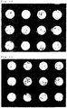
- Fig. 11 it was confirmed that the additive contained in the resin ("additive” is hereinafter referred to also as “convection additive”) had boiled under such a temperature condition that the solder powder melted, and that the bumps were gradually formed well on the round electrodes as the boiling convection additive was convecting within the resin. Therefore, it is suggested that "convection" of the convection additive serves to promote the movement of the molten solder powder, which leads to achievement of a uniform aggregation or agglomeration of the molten solder powder. By contrast, in the case of Fig. 10 , such uniform aggregation or agglomeration of the molten solder powder could not have been achieved due to the absence of the convection additive.
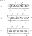
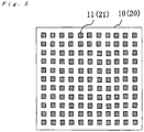
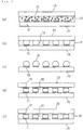
- a resin 13 comprising solder powder (not shown) and a convection additive 12 is supplied onto a wiring substrate 10 having a plurality of electrode terminals 11.
- a semiconductor chip 20 having a plurality of connecting terminals 21 is brought into contact with a surface of the supplied resin 13 such that the connecting terminals 21 of the semiconductor chip 20 are respectively opposed to the electrode terminals 11 of the wiring substrate 10.
- the substrate 10 is heated up to or above a temperature that enables the solder powder to melt.
- the heating step of the wiring substrate 10 is performed at or above a boiling point of the convection additive 12, so that the boiling convection additive 12 is allowed to convect within the resin 13.
- a material capable of boiling at or below a temperature that enables the solder powder to melt e.g., a temperature of from 100 to 300°C or lower temperature
- wax (particularly electron wax or the like) glycerin can be used as the convection additive.
- the convection additive can boil slightly below the melting point of the solder powder, and preferably it boils at a temperature lower than the melting point of the solder powder by from 10 to 100°C, and more preferably by from 10 to 60°C.
- the boiling point of the convection additive may be substantially the same as the melting point of the solder powder.
- the convection additive may boils slightly above the melting point of the solder powder, and preferably it may boil at a temperature higher than the melting point of the solder powder by from 10 to 100°C, and more preferably by from 10 to 20°C.
- the resin 13 is pressed by applying a constant pressure to the semiconductor chip 20 while keeping the semiconductor chip 20 in place during the heating step(s) of the wiring substrate 10.
- the solder powder is prevented from being left to remain in the outside region of the connection formed between each electrode terminal 11 of the wiring substrate 10 and each connecting terminal 21 of the semiconductor chip 20.
- the electrode terminals 21 of the semiconductor chip 20 have fine-pitch arrangement, the residual solder powder remaining in such outside region will not only cause a deteriorating of electrical insulating properties at the region between the neighboring electrical connections, but also cause a short-circuit. Therefore, the avoidance of such residual solder powder is crucial for preventing reliability and process yield from being lowered.
- the optimum content of the solder powder can be determined as follows.
- an underfill material 23 is poured into a clearance gap formed between the wiring substrate 10 and the semiconductor chip 20, followed by heating the wiring substrate 10 in order to thermally cure the underfill material 23.
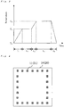
- FIG. 8 shows a top plan view of a wiring substrate 10.
- Figs. 9(a) to 9(c) show cross-sectional views illustrating the steps in the flip chip mounting process.
- the wiring substrate 10 wherein a plurality of electrode terminals 11 are formed in a peripheral region thereof is prepared, the electrode terminals 11 being arranged so as to oppose to peripheral-arranged connecting terminals of the semiconductor chip.
- the resin 13 comprising the solder powder and the convection additive is supplied to the wiring substrate 10 such that the electrode terminals 11 are covered with the supplied resin (see Fig. 9(a) ). This is to say, no resin 13 is supplied to a central region (where no electrode is formed) of the wiring substrate 10.
Landscapes
- Engineering & Computer Science (AREA)
- Manufacturing & Machinery (AREA)
- Microelectronics & Electronic Packaging (AREA)
- Wire Bonding (AREA)
- Electric Connection Of Electric Components To Printed Circuits (AREA)
Claims (7)
- Flip-Chip-Anbringprozess, wobei ein Halbleiterchip mit mehreren Verbindungsanschlüssen einem Verdrahtungssubstrat mit mehreren Elektrodenanschlüssen gegenüber gestellt wird, so dass die Verbindungsanschlüsse elektrisch mit den Elektrodenanschlüssen verbunden sind, wobei der Prozess die Schritte aufweist:(1) Zuführen eines wärmehärtenden Harzes mit Lötpulver und einem Konvektionsadditiv zu einer Oberfläche des Verdrahtungssubstrats, wobei die Oberfläche mit den Elektrodenanschlüssen versehen ist,(2) Inkontaktbringen des Halbleiterchips mit einer Oberfläche des Harzes,(3) Heizen des Verdrahtungssubstrats bis zu einer Temperatur, die dem Lötpulver ermöglicht, zu schmelzen, und dann(4) Heizen des Verdrahtungssubstrats zum Härten des Harzes,wobei in dem Schritt (3) elektrische Verbindungen zwischen den Elektrodenanschlüssen und den Verbindungsanschlüssen gebildet werden und in dem Schritt (4) der Halbleiterchip an dem Verdrahtungssubstrat gesichert wird,
wobei der Schritt (3) des Heizens des Verdrahtungssubstrats bei einer Temperatur ausgeführt wird, die oberhalb eines Siedepunktes des Konvektionsadditivs ist, so dass das Konvektionsadditiv veranlasst wird, zu sieden, und siedendes Konvektionsadditiv, das in einen Gaszustand in dem Harz transformiert ist, das Lötpulver veranlasst, sich zu sammeln, und dem Lötpulver kinetische Energie gibt, so dass sich das Lötpulver in Bereichen zwischen den Elektrodenanschlüssen und den Verbindungsanschlüssen zum Bilden der elektrischen Verbindungen selbst-sammelt. - Flip-Chip-Anbringprozess nach Anspruch 1, wobei in dem Schritt (3) das Lötpulver, das sich in einem geschmolzenen Zustand befindet, innerhalb des Harzes konvektiert.
- Flip-Chip-Anbringprozess nach Anspruch 1, wobei das Konvektionsadditiv wenigstens ein Material ausgewählt aus der Gruppe bestehend aus Glycerin und Wachs ist.
- Flip-Chip-Anbringprozess nach Anspruch 1, wobei der Schritt (3) des Heizens des Verdrahtungssubstrats bei einer Temperatur ausgeführt wird, die ermöglicht, dass sich eine Viskosität des Harzes verringert.
- Flip-Chip-Anbringprozess nach Anspruch 1, wobei das Verdrahtungssubstrat geheizt wird, während das Harz durch Anlegen eines konstanten Druckes auf den Halbleiterchip unter Druck gesetzt wird.
- Flip-Chip-Anbringprozess nach Anspruch 1, wobei der Schritt (4) des Härtens des Harzes ausgeführt wird, indem das Verdrahtungssubstrat zu einer Temperatur oberhalb derer des Schrittes (3) des Heizens des Verdrahtungssubstrats aufgeheizt wird.
- Flip-Chip-Anbringprozess nach Anspruch 1, wobei mehrere Halbleiterchips in Kontakt mit der Oberfläche des Harzes gebracht werden, so dass die mehreren Halbleiterchips über dem Verdrahtungssubstrat Flip-Chip-angebracht werden.
Applications Claiming Priority (3)
| Application Number | Priority Date | Filing Date | Title |
|---|---|---|---|
| JP2004267919 | 2004-09-15 | ||
| JP2005091347A JP3955302B2 (ja) | 2004-09-15 | 2005-03-28 | フリップチップ実装体の製造方法 |
| PCT/JP2005/016423 WO2006030674A1 (ja) | 2004-09-15 | 2005-09-07 | フリップチップ実装方法及びフリップチップ実装体 |
Publications (3)
| Publication Number | Publication Date |
|---|---|
| EP1796156A1 EP1796156A1 (de) | 2007-06-13 |
| EP1796156A4 EP1796156A4 (de) | 2009-10-14 |
| EP1796156B1 true EP1796156B1 (de) | 2017-11-29 |
Family
ID=36059929
Family Applications (1)
| Application Number | Title | Priority Date | Filing Date |
|---|---|---|---|
| EP05782249.6A Expired - Lifetime EP1796156B1 (de) | 2004-09-15 | 2005-09-07 | Flip-chip-anbringverfahren |
Country Status (5)
| Country | Link |
|---|---|
| US (2) | US7759162B2 (de) |
| EP (1) | EP1796156B1 (de) |
| JP (1) | JP3955302B2 (de) |
| KR (1) | KR101179744B1 (de) |
| WO (1) | WO2006030674A1 (de) |
Families Citing this family (41)
| Publication number | Priority date | Publication date | Assignee | Title |
|---|---|---|---|---|
| JP4543899B2 (ja) * | 2004-11-24 | 2010-09-15 | パナソニック株式会社 | フリップチップ実装方法およびフリップチップ実装装置 |
| JP4287475B2 (ja) * | 2004-12-17 | 2009-07-01 | パナソニック株式会社 | 樹脂組成物 |
| JP4405554B2 (ja) * | 2005-03-24 | 2010-01-27 | パナソニック株式会社 | 電子部品の実装方法 |
| CN100495677C (zh) * | 2005-03-29 | 2009-06-03 | 松下电器产业株式会社 | 倒装芯片封装方法及其焊锡点形成方法 |
| JP4084835B2 (ja) * | 2005-03-29 | 2008-04-30 | 松下電器産業株式会社 | フリップチップ実装方法および基板間接続方法 |
| EP1873819A4 (de) * | 2005-04-06 | 2012-07-11 | Panasonic Corp | Flip-chip-anbringverfahren und erhebungsbildungsverfahren |
| JP4402718B2 (ja) * | 2005-05-17 | 2010-01-20 | パナソニック株式会社 | フリップチップ実装方法 |
| KR101257977B1 (ko) * | 2006-03-16 | 2013-04-24 | 파나소닉 주식회사 | 범프형성방법 및 범프형성장치 |
| US7537961B2 (en) * | 2006-03-17 | 2009-05-26 | Panasonic Corporation | Conductive resin composition, connection method between electrodes using the same, and electric connection method between electronic component and circuit substrate using the same |
| US20070238222A1 (en) * | 2006-03-28 | 2007-10-11 | Harries Richard J | Apparatuses and methods to enhance passivation and ILD reliability |
| WO2007122868A1 (ja) * | 2006-03-28 | 2007-11-01 | Matsushita Electric Industrial Co., Ltd. | バンプ形成方法およびバンプ形成装置 |
| DE102006016275B4 (de) * | 2006-03-31 | 2013-12-19 | Asm Assembly Systems Gmbh & Co. Kg | Verfahren zum Platzieren von elektrisch kontaktierbaren Bauelementen auf einem Schaltungsträger |
| KR100793078B1 (ko) * | 2006-06-15 | 2008-01-10 | 한국전자통신연구원 | 플립 칩 패키지 및 그 제조방법 |
| JP5329028B2 (ja) * | 2006-09-15 | 2013-10-30 | パナソニック株式会社 | 電子部品実装構造体の製造方法 |
| WO2008139701A1 (ja) | 2007-04-27 | 2008-11-20 | Panasonic Corporation | 電子部品実装体及びハンダバンプ付き電子部品並びにそれらの製造方法 |
| US7977155B2 (en) * | 2007-05-04 | 2011-07-12 | Taiwan Semiconductor Manufacturing Company, Ltd. | Wafer-level flip-chip assembly methods |
| KR100872711B1 (ko) * | 2007-06-29 | 2008-12-05 | 주식회사 동부하이텍 | 칩적층 구조물 및 이의 제조 방법 |
| US20090057378A1 (en) * | 2007-08-27 | 2009-03-05 | Chi-Won Hwang | In-situ chip attachment using self-organizing solder |
| JP2009186707A (ja) * | 2008-02-06 | 2009-08-20 | Seiko Epson Corp | 電気光学装置の製造方法、電気光学装置 |
| JP5247571B2 (ja) * | 2008-04-24 | 2013-07-24 | パナソニック株式会社 | 配線基板と配線基板の接続方法 |
| JP5264585B2 (ja) | 2009-03-24 | 2013-08-14 | パナソニック株式会社 | 電子部品接合方法および電子部品 |
| KR101208028B1 (ko) | 2009-06-22 | 2012-12-04 | 한국전자통신연구원 | 반도체 패키지의 제조 방법 및 이에 의해 제조된 반도체 패키지 |
| KR101234597B1 (ko) | 2009-10-15 | 2013-02-22 | 한국전자통신연구원 | 플립 칩 본딩 방법 및 그의 구조 |
| JP6008475B2 (ja) * | 2010-07-16 | 2016-10-19 | 大日本印刷株式会社 | 太陽電池モジュールの製造方法 |
| KR101711499B1 (ko) | 2010-10-20 | 2017-03-13 | 삼성전자주식회사 | 반도체 패키지 및 그 제조 방법 |
| US8476115B2 (en) | 2011-05-03 | 2013-07-02 | Stats Chippac, Ltd. | Semiconductor device and method of mounting cover to semiconductor die and interposer with adhesive material |
| TWI612591B (zh) * | 2011-10-26 | 2018-01-21 | 日立化成股份有限公司 | 迴焊薄膜、焊料凸塊形成方法、焊料接合的形成方法及半導體裝置 |
| JP6112797B2 (ja) * | 2012-07-30 | 2017-04-12 | 国立大学法人大阪大学 | 電子部品の実装方法、回路基板の作製方法及び電子部品のはんだ接合部の形成方法、並びに、接続層付きプリント配線板及びシート状接合部材 |
| KR101988890B1 (ko) * | 2012-10-30 | 2019-10-01 | 한국전자통신연구원 | 솔더 온 패드의 제조방법 및 그를 이용한 플립 칩 본딩 방법 |
| US9437566B2 (en) | 2014-05-12 | 2016-09-06 | Invensas Corporation | Conductive connections, structures with such connections, and methods of manufacture |
| US9793198B2 (en) | 2014-05-12 | 2017-10-17 | Invensas Corporation | Conductive connections, structures with such connections, and methods of manufacture |
| KR102411356B1 (ko) | 2014-09-18 | 2022-06-22 | 세키스이가가쿠 고교가부시키가이샤 | 도전 페이스트, 접속 구조체 및 접속 구조체의 제조 방법 |
| US10002843B2 (en) * | 2015-03-24 | 2018-06-19 | Advanced Semiconductor Engineering, Inc. | Semiconductor substrate structure, semiconductor package and method of manufacturing the same |
| JP6769740B2 (ja) * | 2015-05-25 | 2020-10-14 | 積水化学工業株式会社 | 接続構造体の製造方法 |
| KR102569944B1 (ko) | 2015-05-25 | 2023-08-24 | 세키스이가가쿠 고교가부시키가이샤 | 도전 재료 및 접속 구조체 |
| JP7220558B2 (ja) * | 2018-12-26 | 2023-02-10 | エルジー ディスプレイ カンパニー リミテッド | 表示装置及び表示装置の製造方法 |
| US11166384B2 (en) * | 2019-03-20 | 2021-11-02 | Konica Minolta Laboratory U.S.A., Inc. | Fabrication process for flip chip bump bonds using nano-LEDs and conductive resin |
| KR20210001630A (ko) * | 2019-06-28 | 2021-01-06 | 주식회사 노피온 | 자가 조립 및 정렬이 가능한 솔더페이스트를 이용한 마이크로소자 접합방법 |
| JP7145839B2 (ja) * | 2019-12-18 | 2022-10-03 | 株式会社オリジン | はんだ付け基板の製造方法及びはんだ付け装置 |
| TW202214806A (zh) * | 2020-09-30 | 2022-04-16 | 日商太陽油墨製造股份有限公司 | 各向異性導電連接材料及使用各向異性導電連接材料之電子元件的安裝方法 |
| JPWO2024071266A1 (de) * | 2022-09-30 | 2024-04-04 |
Family Cites Families (22)
| Publication number | Priority date | Publication date | Assignee | Title |
|---|---|---|---|---|
| US4611192A (en) * | 1985-01-25 | 1986-09-09 | Eagle Electric Mfg. Co., Inc. | Heavy-duty time-delay fuse |
| JPH0747233B2 (ja) | 1987-09-14 | 1995-05-24 | 古河電気工業株式会社 | 半田析出用組成物および半田析出方法 |
| JPH02251145A (ja) * | 1989-03-24 | 1990-10-08 | Citizen Watch Co Ltd | 突起電極形成方法 |
| JPH06125169A (ja) | 1992-10-13 | 1994-05-06 | Fujitsu Ltd | 予備はんだ法 |
| JPH0927516A (ja) * | 1995-07-12 | 1997-01-28 | Nippondenso Co Ltd | 電子部品の接続構造 |
| AU738424B2 (en) * | 1997-11-19 | 2001-09-20 | Matsushita Electric Industrial Co., Ltd. | Stress relaxation type electronic component, a stress relaxation type circuit board, and a stress relaxation type electronic component mounted member |
| JPH11186334A (ja) * | 1997-12-25 | 1999-07-09 | Toshiba Corp | 半導体実装装置及びその製造方法及び異方性導電材料 |
| JP3996276B2 (ja) | 1998-09-22 | 2007-10-24 | ハリマ化成株式会社 | ソルダペースト及びその製造方法並びにはんだプリコート方法 |
| JP2000332055A (ja) | 1999-05-17 | 2000-11-30 | Sony Corp | フリップチップ実装構造及び実装方法 |
| JP2001093938A (ja) * | 1999-09-20 | 2001-04-06 | Nec Kansai Ltd | 半導体装置及びその製造方法 |
| JP2001329048A (ja) | 2000-03-15 | 2001-11-27 | Harima Chem Inc | 封止充填剤用液状エポキシ樹脂組成物 |
| JP2002026070A (ja) | 2000-07-04 | 2002-01-25 | Toshiba Corp | 半導体装置およびその製造方法 |
| JP3866591B2 (ja) | 2001-10-29 | 2007-01-10 | 富士通株式会社 | 電極間接続構造体の形成方法および電極間接続構造体 |
| JP3996802B2 (ja) * | 2002-05-15 | 2007-10-24 | 太陽インキ製造株式会社 | 低放射線性の光硬化性・熱硬化性樹脂組成物及びその硬化被膜 |
| US20040084206A1 (en) | 2002-11-06 | 2004-05-06 | I-Chung Tung | Fine pad pitch organic circuit board for flip chip joints and board to board solder joints and method |
| JP3769688B2 (ja) | 2003-02-05 | 2006-04-26 | 独立行政法人科学技術振興機構 | 端子間の接続方法及び半導体装置の実装方法 |
| EP1615263A4 (de) | 2003-02-05 | 2006-10-18 | Senju Metal Industry Co | Verfahren zum verbindung von anschlüssen und verfahren zum anbringen eines halbleiterbauelements |
| JP3964911B2 (ja) * | 2004-09-03 | 2007-08-22 | 松下電器産業株式会社 | バンプ付き基板の製造方法 |
| JP4287475B2 (ja) * | 2004-12-17 | 2009-07-01 | パナソニック株式会社 | 樹脂組成物 |
| CN100495677C (zh) * | 2005-03-29 | 2009-06-03 | 松下电器产业株式会社 | 倒装芯片封装方法及其焊锡点形成方法 |
| JP4084835B2 (ja) | 2005-03-29 | 2008-04-30 | 松下電器産業株式会社 | フリップチップ実装方法および基板間接続方法 |
| EP1873819A4 (de) * | 2005-04-06 | 2012-07-11 | Panasonic Corp | Flip-chip-anbringverfahren und erhebungsbildungsverfahren |
-
2005
- 2005-03-28 JP JP2005091347A patent/JP3955302B2/ja not_active Expired - Lifetime
- 2005-09-07 EP EP05782249.6A patent/EP1796156B1/de not_active Expired - Lifetime
- 2005-09-07 WO PCT/JP2005/016423 patent/WO2006030674A1/ja not_active Ceased
- 2005-09-07 US US11/662,286 patent/US7759162B2/en active Active
- 2005-09-07 KR KR1020077005769A patent/KR101179744B1/ko not_active Expired - Lifetime
-
2010
- 2010-03-04 US US12/717,433 patent/US8012801B2/en not_active Expired - Lifetime
Non-Patent Citations (1)
| Title |
|---|
| None * |
Also Published As
| Publication number | Publication date |
|---|---|
| KR101179744B1 (ko) | 2012-09-04 |
| JP3955302B2 (ja) | 2007-08-08 |
| KR20070052791A (ko) | 2007-05-22 |
| US8012801B2 (en) | 2011-09-06 |
| WO2006030674A1 (ja) | 2006-03-23 |
| US7759162B2 (en) | 2010-07-20 |
| EP1796156A4 (de) | 2009-10-14 |
| EP1796156A1 (de) | 2007-06-13 |
| US20100148376A1 (en) | 2010-06-17 |
| US20080017995A1 (en) | 2008-01-24 |
| JP2006114865A (ja) | 2006-04-27 |
Similar Documents
| Publication | Publication Date | Title |
|---|---|---|
| EP1796156B1 (de) | Flip-chip-anbringverfahren | |
| US7799607B2 (en) | Process for forming bumps and solder bump | |
| US7714444B2 (en) | Conductive resin composition, connection method between electrodes using the same, and electric connection method between electronic component and circuit substrate using the same | |
| US7820021B2 (en) | Flip chip mounting method and method for connecting substrates | |
| US7726545B2 (en) | Flip chip mounting process and bump-forming process using electrically-conductive particles as nuclei | |
| US7638883B2 (en) | Flip chip mounting method and bump forming method | |
| US8709293B2 (en) | Flip-chip mounting resin composition and bump forming resin composition | |
| US20030214795A1 (en) | Electronic component with bump electrodes, and manufacturing method thereof | |
| JP5173214B2 (ja) | 導電性樹脂組成物とこれを用いた電極間の接続方法及び電子部品と回路基板の電気接続方法 | |
| KR101421907B1 (ko) | 전자 부품 실장체, 전자 부품 및 기판 | |
| JP4401411B2 (ja) | 半導体チップを備えた実装体およびその製造方法 | |
| CN100442468C (zh) | 倒装片安装方法 | |
| JPH11261210A (ja) | プリント配線基板とチップ部品との接続方法 | |
| JP2000077556A (ja) | ボールグリッドアレイ型半導体装置 | |
| TW201230270A (en) | Semiconductor device and method of forming narrow interconnect sites on substrate with elongated mask openings |
Legal Events
| Date | Code | Title | Description |
|---|---|---|---|
| PUAI | Public reference made under article 153(3) epc to a published international application that has entered the european phase |
Free format text: ORIGINAL CODE: 0009012 |
|
| 17P | Request for examination filed |
Effective date: 20070416 |
|
| AK | Designated contracting states |
Kind code of ref document: A1 Designated state(s): DE FR GB |
|
| DAX | Request for extension of the european patent (deleted) | ||
| RBV | Designated contracting states (corrected) |
Designated state(s): DE FR GB |
|
| RAP1 | Party data changed (applicant data changed or rights of an application transferred) |
Owner name: PANASONIC CORPORATION |
|
| RA4 | Supplementary search report drawn up and despatched (corrected) |
Effective date: 20090914 |
|
| 17Q | First examination report despatched |
Effective date: 20110912 |
|
| RAP1 | Party data changed (applicant data changed or rights of an application transferred) |
Owner name: PANASONIC INTELLECTUAL PROPERTY MANAGEMENT CO., LT |
|
| REG | Reference to a national code |
Ref country code: DE Ref legal event code: R079 Ref document number: 602005053159 Country of ref document: DE Free format text: PREVIOUS MAIN CLASS: H01L0021600000 Ipc: H01L0021560000 |
|
| RIC1 | Information provided on ipc code assigned before grant |
Ipc: H01L 21/56 20060101AFI20170524BHEP Ipc: H01L 21/683 20060101ALI20170524BHEP Ipc: H01L 23/488 20060101ALI20170524BHEP Ipc: H05K 3/34 20060101ALI20170524BHEP Ipc: H01L 21/60 20060101ALI20170524BHEP Ipc: H05K 3/32 20060101ALN20170524BHEP |
|
| GRAP | Despatch of communication of intention to grant a patent |
Free format text: ORIGINAL CODE: EPIDOSNIGR1 |
|
| STAA | Information on the status of an ep patent application or granted ep patent |
Free format text: STATUS: GRANT OF PATENT IS INTENDED |
|
| RIC1 | Information provided on ipc code assigned before grant |
Ipc: H01L 21/56 20060101AFI20170607BHEP Ipc: H05K 3/34 20060101ALI20170607BHEP Ipc: H01L 23/488 20060101ALI20170607BHEP Ipc: H01L 21/683 20060101ALI20170607BHEP Ipc: H01L 21/60 20060101ALI20170607BHEP Ipc: H05K 3/32 20060101ALN20170607BHEP |
|
| RIN1 | Information on inventor provided before grant (corrected) |
Inventor name: TOMEKAWA, SATORU Inventor name: NAKATANI, SEIICHI Inventor name: KITAE, TAKASHI Inventor name: KARASHIMA, SEIJI Inventor name: YAMASHITA, YOSHIHISA |
|
| INTG | Intention to grant announced |
Effective date: 20170703 |
|
| GRAS | Grant fee paid |
Free format text: ORIGINAL CODE: EPIDOSNIGR3 |
|
| GRAA | (expected) grant |
Free format text: ORIGINAL CODE: 0009210 |
|
| STAA | Information on the status of an ep patent application or granted ep patent |
Free format text: STATUS: THE PATENT HAS BEEN GRANTED |
|
| AK | Designated contracting states |
Kind code of ref document: B1 Designated state(s): DE FR GB |
|
| REG | Reference to a national code |
Ref country code: GB Ref legal event code: FG4D |
|
| REG | Reference to a national code |
Ref country code: DE Ref legal event code: R096 Ref document number: 602005053159 Country of ref document: DE |
|
| REG | Reference to a national code |
Ref country code: DE Ref legal event code: R097 Ref document number: 602005053159 Country of ref document: DE |
|
| PLBE | No opposition filed within time limit |
Free format text: ORIGINAL CODE: 0009261 |
|
| STAA | Information on the status of an ep patent application or granted ep patent |
Free format text: STATUS: NO OPPOSITION FILED WITHIN TIME LIMIT |
|
| 26N | No opposition filed |
Effective date: 20180830 |
|
| GBPC | Gb: european patent ceased through non-payment of renewal fee |
Effective date: 20180907 |
|
| PG25 | Lapsed in a contracting state [announced via postgrant information from national office to epo] |
Ref country code: FR Free format text: LAPSE BECAUSE OF NON-PAYMENT OF DUE FEES Effective date: 20180930 |
|
| PG25 | Lapsed in a contracting state [announced via postgrant information from national office to epo] |
Ref country code: GB Free format text: LAPSE BECAUSE OF NON-PAYMENT OF DUE FEES Effective date: 20180907 |
|
| PGFP | Annual fee paid to national office [announced via postgrant information from national office to epo] |
Ref country code: DE Payment date: 20240918 Year of fee payment: 20 |
|
| REG | Reference to a national code |
Ref country code: DE Ref legal event code: R071 Ref document number: 602005053159 Country of ref document: DE |