EP1796202A1 - Circuit de commutation d'haute fréquence et puissance avec chaines de transistors de puissance - Google Patents
Circuit de commutation d'haute fréquence et puissance avec chaines de transistors de puissance Download PDFInfo
- Publication number
- EP1796202A1 EP1796202A1 EP06124121A EP06124121A EP1796202A1 EP 1796202 A1 EP1796202 A1 EP 1796202A1 EP 06124121 A EP06124121 A EP 06124121A EP 06124121 A EP06124121 A EP 06124121A EP 1796202 A1 EP1796202 A1 EP 1796202A1
- Authority
- EP
- European Patent Office
- Prior art keywords
- power
- switch according
- power transistors
- transistors
- mhz
- Prior art date
- Legal status (The legal status is an assumption and is not a legal conclusion. Google has not performed a legal analysis and makes no representation as to the accuracy of the status listed.)
- Granted
Links
Images


Classifications
-
- H—ELECTRICITY
- H01—ELECTRIC ELEMENTS
- H01P—WAVEGUIDES; RESONATORS, LINES, OR OTHER DEVICES OF THE WAVEGUIDE TYPE
- H01P1/00—Auxiliary devices
- H01P1/10—Auxiliary devices for switching or interrupting
- H01P1/15—Auxiliary devices for switching or interrupting by semiconductor devices
-
- H—ELECTRICITY
- H03—ELECTRONIC CIRCUITRY
- H03K—PULSE TECHNIQUE
- H03K17/00—Electronic switching or gating, i.e. not by contact-making and –breaking
- H03K17/06—Modifications for ensuring a fully conducting state
- H03K17/063—Modifications for ensuring a fully conducting state in field-effect transistor switches
-
- H—ELECTRICITY
- H03—ELECTRONIC CIRCUITRY
- H03K—PULSE TECHNIQUE
- H03K2217/00—Indexing scheme related to electronic switching or gating, i.e. not by contact-making or -breaking covered by H03K17/00
- H03K2217/0036—Means reducing energy consumption
Definitions
- This invention relates to electronic circuits, and more particularly to electronic switch circuits.
- Electronic switch circuits are widely used to switch high power (for example, at least 20 watts) at high frequencies (for example in the range of MHz and beyond).
- Semiconductor device manufacturers have developed transistors that are capable of operating at high frequencies and are still capable of handling higher power loads.
- MOSFETs metal semiconductor field effect transistors
- High power, high frequency MESFETs have been fabricated from semiconductor materials including gallium arsenide, silicon carbide and/or gallium nitride.
- one or more power transistors such as MESFETs, are connected into a circuit. It is desirable for such circuits to have a high power handling ability over a range of high frequencies, to provide relatively large isolation of the high power signal when in the "off” state, and relatively low resistance when in the "on” state.
- High power, high frequency switches include a transmission line having at least three portions that are serially coupled between an input port and an output port, to define at least two nodes therebetween, and to carry a high power, high frequency signal between the input port and the output port.
- First and second power transistors are provided, each including a controlling electrode and controlled electrodes.
- At least a third power transistor is also provided, including a controlling electrode and controlled electrodes.
- the controlled electrodes of a respective one of the first and second power transistors and of a respective one of the at least a third power transistor are serially coupled between a respective one of the at least two nodes and a reference voltage.
- the controlling electrodes of the first, second and/or at least a third power transistor are responsive to a switch control input.
- the first, second and the at least a third power transistor are operable to shunt the first and second nodes to the reference voltage, and to decouple from the nodes, in response to the switch control signal.
- the at least a third power transistor comprises a third and a fourth power transistor.
- the controlled electrodes of the first and third power transistors are serially connected between the first node and the reference voltage, and the controlled electrodes of the second and fourth power transistors are serially connected between the second node and the reference voltage.
- the at least a third power transistor consists of a third power transistor.
- the controlled electrodes of a respective one of the first and second power transistors and the third power transistor are serially coupled between the respective one of the at least two nodes and the reference voltage.
- the transmission line comprises an actual transmission line including the at least three portions.
- the transmission line may include strip lines, coaxial lines and/or other conventional transmission lines.
- the transmission line comprises an artificial transmission line that is formed of, for example, distributed series inductors and distributed shunt capacitors.
- the shunt capacitors comprise parasitic capacitance of the first and second power transistors.
- High power, high frequency switches include a signal line that carries a high power, high frequency signal between an input port and an output port, and a plurality of strings of serially connected power transistors.
- a respective string of serially connected power transistors is connected between the signal line and a reference voltage, and is responsive to a switch control signal.
- the plurality of strings of serially connected power transistors are operable to shunt to the signal line to the reference voltage, and to decouple from the signal line, in response to the switch control signal.
- the above-described power transistors are embodied as silicon carbide MESFETs.
- the above-described circuits are configured to provide at least 50 watts of power handling at less than 0.25 dB compression, an isolation of at least 32 dB and an effective on resistance of less than 0.5 ohm over a frequency range of from about 20 MHz to about 200 MHz.
- the above-described circuits are configured to provide at least 50 watts of power handling at less than 0.3 dB compression, an isolation of at least 45 dB and an effective on resistance of less than 0.5 ohm over a frequency range from about 500 MHz to about 1000 MHz.
- Figure 1 is a block diagram of a high power, high frequency switch according to various embodiments of the present invention.
- FIGS 2 and 3 are circuit diagrams of high power, high frequency switches according to various embodiments of the present invention.
- Figure 4 is a circuit simulation of a high power, high frequency switch according to some embodiments of the present invention in the "on" state.
- Figures 5-8 graphically illustrate simulation results for the circuit of Figure 4.
- Figure 9 is a circuit simulation of a high power, high frequency switch according to some embodiments of the present invention in the "off" state.
- FIGS 10-13 graphically illustrate simulation results for the circuit of Figure 9.
- Figure 14 is a circuit simulation of a high power, high frequency switch according to other embodiments of the present invention in the "on" state.
- FIGS 15-18 graphically illustrate simulation results for the circuit of Figure 14.
- Figure 19 is a circuit simulation of a high power, high frequency switch according to other embodiments of the present invention in the "off" state.
- FIGS 20-23 graphically illustrate simulation results for the circuit of Figure 19.
- Figure 24 is a circuit simulation of a single pole/double throw switch according to other embodiments of the present invention.
- first, second, etc. may be used herein to describe various elements, these elements should not be limited by these terms. These terms are only used to distinguish one element from another. For example, a first transistor could be termed a second transistor, and, similarly, a second transistor could be termed a first transistor without departing from the teachings of the disclosure.
- FIG. 1 is a block diagram of a high power, high frequency switch according to various embodiments of the present invention.
- these embodiments of high power, high frequency switch 100 include a transmission line 110 including at least three transmission line portions 112a-112c that are serially coupled between an input port 120 and an output port 130 to define at least two nodes 114a, 114b therebetween.
- the transmission line portions 112a-112e are also labeled TLP1-TLP3 in Figure 1.
- the transmission line 110 carries the high power, high frequency signal between the input port 120 and the output port 130, in either or both directions.
- first and second power transistors 140, 142 respectively, include a controlling electrode, such as a gate or base, and controlled electrodes, such as source/drain or emitter/collector electrodes.
- At least a third power transistor 150 is also provided, including a controlling electrode and controlled electrodes.
- the controlled electrodes of a respective one of the first and second transistors 140, 142, and of a respective one of the at least a third transistor 150 are serially coupled between a respective one of the at least two nodes 114a, 114b, and a reference voltage, shown as ground voltage.
- the serial coupling of a respective power transistor 140, 142 to a respective node 114a, 114b is indicated by respective connections 140a, 142a.
- the respective serial coupling between a controlled electrode of the first and second power transistors 140, 142 with the at least a third power transistor 150 is indicated by the connections 140b, 142b in Figure 1.
- the controlling electrodes of the first power transistor 140, second power transistor 142 and/or at least a third power transistor 150 is responsive to a switch control input 160.
- the controlling electrodes of the at least a third power transistor 150 are responsive to the switch control input 160 .
- the controlling electrodes of the first power transistor 140 and/or second power transistor 142 is responsive to the switch control input.
- the first power transistor 140, second power transistor 142 and at least a third power transistor 150 are all responsive to the switch control input 160.
- a given power transistor may be directly responsive to the switch control input 160 or may be indirectly responsive to the switch control input 160, for example by way of a voltage divider or other circuit.
- FIG. 2 is a circuit diagram of a high power, high frequency switch according to other embodiments of the present invention.
- the transmission line 110' comprises an artificial transmission line that includes distributed series inductors 212a-212c, and distributed shunt capacitors.
- the distributed shunt capacitors may be provided by the parasitic capacitance of the first and second power transistors 140', 142', by parasitic capacitances of the interconnections 140a', 142a' and/or by discrete capacitors.
- the first and second power transistors 140', 142' are metal semiconductor field effect transistors (MESFETs) and, in some embodiments, silicon carbide-based MESFETS.
- MESFETs metal semiconductor field effect transistors
- the at least a third power transistor 150 of Figure 1 comprises a third power transistor 250 and a fourth power transistor 252.
- the third and fourth power transistors 250, 252 include controlling electrodes (gates) that are responsive to the switch control input.
- the controlled electrodes (source/drain) of the first and third power transistors 140' and 250 are serially connected between the first node 114a and the reference voltage (here ground), as shown by the connections 140a', 140b'.
- the controlled electrodes of the second and fourth power transistors 142', 252 are serially connected between the second node 114b and the reference voltage, as shown by the connections 142a', 142b'.
- the third and fourth power transistors may also be embodied as MESFETs and, in some embodiments, as silicon carbide-based MESFETs.
- Figure 3 illustrates yet other embodiments of the present invention.
- the transmission line 110" comprises an actual transmission line including at least three transmission lines 312a, 312b, 312c.
- Discrete shunt capacitors 314a, 314b may also be provided.
- the at least a third power transistor 150 of Figure 1 consists of a single power transistor 350 including a controlling electrode that is responsive to the switch control input 160 .
- the controlled electrodes of a respective one of the first and second transistors 140', 142' and of the third transistor 350 are serially coupled between a respective one of the at least two nodes 114a, 114b and the reference voltage, here ground.
- FIG. 1 It will be understood by those having skill in the art that various embodiments of Figures 1-3 may be combined in various combinations and subcombinations. For example, a single third power transistor 350 and/or multiple third power transistors 250, 252 may be used with any of the embodiments. Moreover, an artificial transmission line 110' and/or an actual transmission line 110" may be used with any of the embodiments.
- the switch control input 160 may also be connected to the first and second power transistors 140, 142, 140', 142' directly and/or via a resistive divider or other circuit.
- the first, second and at least a third power transistors are operable to shunt the first and second nodes 114a, 114b to the reference voltage, such as ground, and to decouple from the nodes 114a, 114b , in response to the switch control input 160 .
- High power, high frequency switches may also be regarded as including a signal line 110, 110', 110" that carries a high power, high frequency signal between an input port 120 and an output port 130.
- a plurality of strings 170a, 170b (Figure 1); 170a', 170b' ( Figure 2); and 170a", 170b" ( Figure 3) are provided, a respective one of which is connected between the signal line 110, 110', 110" and the reference voltage, and which are responsive to a switch control signal 160.
- the strings may include independent transistors, as illustrated in Figure 2, or a given transistor may be shared by two or more strings, as illustrated in Figure 3.
- embodiments of Figures 1-3 include only two transistors in a given string. However, three or more transistors also may be stacked in a given string. Finally, only two strings are shown in Figures 1-3. However, more than two strings may also be provided in other embodiments of the present invention.
- the power transistors of Figures 1-3 may be embodied by MESFETs and, in some embodiments, by silicon carbide MESFETs.
- Silicon carbide MESFETs are known to those having skill in the art and are described, for example, in U.S. Patents 4,762,806 ; 4,757,028 ; 5,270,554 ; 5,925,895 ; 6,686,616 ; 6,906,350 and 6,956,239 .
- devices such as those described in U.S. Patent Application Serial No. 10/977,054, filed on October 29, 2004 entitled Metal-Semiconductor Field Effect Transistors (MESFETs) Having Drains Coupled to the Substrate and Methods of Fabricating the Same; Serial No.
- Gallium arsenide (GaAs) MESFETs and/or gallium nitride (GaN) MESFETs may be used.
- MESFETs formed of two or more of these materials also may be used.
- HEMTs High Electron Mobility Transistors
- MODFETs Modulation-Doped Field Effect Transistors
- HEMTs as described in U.S. Patents 5,192,987 ; 5,296,395 ; 6,316,793 ; 6,548,333 ; and 6,849,882 may be used.
- Other suitable structures for gallium nitride-based HEMTs are described, for example, in U.S. Patent Publication No. 2004/0061129 filed July 11, 2003 and published April 1, 2004 for Nitride-Based Transistors And Methods Of Fabrication Thereof Using Non-Etched Contact Recesses; U.S.
- Patent Publication No. 2003/0020092 filed July 23, 2002 and published January 30, 2003 for Insulating Gate AlGaN / GaN HEMT ;
- some embodiments of the invention can employ pairs of silicon carbide MESFETs in an artificial/actual transmission line configuration, such that the drain and gate voltages on the MESFETs are changed to provide a low loss (or even some gain) "on" state or a high isolation “off” state.
- Stacked MESFETs may be used to increase or maximize radio frequency (RF) power handling ability at low frequencies, by providing the voltage swing across the gates of the devices.
- RF radio frequency
- Suitable gate width FETs may be used to enable RF power handling with low compression.
- Some embodiments of the invention can provide a high power, high isolation switch covering a decade of bandwidth at relatively low current drive.
- Embodiments of the invention may also be compatible with standard Monolithic Microwave Integrated Circuit (MMIC) design practices, which can allow the potential integration of the switch configurations of embodiments of the present invention with other circuit elements, such as power amplifiers.
- MMIC Monolithic Microwave Integrated Circuit
- switches for the same levels of RF power handling capacities may employ PIN diodes, which may draw large amounts of current in their "on" states and may not be compatible with MMIC technology.
- some embodiments of the invention can use multiple FETs in an actual/artificial transmission line configuration and/or may employ stacked transistors to allow greater power handling capability, particularly at low frequencies, where the low parasitic capacitance of the transistors may not contribute to the effective voltage division between the gate and drain, and the gate and source.
- Some embodiments of the present invention can provide a 20 MHz to 200 MHz single pole/single throw switch. Moreover, other embodiments of the invention can be scaled in power handling and/or frequency, to cover specific bandwidths.
- the single pole/single throw switch configuration also may provide a building block for many other switch configurations, such as multiple pole/multiple throw switches.
- Embodiments of the invention can exhibit well behaved compression characteristics in the "on" state, where simulations indicate only 0.2 dB loss at 56 watts continuous wave power, as described below. Low switch loss at high power levels can be used to reduce or minimize dissipated power/heat, increase or maximize system efficiency, etc.
- Other embodiments of the present invention can replace the series inductors of Figure 2 with actual transmission lines, as in Figure 3. Actual transmission lines may be used in higher frequency applications, in some embodiments of the present invention.
- the transmission line 110, 110', 110" and the first, second and at least the third transistors 140, 142, 150 may be configured to provide at least 50 watts of power handling at less than 0.25 dB compression, an isolation of at least 32 dB and an effective on resistance of less than 0.5 ohm over a frequency range from about 20 MHz to about 200 MHz.
- At least 50 watts of power handling is provided at less than 0.3 dB compression, an isolation of about 45 dB and an effective "on"resistance of less than 0.5 ohm over a frequency range from about 500 MHz to about 1000 MHz.
- Figures 4-13 refer to a first high power, high frequency switch according to exemplary embodiments of the present invention. These embodiments are capable of more than 50 watts power handling at less than 0.25 dB compression. An isolation of at least 32 dB is provided over a bandwidth from about 20 MHz to about 200 MHz. The effective"on"resistance is less than about 0.5 ohm. These embodiments are implemented using an artificial transmission line with two pairs of silicon carbide MESFETs, to absorb the drain-to-source capacitance in shunt mode approach, as was illustrated schematically in Figure 2. In some embodiments, stacked bare die silicon carbide MESFETs may be used to increase or maximize power handling ability at low frequencies.
- Figure 4 illustrates a circuit simulation of the switch in the "on" state. Like numbers with Figure 2 are used. DC blocking capacitors 420a, 420b are also shown. A switch control input voltage of -20 V and a power supply voltage of 70 V are shown. Parasitic inductors are also shown for purposes of the simulation.
- Figure 5 graphically illustrates simulated small signal insertion loss in the "on" state for the MESFET switch of Figure 3. As shown, a loss of less than 0.25 dB is shown for frequencies between 20 MHz and 200 MHz.
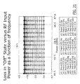
- Figure 6 illustrates simulated loss in the "on” state versus RF input power as a function of frequency.
- Figure 7 illustrates simulated DC current in the "on” state versus RF input power and frequency.
- Figure 8 illustrates the simulated voltage at the stacked FET nodes in the switch "on” state. In other words, Figure 8 illustrates that the voltage across the first and second power transistors 140', 142' are less than 50 volts between drain and source.
- Figure 9 is a circuit simulation of the switch of Figure 4 in the "off' state, where the power supply voltage VDD is switched to 0 V and the gate-to-source voltage corresponding to the switch control input 160 is switched to 2 V.
- Figure 10 graphically illustrates simulated small signal insertion loss in the "off' state
- Figure 11 illustrates simulated loss in the "off” state versus RF input power as a function of frequency.
- Figure 12 illustrates simulated DC current in the "off” state versus RF input power and frequency.
- Figure 13 illustrates the simulated voltage at the stacked FET nodes in the switch "off” state.
- Figures 4-13 show that some embodiments of the present invention that can provide at least 50 watts of power handling at less than 0.25 dB compression, an isolation of at least 32 dB and an effective on resistance of at least 0.5 ohm over a frequency range from about 20 MHz to about 200 MHz.
- Figures 14-23 refer to a second embodiment of a high power, high frequency silicon carbide MESFET switch that is capable of at least 50 watts power handling at less than about 0.3 dB compression, an isolation of at least 45 dB and an effective on resistance of less than 0.5 ohm over a frequency range of from about 500 MHz to about 1000 MHz.
- This embodiment was implemented using actual transmission lines 110" and shunt capacitors 314a, 314b, as was illustrated in Figure 3, but with two pairs of FETs 140', 250; and 142', 252 to absorb drain-to-source capacitance in shunt mode approach, as was illustrated in Figure 2. Stacked bare die FETs may be used to increase or maximize power handling.
- Figure 14 illustrates this embodiment in the "on” state. Like numbers with Figures 2 and 3 are used. In the "on” state, a power supply voltage of 70 V and a control signal voltage 160 of -15 V is used.
- Figure 15 illustrates the simulated small signal insertion loss in the "on" state which is shown to be less than about 0.3 dB.
- Figure 16 illustrates simulated loss in the "on” state versus RF input power as a function of frequency.
- Figure 17 illustrates simulated DC current in the "on” state versus RF input power and frequency.
- Figure 18 illustrates simulated voltage at the stacked FET nodes in the "on” state, and shows voltage across the grounded gate FETs of less than 50 volts.
- Figure 19 shows the embodiment of Figure 14 in the "off" state, where a power supply voltage of 0 V and a control signal voltage of 2 V is provided.
- Figure 20 graphically illustrates simulated small signal insertion loss in the "off” state.
- Figure 21 illustrates simulated loss in the "off” state versus RF input power as a function of frequency.
- Figure 22 illustrates simulated DC current in the "off” state versus RF input power and frequency.
- Figure 23 illustrates simulated voltage at the stacked FET nodes in the switch "off' state.
- Figures 14-23 show that some embodiments of the invention can provide at least 50 watts of power handling at less than 0.3 dB compression, an isolation of at least 45 dB, and an effective on resistance of less than 0.5 ohm over a frequency range from about 500 MHz to about 1000 MHz.
- embodiments of the present invention have been described above in connection with single pole/single throw switches. However, embodiments of the present invention can be used for more complex switches with more poles/throws, such as a single pole/double throw switch.
- a schematic diagram of a simulated single pole/double throw switch is illustrated in Figure 24.
Landscapes
- Electronic Switches (AREA)
Applications Claiming Priority (1)
| Application Number | Priority Date | Filing Date | Title |
|---|---|---|---|
| US11/295,060 US7368971B2 (en) | 2005-12-06 | 2005-12-06 | High power, high frequency switch circuits using strings of power transistors |
Publications (2)
| Publication Number | Publication Date |
|---|---|
| EP1796202A1 true EP1796202A1 (fr) | 2007-06-13 |
| EP1796202B1 EP1796202B1 (fr) | 2013-07-10 |
Family
ID=37806956
Family Applications (1)
| Application Number | Title | Priority Date | Filing Date |
|---|---|---|---|
| EP06124121.2A Active EP1796202B1 (fr) | 2005-12-06 | 2006-11-15 | Circuit de commutation d'haute fréquence et puissance avec chaines de transistors de puissance |
Country Status (2)
| Country | Link |
|---|---|
| US (1) | US7368971B2 (fr) |
| EP (1) | EP1796202B1 (fr) |
Families Citing this family (9)
| Publication number | Priority date | Publication date | Assignee | Title |
|---|---|---|---|---|
| FR2931300B1 (fr) * | 2008-05-16 | 2016-10-21 | Thales Sa | Commutateur hyperfrequence et module d'emission et de reception comportant un tel commutateur |
| US7764120B2 (en) * | 2008-08-19 | 2010-07-27 | Cree, Inc. | Integrated circuit with parallel sets of transistor amplifiers having different turn on power levels |
| US7893791B2 (en) | 2008-10-22 | 2011-02-22 | The Boeing Company | Gallium nitride switch methodology |
| US8390395B2 (en) | 2010-05-03 | 2013-03-05 | Raytheon Company | High power RF switch with active device size tapering |
| US8421122B2 (en) * | 2010-05-20 | 2013-04-16 | Cree, Inc. | High power gallium nitride field effect transistor switches |
| US9065426B2 (en) | 2011-11-03 | 2015-06-23 | Advanced Energy Industries, Inc. | High frequency solid state switching for impedance matching |
| US8436643B2 (en) | 2010-11-04 | 2013-05-07 | Advanced Energy Industries, Inc. | High frequency solid state switching for impedance matching |
| US10027366B2 (en) * | 2014-04-25 | 2018-07-17 | Raytheon Company | High power radio frequency (RF) antenna switch |
| US12087770B2 (en) | 2021-08-05 | 2024-09-10 | International Business Machines Corporation | Complementary field effect transistor devices |
Citations (3)
| Publication number | Priority date | Publication date | Assignee | Title |
|---|---|---|---|---|
| US5666089A (en) | 1996-04-12 | 1997-09-09 | Hewlett-Packard Company | Monolithic step attenuator having internal frequency compensation |
| US5990580A (en) * | 1998-03-05 | 1999-11-23 | The Whitaker Corporation | Single pole double throw switch |
| US20030132814A1 (en) * | 2002-01-15 | 2003-07-17 | Nokia Corporation | Circuit topology for attenuator and switch circuits |
Family Cites Families (17)
| Publication number | Priority date | Publication date | Assignee | Title |
|---|---|---|---|---|
| US4762806A (en) * | 1983-12-23 | 1988-08-09 | Sharp Kabushiki Kaisha | Process for producing a SiC semiconductor device |
| JP2615390B2 (ja) * | 1985-10-07 | 1997-05-28 | 工業技術院長 | 炭化シリコン電界効果トランジスタの製造方法 |
| US5081706A (en) * | 1987-07-30 | 1992-01-14 | Texas Instruments Incorporated | Broadband merged switch |
| US4929855A (en) * | 1988-12-09 | 1990-05-29 | Grumman Corporation | High frequency switching device |
| US5012123A (en) * | 1989-03-29 | 1991-04-30 | Hittite Microwave, Inc. | High-power rf switching system |
| US5192987A (en) * | 1991-05-17 | 1993-03-09 | Apa Optics, Inc. | High electron mobility transistor with GaN/Alx Ga1-x N heterojunctions |
| US5270554A (en) * | 1991-06-14 | 1993-12-14 | Cree Research, Inc. | High power high frequency metal-semiconductor field-effect transistor formed in silicon carbide |
| US5925895A (en) * | 1993-10-18 | 1999-07-20 | Northrop Grumman Corporation | Silicon carbide power MESFET with surface effect supressive layer |
| JPH0927736A (ja) * | 1995-07-13 | 1997-01-28 | Japan Radio Co Ltd | Fetスイッチ |
| US6316793B1 (en) * | 1998-06-12 | 2001-11-13 | Cree, Inc. | Nitride based transistors on semi-insulating silicon carbide substrates |
| US6686616B1 (en) * | 2000-05-10 | 2004-02-03 | Cree, Inc. | Silicon carbide metal-semiconductor field effect transistors |
| US6548333B2 (en) * | 2000-12-01 | 2003-04-15 | Cree, Inc. | Aluminum gallium nitride/gallium nitride high electron mobility transistors having a gate contact on a gallium nitride based cap segment |
| US6849882B2 (en) * | 2001-05-11 | 2005-02-01 | Cree Inc. | Group-III nitride based high electron mobility transistor (HEMT) with barrier/spacer layer |
| CN1557024B (zh) * | 2001-07-24 | 2010-04-07 | 美商克立股份有限公司 | 绝缘栅铝镓氮化物/氮化钾高电子迁移率晶体管(hemt) |
| US6906350B2 (en) * | 2001-10-24 | 2005-06-14 | Cree, Inc. | Delta doped silicon carbide metal-semiconductor field effect transistors having a gate disposed in a double recess structure |
| US6982204B2 (en) * | 2002-07-16 | 2006-01-03 | Cree, Inc. | Nitride-based transistors and methods of fabrication thereof using non-etched contact recesses |
| US6956239B2 (en) * | 2002-11-26 | 2005-10-18 | Cree, Inc. | Transistors having buried p-type layers beneath the source region |
-
2005
- 2005-12-06 US US11/295,060 patent/US7368971B2/en not_active Expired - Lifetime
-
2006
- 2006-11-15 EP EP06124121.2A patent/EP1796202B1/fr active Active
Patent Citations (3)
| Publication number | Priority date | Publication date | Assignee | Title |
|---|---|---|---|---|
| US5666089A (en) | 1996-04-12 | 1997-09-09 | Hewlett-Packard Company | Monolithic step attenuator having internal frequency compensation |
| US5990580A (en) * | 1998-03-05 | 1999-11-23 | The Whitaker Corporation | Single pole double throw switch |
| US20030132814A1 (en) * | 2002-01-15 | 2003-07-17 | Nokia Corporation | Circuit topology for attenuator and switch circuits |
Non-Patent Citations (1)
| Title |
|---|
| UMEDA Y ET AL INSTITUTE OF ELECTRICAL AND ELECTRONICS ENGINEERS: "Novel direct-coupled current switch architecture for a series-connected voltage-balancing pulse driver", 2003 IEEE MTT-S INTERNATIONAL MICROWAVE SYMPOSIUM DIGEST.(IMS 2003). PHILADELPHIA, PA, JUNE 8 - 13, 2003, IEEE MTT-S INTERNATIONAL MICROWAVE SYMPOSIUM, NEW YORK, NY : IEEE, US, vol. VOL. 3 OF 3, 8 June 2003 (2003-06-08), pages 2265 - 2268, XP010746706, ISBN: 0-7803-7695-1 * |
Also Published As
| Publication number | Publication date |
|---|---|
| US7368971B2 (en) | 2008-05-06 |
| US20070126492A1 (en) | 2007-06-07 |
| EP1796202B1 (fr) | 2013-07-10 |
Similar Documents
| Publication | Publication Date | Title |
|---|---|---|
| US9742400B2 (en) | System and method for driving radio frequency switch | |
| US8421122B2 (en) | High power gallium nitride field effect transistor switches | |
| US7561853B2 (en) | Radio frequency switch | |
| US11990874B2 (en) | Device stack with novel gate capacitor topology | |
| US20010040479A1 (en) | Electronic switch | |
| US7893749B2 (en) | High frequency switch circuit having reduced input power distortion | |
| US8614597B2 (en) | High linear voltage variable attenuator (VVA) | |
| US5945879A (en) | Series-connected microwave power amplifiers with voltage feedback and method of operation for the same | |
| CN109792234A (zh) | 堆叠晶体管放大器的本体连结优化 | |
| US11323072B1 (en) | Mixer with series connected active devices | |
| CN107408942A (zh) | 具有分布式开关的射频切换电路 | |
| CN119675648A (zh) | 用于射频应用的转移印刷 | |
| EP1796202B1 (fr) | Circuit de commutation d'haute fréquence et puissance avec chaines de transistors de puissance | |
| JP5011312B2 (ja) | 高電力スイッチングのための方法及びシステム | |
| Huang et al. | A 20-mW G-band monolithic driver amplifier using 0.07-μm InP HEMT | |
| Dennler et al. | Monolithic three-stage 6–18GHz high power amplifier with distributed interstage in GaN technology | |
| CN107078722B (zh) | 具有射频扼流圈的有源环流器 | |
| US6774416B2 (en) | Small area cascode FET structure operating at mm-wave frequencies | |
| US9641156B1 (en) | Active circulator with cascode transistor | |
| Campbell et al. | Design considerations for GaN based MMICs | |
| US20110204966A1 (en) | Transistor junction diode circuitry systems and methods | |
| Koudymov et al. | Monolithically integrated high-power broad-band RF switch based on III-N insulated gate transistors | |
| US20090079489A1 (en) | Constant phase digital attenuator with on-chip matching circuitry | |
| US11451226B2 (en) | Radio frequency switch circuitry | |
| US10177741B1 (en) | Envelope tracking active circulator |
Legal Events
| Date | Code | Title | Description |
|---|---|---|---|
| PUAI | Public reference made under article 153(3) epc to a published international application that has entered the european phase |
Free format text: ORIGINAL CODE: 0009012 |
|
| AK | Designated contracting states |
Kind code of ref document: A1 Designated state(s): AT BE BG CH CY CZ DE DK EE ES FI FR GB GR HU IE IS IT LI LT LU LV MC NL PL PT RO SE SI SK TR |
|
| AX | Request for extension of the european patent |
Extension state: AL BA HR MK YU |
|
| 17P | Request for examination filed |
Effective date: 20071203 |
|
| 17Q | First examination report despatched |
Effective date: 20080109 |
|
| AKX | Designation fees paid |
Designated state(s): AT BE BG CH CY CZ DE DK EE ES FI FR GB GR HU IE IS IT LI LT LU LV MC NL PL PT RO SE SI SK TR |
|
| GRAP | Despatch of communication of intention to grant a patent |
Free format text: ORIGINAL CODE: EPIDOSNIGR1 |
|
| GRAP | Despatch of communication of intention to grant a patent |
Free format text: ORIGINAL CODE: EPIDOSNIGR1 |
|
| GRAP | Despatch of communication of intention to grant a patent |
Free format text: ORIGINAL CODE: EPIDOSNIGR1 |
|
| GRAP | Despatch of communication of intention to grant a patent |
Free format text: ORIGINAL CODE: EPIDOSNIGR1 |
|
| INTG | Intention to grant announced |
Effective date: 20130424 |
|
| GRAS | Grant fee paid |
Free format text: ORIGINAL CODE: EPIDOSNIGR3 |
|
| GRAA | (expected) grant |
Free format text: ORIGINAL CODE: 0009210 |
|
| INTG | Intention to grant announced |
Effective date: 20130514 |
|
| AK | Designated contracting states |
Kind code of ref document: B1 Designated state(s): AT BE BG CH CY CZ DE DK EE ES FI FR GB GR HU IE IS IT LI LT LU LV MC NL PL PT RO SE SI SK TR |
|
| REG | Reference to a national code |
Ref country code: GB Ref legal event code: FG4D |
|
| REG | Reference to a national code |
Ref country code: AT Ref legal event code: REF Ref document number: 621418 Country of ref document: AT Kind code of ref document: T Effective date: 20130715 Ref country code: CH Ref legal event code: EP |
|
| REG | Reference to a national code |
Ref country code: IE Ref legal event code: FG4D |
|
| REG | Reference to a national code |
Ref country code: DE Ref legal event code: R096 Ref document number: 602006037202 Country of ref document: DE Effective date: 20130905 |
|
| PG25 | Lapsed in a contracting state [announced via postgrant information from national office to epo] |
Ref country code: SI Free format text: LAPSE BECAUSE OF FAILURE TO SUBMIT A TRANSLATION OF THE DESCRIPTION OR TO PAY THE FEE WITHIN THE PRESCRIBED TIME-LIMIT Effective date: 20130710 |
|
| REG | Reference to a national code |
Ref country code: AT Ref legal event code: MK05 Ref document number: 621418 Country of ref document: AT Kind code of ref document: T Effective date: 20130710 |
|
| REG | Reference to a national code |
Ref country code: NL Ref legal event code: VDEP Effective date: 20130710 |
|
| REG | Reference to a national code |
Ref country code: LT Ref legal event code: MG4D |
|
| PG25 | Lapsed in a contracting state [announced via postgrant information from national office to epo] |
Ref country code: CY Free format text: LAPSE BECAUSE OF FAILURE TO SUBMIT A TRANSLATION OF THE DESCRIPTION OR TO PAY THE FEE WITHIN THE PRESCRIBED TIME-LIMIT Effective date: 20130717 Ref country code: IS Free format text: LAPSE BECAUSE OF FAILURE TO SUBMIT A TRANSLATION OF THE DESCRIPTION OR TO PAY THE FEE WITHIN THE PRESCRIBED TIME-LIMIT Effective date: 20131110 Ref country code: SE Free format text: LAPSE BECAUSE OF FAILURE TO SUBMIT A TRANSLATION OF THE DESCRIPTION OR TO PAY THE FEE WITHIN THE PRESCRIBED TIME-LIMIT Effective date: 20130710 Ref country code: PT Free format text: LAPSE BECAUSE OF FAILURE TO SUBMIT A TRANSLATION OF THE DESCRIPTION OR TO PAY THE FEE WITHIN THE PRESCRIBED TIME-LIMIT Effective date: 20131111 Ref country code: AT Free format text: LAPSE BECAUSE OF FAILURE TO SUBMIT A TRANSLATION OF THE DESCRIPTION OR TO PAY THE FEE WITHIN THE PRESCRIBED TIME-LIMIT Effective date: 20130710 Ref country code: LT Free format text: LAPSE BECAUSE OF FAILURE TO SUBMIT A TRANSLATION OF THE DESCRIPTION OR TO PAY THE FEE WITHIN THE PRESCRIBED TIME-LIMIT Effective date: 20130710 Ref country code: BE Free format text: LAPSE BECAUSE OF FAILURE TO SUBMIT A TRANSLATION OF THE DESCRIPTION OR TO PAY THE FEE WITHIN THE PRESCRIBED TIME-LIMIT Effective date: 20130710 |
|
| PG25 | Lapsed in a contracting state [announced via postgrant information from national office to epo] |
Ref country code: NL Free format text: LAPSE BECAUSE OF FAILURE TO SUBMIT A TRANSLATION OF THE DESCRIPTION OR TO PAY THE FEE WITHIN THE PRESCRIBED TIME-LIMIT Effective date: 20130710 Ref country code: GR Free format text: LAPSE BECAUSE OF FAILURE TO SUBMIT A TRANSLATION OF THE DESCRIPTION OR TO PAY THE FEE WITHIN THE PRESCRIBED TIME-LIMIT Effective date: 20131011 Ref country code: ES Free format text: LAPSE BECAUSE OF FAILURE TO SUBMIT A TRANSLATION OF THE DESCRIPTION OR TO PAY THE FEE WITHIN THE PRESCRIBED TIME-LIMIT Effective date: 20131021 Ref country code: LV Free format text: LAPSE BECAUSE OF FAILURE TO SUBMIT A TRANSLATION OF THE DESCRIPTION OR TO PAY THE FEE WITHIN THE PRESCRIBED TIME-LIMIT Effective date: 20130710 Ref country code: PL Free format text: LAPSE BECAUSE OF FAILURE TO SUBMIT A TRANSLATION OF THE DESCRIPTION OR TO PAY THE FEE WITHIN THE PRESCRIBED TIME-LIMIT Effective date: 20130710 |
|
| PG25 | Lapsed in a contracting state [announced via postgrant information from national office to epo] |
Ref country code: CY Free format text: LAPSE BECAUSE OF FAILURE TO SUBMIT A TRANSLATION OF THE DESCRIPTION OR TO PAY THE FEE WITHIN THE PRESCRIBED TIME-LIMIT Effective date: 20130710 |
|
| PG25 | Lapsed in a contracting state [announced via postgrant information from national office to epo] |
Ref country code: EE Free format text: LAPSE BECAUSE OF FAILURE TO SUBMIT A TRANSLATION OF THE DESCRIPTION OR TO PAY THE FEE WITHIN THE PRESCRIBED TIME-LIMIT Effective date: 20130710 Ref country code: SK Free format text: LAPSE BECAUSE OF FAILURE TO SUBMIT A TRANSLATION OF THE DESCRIPTION OR TO PAY THE FEE WITHIN THE PRESCRIBED TIME-LIMIT Effective date: 20130710 Ref country code: CZ Free format text: LAPSE BECAUSE OF FAILURE TO SUBMIT A TRANSLATION OF THE DESCRIPTION OR TO PAY THE FEE WITHIN THE PRESCRIBED TIME-LIMIT Effective date: 20130710 Ref country code: DK Free format text: LAPSE BECAUSE OF FAILURE TO SUBMIT A TRANSLATION OF THE DESCRIPTION OR TO PAY THE FEE WITHIN THE PRESCRIBED TIME-LIMIT Effective date: 20130710 Ref country code: RO Free format text: LAPSE BECAUSE OF FAILURE TO SUBMIT A TRANSLATION OF THE DESCRIPTION OR TO PAY THE FEE WITHIN THE PRESCRIBED TIME-LIMIT Effective date: 20130710 |
|
| PLBE | No opposition filed within time limit |
Free format text: ORIGINAL CODE: 0009261 |
|
| STAA | Information on the status of an ep patent application or granted ep patent |
Free format text: STATUS: NO OPPOSITION FILED WITHIN TIME LIMIT |
|
| PG25 | Lapsed in a contracting state [announced via postgrant information from national office to epo] |
Ref country code: IT Free format text: LAPSE BECAUSE OF FAILURE TO SUBMIT A TRANSLATION OF THE DESCRIPTION OR TO PAY THE FEE WITHIN THE PRESCRIBED TIME-LIMIT Effective date: 20130710 |
|
| 26N | No opposition filed |
Effective date: 20140411 |
|
| REG | Reference to a national code |
Ref country code: CH Ref legal event code: PL |
|
| GBPC | Gb: european patent ceased through non-payment of renewal fee |
Effective date: 20131115 |
|
| REG | Reference to a national code |
Ref country code: DE Ref legal event code: R097 Ref document number: 602006037202 Country of ref document: DE Effective date: 20140411 |
|
| PG25 | Lapsed in a contracting state [announced via postgrant information from national office to epo] |
Ref country code: MC Free format text: LAPSE BECAUSE OF FAILURE TO SUBMIT A TRANSLATION OF THE DESCRIPTION OR TO PAY THE FEE WITHIN THE PRESCRIBED TIME-LIMIT Effective date: 20130710 Ref country code: LI Free format text: LAPSE BECAUSE OF NON-PAYMENT OF DUE FEES Effective date: 20131130 Ref country code: CH Free format text: LAPSE BECAUSE OF NON-PAYMENT OF DUE FEES Effective date: 20131130 |
|
| REG | Reference to a national code |
Ref country code: IE Ref legal event code: MM4A |
|
| PG25 | Lapsed in a contracting state [announced via postgrant information from national office to epo] |
Ref country code: IE Free format text: LAPSE BECAUSE OF NON-PAYMENT OF DUE FEES Effective date: 20131115 |
|
| PG25 | Lapsed in a contracting state [announced via postgrant information from national office to epo] |
Ref country code: GB Free format text: LAPSE BECAUSE OF NON-PAYMENT OF DUE FEES Effective date: 20131115 |
|
| PG25 | Lapsed in a contracting state [announced via postgrant information from national office to epo] |
Ref country code: TR Free format text: LAPSE BECAUSE OF FAILURE TO SUBMIT A TRANSLATION OF THE DESCRIPTION OR TO PAY THE FEE WITHIN THE PRESCRIBED TIME-LIMIT Effective date: 20130710 |
|
| PG25 | Lapsed in a contracting state [announced via postgrant information from national office to epo] |
Ref country code: HU Free format text: LAPSE BECAUSE OF FAILURE TO SUBMIT A TRANSLATION OF THE DESCRIPTION OR TO PAY THE FEE WITHIN THE PRESCRIBED TIME-LIMIT; INVALID AB INITIO Effective date: 20061115 Ref country code: LU Free format text: LAPSE BECAUSE OF NON-PAYMENT OF DUE FEES Effective date: 20131115 Ref country code: BG Free format text: LAPSE BECAUSE OF FAILURE TO SUBMIT A TRANSLATION OF THE DESCRIPTION OR TO PAY THE FEE WITHIN THE PRESCRIBED TIME-LIMIT Effective date: 20130710 |
|
| REG | Reference to a national code |
Ref country code: FR Ref legal event code: PLFP Year of fee payment: 10 |
|
| REG | Reference to a national code |
Ref country code: FR Ref legal event code: PLFP Year of fee payment: 11 |
|
| REG | Reference to a national code |
Ref country code: FR Ref legal event code: PLFP Year of fee payment: 12 |
|
| REG | Reference to a national code |
Ref country code: FR Ref legal event code: PLFP Year of fee payment: 13 |
|
| REG | Reference to a national code |
Ref country code: DE Ref legal event code: R081 Ref document number: 602006037202 Country of ref document: DE Owner name: WOLFSPEED, INC., DURHAM, US Free format text: FORMER OWNER: CREE, INC., DURHAM, N.C., US Ref country code: DE Ref legal event code: R081 Ref document number: 602006037202 Country of ref document: DE Owner name: MACOM TECHNOLOGY SOLUTIONS HOLDINGS, INC., LOW, US Free format text: FORMER OWNER: CREE, INC., DURHAM, N.C., US |
|
| REG | Reference to a national code |
Ref country code: FI Ref legal event code: PCE Owner name: MACOM TECHNOLOGY SOLUTIONS HOLDINGS, INC. |
|
| PGFP | Annual fee paid to national office [announced via postgrant information from national office to epo] |
Ref country code: DE Payment date: 20251126 Year of fee payment: 20 |
|
| PGFP | Annual fee paid to national office [announced via postgrant information from national office to epo] |
Ref country code: FI Payment date: 20251124 Year of fee payment: 20 |
|
| PGFP | Annual fee paid to national office [announced via postgrant information from national office to epo] |
Ref country code: FR Payment date: 20251125 Year of fee payment: 20 |
|
| REG | Reference to a national code |
Ref country code: DE Ref legal event code: R081 Ref document number: 602006037202 Country of ref document: DE Owner name: MACOM TECHNOLOGY SOLUTIONS HOLDINGS, INC., LOW, US Free format text: FORMER OWNER: WOLFSPEED, INC., DURHAM, NC, US |