EP1796231A2 - Source de lumière à longueur d'onde accordable - Google Patents
Source de lumière à longueur d'onde accordable Download PDFInfo
- Publication number
- EP1796231A2 EP1796231A2 EP06125505A EP06125505A EP1796231A2 EP 1796231 A2 EP1796231 A2 EP 1796231A2 EP 06125505 A EP06125505 A EP 06125505A EP 06125505 A EP06125505 A EP 06125505A EP 1796231 A2 EP1796231 A2 EP 1796231A2
- Authority
- EP
- European Patent Office
- Prior art keywords
- optical signal
- diffraction grating
- wavelength
- light source
- soa
- Prior art date
- Legal status (The legal status is an assumption and is not a legal conclusion. Google has not performed a legal analysis and makes no representation as to the accuracy of the status listed.)
- Withdrawn
Links
- 230000003287 optical effect Effects 0.000 claims abstract description 178
- 239000004065 semiconductor Substances 0.000 claims abstract description 42
- GPXJNWSHGFTCBW-UHFFFAOYSA-N Indium phosphide Chemical compound [In]#P GPXJNWSHGFTCBW-UHFFFAOYSA-N 0.000 claims description 33
- 241001101998 Galium Species 0.000 claims description 29
- 229910001218 Gallium arsenide Inorganic materials 0.000 claims description 29
- 239000000758 substrate Substances 0.000 claims description 20
- 239000010410 layer Substances 0.000 claims description 13
- 229920000642 polymer Polymers 0.000 claims description 13
- 229910052710 silicon Inorganic materials 0.000 claims description 13
- 239000010703 silicon Substances 0.000 claims description 13
- 238000005253 cladding Methods 0.000 claims description 8
- 239000012792 core layer Substances 0.000 claims description 4
- 150000001875 compounds Chemical class 0.000 claims 4
- 230000010354 integration Effects 0.000 abstract description 11
- 230000008878 coupling Effects 0.000 abstract description 9
- 238000010168 coupling process Methods 0.000 abstract description 9
- 238000005859 coupling reaction Methods 0.000 abstract description 9
- 238000010586 diagram Methods 0.000 description 18
- 239000000463 material Substances 0.000 description 12
- 238000013461 design Methods 0.000 description 8
- 238000005530 etching Methods 0.000 description 6
- 230000004075 alteration Effects 0.000 description 5
- 239000011248 coating agent Substances 0.000 description 4
- 238000000576 coating method Methods 0.000 description 4
- 238000000034 method Methods 0.000 description 3
- 102100022749 Aminopeptidase N Human genes 0.000 description 2
- 101710099461 Aminopeptidase N Proteins 0.000 description 2
- 241001125929 Trisopterus luscus Species 0.000 description 2
- 230000032683 aging Effects 0.000 description 2
- 230000008859 change Effects 0.000 description 2
- 238000004891 communication Methods 0.000 description 2
- 239000011162 core material Substances 0.000 description 2
- 238000006073 displacement reaction Methods 0.000 description 2
- 238000002347 injection Methods 0.000 description 2
- 239000007924 injection Substances 0.000 description 2
- 238000004519 manufacturing process Methods 0.000 description 2
- 238000005259 measurement Methods 0.000 description 2
- 230000010358 mechanical oscillation Effects 0.000 description 2
- 239000003921 oil Substances 0.000 description 2
- 238000013519 translation Methods 0.000 description 2
- 230000005540 biological transmission Effects 0.000 description 1
- 238000003780 insertion Methods 0.000 description 1
- 230000037431 insertion Effects 0.000 description 1
- 230000004044 response Effects 0.000 description 1
Images





Classifications
-
- H—ELECTRICITY
- H01—ELECTRIC ELEMENTS
- H01S—DEVICES USING THE PROCESS OF LIGHT AMPLIFICATION BY STIMULATED EMISSION OF RADIATION [LASER] TO AMPLIFY OR GENERATE LIGHT; DEVICES USING STIMULATED EMISSION OF ELECTROMAGNETIC RADIATION IN WAVE RANGES OTHER THAN OPTICAL
- H01S5/00—Semiconductor lasers
- H01S5/10—Construction or shape of the optical resonator, e.g. extended or external cavity, coupled cavities, bent-guide, varying width, thickness or composition of the active region
- H01S5/14—External cavity lasers
- H01S5/141—External cavity lasers using a wavelength selective device, e.g. a grating or etalon
-
- G—PHYSICS
- G02—OPTICS
- G02B—OPTICAL ELEMENTS, SYSTEMS OR APPARATUS
- G02B6/00—Light guides; Structural details of arrangements comprising light guides and other optical elements, e.g. couplings
- G02B6/24—Coupling light guides
- G02B6/26—Optical coupling means
- G02B6/28—Optical coupling means having data bus means, i.e. plural waveguides interconnected and providing an inherently bidirectional system by mixing and splitting signals
- G02B6/293—Optical coupling means having data bus means, i.e. plural waveguides interconnected and providing an inherently bidirectional system by mixing and splitting signals with wavelength selective means
- G02B6/29304—Optical coupling means having data bus means, i.e. plural waveguides interconnected and providing an inherently bidirectional system by mixing and splitting signals with wavelength selective means operating by diffraction, e.g. grating
- G02B6/29316—Light guides comprising a diffractive element, e.g. grating in or on the light guide such that diffracted light is confined in the light guide
- G02B6/29325—Light guides comprising a diffractive element, e.g. grating in or on the light guide such that diffracted light is confined in the light guide of the slab or planar or plate like form, i.e. confinement in a single transverse dimension only
- G02B6/29326—Diffractive elements having focusing properties, e.g. curved gratings
-
- G—PHYSICS
- G02—OPTICS
- G02B—OPTICAL ELEMENTS, SYSTEMS OR APPARATUS
- G02B6/00—Light guides; Structural details of arrangements comprising light guides and other optical elements, e.g. couplings
- G02B6/24—Coupling light guides
- G02B6/26—Optical coupling means
- G02B6/28—Optical coupling means having data bus means, i.e. plural waveguides interconnected and providing an inherently bidirectional system by mixing and splitting signals
- G02B6/293—Optical coupling means having data bus means, i.e. plural waveguides interconnected and providing an inherently bidirectional system by mixing and splitting signals with wavelength selective means
- G02B6/29304—Optical coupling means having data bus means, i.e. plural waveguides interconnected and providing an inherently bidirectional system by mixing and splitting signals with wavelength selective means operating by diffraction, e.g. grating
- G02B6/29316—Light guides comprising a diffractive element, e.g. grating in or on the light guide such that diffracted light is confined in the light guide
- G02B6/29325—Light guides comprising a diffractive element, e.g. grating in or on the light guide such that diffracted light is confined in the light guide of the slab or planar or plate like form, i.e. confinement in a single transverse dimension only
- G02B6/29328—Diffractive elements operating in reflection
-
- G—PHYSICS
- G02—OPTICS
- G02B—OPTICAL ELEMENTS, SYSTEMS OR APPARATUS
- G02B6/00—Light guides; Structural details of arrangements comprising light guides and other optical elements, e.g. couplings
- G02B6/24—Coupling light guides
- G02B6/26—Optical coupling means
- G02B6/28—Optical coupling means having data bus means, i.e. plural waveguides interconnected and providing an inherently bidirectional system by mixing and splitting signals
- G02B6/293—Optical coupling means having data bus means, i.e. plural waveguides interconnected and providing an inherently bidirectional system by mixing and splitting signals with wavelength selective means
- G02B6/29379—Optical coupling means having data bus means, i.e. plural waveguides interconnected and providing an inherently bidirectional system by mixing and splitting signals with wavelength selective means characterised by the function or use of the complete device
- G02B6/29395—Optical coupling means having data bus means, i.e. plural waveguides interconnected and providing an inherently bidirectional system by mixing and splitting signals with wavelength selective means characterised by the function or use of the complete device configurable, e.g. tunable or reconfigurable
-
- H—ELECTRICITY
- H01—ELECTRIC ELEMENTS
- H01S—DEVICES USING THE PROCESS OF LIGHT AMPLIFICATION BY STIMULATED EMISSION OF RADIATION [LASER] TO AMPLIFY OR GENERATE LIGHT; DEVICES USING STIMULATED EMISSION OF ELECTROMAGNETIC RADIATION IN WAVE RANGES OTHER THAN OPTICAL
- H01S3/00—Lasers, i.e. devices using stimulated emission of electromagnetic radiation in the infrared, visible or ultraviolet wave range
- H01S3/10—Controlling the intensity, frequency, phase, polarisation or direction of the emitted radiation, e.g. switching, gating, modulating or demodulating
- H01S3/106—Controlling the intensity, frequency, phase, polarisation or direction of the emitted radiation, e.g. switching, gating, modulating or demodulating by controlling devices placed within the cavity
- H01S3/107—Controlling the intensity, frequency, phase, polarisation or direction of the emitted radiation, e.g. switching, gating, modulating or demodulating by controlling devices placed within the cavity using electro-optic devices, e.g. exhibiting Pockels or Kerr effect
- H01S3/1075—Controlling the intensity, frequency, phase, polarisation or direction of the emitted radiation, e.g. switching, gating, modulating or demodulating by controlling devices placed within the cavity using electro-optic devices, e.g. exhibiting Pockels or Kerr effect for optical deflection
-
- H—ELECTRICITY
- H01—ELECTRIC ELEMENTS
- H01S—DEVICES USING THE PROCESS OF LIGHT AMPLIFICATION BY STIMULATED EMISSION OF RADIATION [LASER] TO AMPLIFY OR GENERATE LIGHT; DEVICES USING STIMULATED EMISSION OF ELECTROMAGNETIC RADIATION IN WAVE RANGES OTHER THAN OPTICAL
- H01S5/00—Semiconductor lasers
- H01S5/02—Structural details or components not essential to laser action
- H01S5/022—Mountings; Housings
- H01S5/023—Mount members, e.g. sub-mount members
- H01S5/02325—Mechanically integrated components on mount members or optical micro-benches
-
- H—ELECTRICITY
- H01—ELECTRIC ELEMENTS
- H01S—DEVICES USING THE PROCESS OF LIGHT AMPLIFICATION BY STIMULATED EMISSION OF RADIATION [LASER] TO AMPLIFY OR GENERATE LIGHT; DEVICES USING STIMULATED EMISSION OF ELECTROMAGNETIC RADIATION IN WAVE RANGES OTHER THAN OPTICAL
- H01S5/00—Semiconductor lasers
- H01S5/02—Structural details or components not essential to laser action
- H01S5/026—Monolithically integrated components, e.g. waveguides, monitoring photo-detectors, drivers
-
- H—ELECTRICITY
- H01—ELECTRIC ELEMENTS
- H01S—DEVICES USING THE PROCESS OF LIGHT AMPLIFICATION BY STIMULATED EMISSION OF RADIATION [LASER] TO AMPLIFY OR GENERATE LIGHT; DEVICES USING STIMULATED EMISSION OF ELECTROMAGNETIC RADIATION IN WAVE RANGES OTHER THAN OPTICAL
- H01S5/00—Semiconductor lasers
- H01S5/06—Arrangements for controlling the laser output parameters, e.g. by operating on the active medium
- H01S5/062—Arrangements for controlling the laser output parameters, e.g. by operating on the active medium by varying the potential of the electrodes
- H01S5/0625—Arrangements for controlling the laser output parameters, e.g. by operating on the active medium by varying the potential of the electrodes in multi-section lasers
- H01S5/06255—Controlling the frequency of the radiation
Definitions
- the present invention relates to a wavelength tunable light source, and more particularly, to a wavelength tunable light source having a semiconductor optical amplifier (SOA), a beam steering unit or a beam deflector, and a concave diffraction grating integrated therein.
- SOA semiconductor optical amplifier
- a beam steering unit or a beam deflector and a concave diffraction grating integrated therein.
- Wavelength tunable semiconductor lasers use an optical transmission method such as a wavelength division multiplexing method.
- Wavelength tunable semiconductor lasers can not only replace wavelength-fixed semiconductor lasers generating different wavelengths, but also have a wide and diverse range of applications.
- wavelength tunable semiconductor lasers are actively used in reconfigurable optical add/drop multiplexers (ROADMs), fast packet switching in all-optical networks, wavelength converters, and wavelength routing.
- ROADMs reconfigurable optical add/drop multiplexers
- wavelength tunable semiconductor lasers are used for optical meters and sensors, medical purposes, and performing measurements. Accordingly, the world's leading companies have been releasing various types of wavelength tunable semiconductor lasers.
- External resonator-type wavelength tunable semiconductor lasers will now be described so that the structures of the conventional external resonator-type wavelength tunable semiconductor lasers can be clearly compared with the structures of external resonator-type wavelength tunable semiconductor lasers according to embodiments of the present invention.
- FIG. 1 is a schematic diagram of a conventional Littrow external resonator-type wavelength tunable light source.
- the conventional Littrow external resonator-type wavelength tunable light source includes a semiconductor laser (laser diode (LD)) 110 coated with an anti-reflection film 115, an external diffraction grating 120, and a lens 130.
- a current I LD is applied to the semiconductor laser 110 to generate a beam 140.
- the wavelength of a diffracted beam 150 is determined according to an incident angle ⁇ with respect to a line 100 which is perpendicular to a surface of the diffraction grating 120 using the Littrow diffraction grating equation below.
- the diffracted beam 150 which has a particular wavelength, is fed back to the semiconductor laser 110, and a ray Pout is output.
- m ⁇ 2 ⁇ dsin ⁇ where m denotes a diffraction order, ⁇ denotes the wavelength of the diffracted beam, d denotes a diffraction grating spacing, and ⁇ denotes an incident angle.
- the diffraction grating 120 When the diffraction grating 120 is moved with respect to a pivot point 105, which is a virtual point at which a line extending perpendicular to an end of the semiconductor laser 110 farthest from the diffraction grating 120 and a line extending parallel from the diffraction grating 120 meet, the diffraction grating 120 rotates as indicated by an arrow 160. Accordingly, the incident angle ⁇ is changed, and the wavelength of the diffracted beam 150 is changed according to Equation 1.
- the wavelength can be tuned in a discrete manner. Therefore, the diffraction grating 120 can also be translated as indicated by an arrow 170 to obtain continuous wavelength tunability.
- the conventional Littrow external resonator-type wavelength tunable light source allows continuous wavelength tunability by changing a diffraction condition through the displacement, that is, rotation and translation, of the diffraction grating 120 with respect to the pivot point 105.
- the conventional Littrow external resonator-type wavelength tunable light source of FIG. 1 is widely used in measurement equipment.
- the spatial movement of the diffraction grating 120 during wavelength tuning causes mechanical oscillation, and the aging of the pivot point 105 causes a wavelength shift.
- the wavelength of the light source of FIG. 1 can only be tuned very slowly, it is difficult to use the light source of FIG. 1 in optical communication and other various applications.
- FIG. 2 is a schematic diagram of a conventional Littman external resonator-type wavelength tunable light source.
- the conventional Littman external resonator-type wavelength tunable light source includes a semiconductor laser (LD) 210 coated with an anti-reflection film 215, an external diffraction grating 220, a lens 230, and a reflective mirror 260.
- LD semiconductor laser
- a current I LD is applied to the semiconductor laser 210 to generate a beam 250.
- the beam 250 generated by the semiconductor laser 210 reaches the reflective mirror 260 via the lens 230 and the diffraction grating 220, the portion of the beam 250 perpendicularly incident on the reflective mirror 260 is reflected back to the diffraction grating 220.
- a reflected beam 240 is fed back to the semiconductor laser 210 via the diffraction grating 220 and the lens 230, and a ray Pout is output.
- the wavelength of the reflected beam 240 is determined according to an incident angle ⁇ and a diffraction angle ⁇ with respect to a line 200 which is perpendicular to a surface of the diffraction grating 220 using the Littman diffraction grating equation defined below.
- m ⁇ d ⁇ sin ⁇ + sin ⁇ , where m denotes a diffraction order, ⁇ denotes the wavelength of the reflected beam 240, d denotes the diffraction grating spacing, ⁇ denotes the incident angle, and ⁇ denotes the diffraction angle.
- the reflective mirror 260 is also translated to obtain continuous wavelength tunability.
- the conventional Littman external resonator-type wavelength tunable light source allows continuous wavelength tunability by changing the diffraction condition through the displacement, that is, rotation and translation, of the reflective mirror 270 with respect to the pivot point 205.
- the diffraction grating 220 is fixed while the reflective mirror 260 is moved during wavelength tuning. Therefore, the light source of FIG. 2 has a more stable structure than the light source of FIG. 1.
- the spatial movement of the reflective mirror 260 during wavelength tuning causes mechanical oscillation, and the aging of the pivot point 205 causes a wavelength shift.
- the wavelength of the light source of FIG. 2 can only be tuned very slowly, it is difficult to use the light source of FIG. 2 in optical communication and other various applications.
- the size of the AOM and an insertion loss are large, and a wavelength tunable range is as narrow as 2 nm.
- a conventional wavelength tunable light source which performs wavelength tuning by spatially moving a diffraction grating has many problems in terms of reliability and speed.
- a conventional bulk-type wavelength tunable light source which performs electrical wavelength tuning, it is difficult to align a diffraction grating and a laser diode, and the size of the conventional bulk-type wavelength tunable light source is large since an AOM is inserted thereinto.
- the present invention provides a wavelength tunable light source including bulk-type optical parts integrated in a single substrate without requiring additional optical parts or optical alignment.
- the present invention also provides a wavelength tunable light source with a hybrid integration of a concave diffraction grating formed of a material (silicon or polymer) which has reliable reproduction characteristics, and the SOA or the laser diode formed of Indium Phosphide(InP) or Galium Arsenide(GaAs), thereby minimizing optical coupling loss between the two materials and increasing the reliability of the wavelength tunable light source.
- a wavelength tunable light source comprising: a semiconductor optical amplifier (SOA) generating an optical signal having a predetermined wavelength band in a first direction and outputting the amplified optical signal having a predetermined single wavelength inside the wavelength band in a second direction opposite to the first direction; a beam steering unit altering an output path of the wavelength band optical signal; and a waveguide having a linear end connected to the beam steering unit, the wavelength band optical signal being spread from the linear end and the other end formed of a concave diffraction grating which reflects and diffracts the wavelength band optical signal and enables the single wavelength optical signal to have constructive interference at the linear end, wherein the constructively-interfered single wavelength optical signal is focused at the linear end and is fed back to the SOA via the beam steering unit.
- SOA semiconductor optical amplifier
- a wavelength tunable light source comprising: a semiconductor optical amplifier (SOA) generating an optical signal having a predetermined wavelength band in a first direction and outputting the amplified optical signal having a predetermined single wavelength inside the wavelength band in a second direction opposite to the first direction; a waveguide having a linear end connected to the SOA, the wavelength band optical signal being spread from the linear end and the other end formed of a concave diffraction grating which reflects and diffracts the wavelength band optical signal and enables the single wavelength optical signal to have constructive interference at the linear end; and a deflector that is disposed on the upper cladding layer and varies the degree of deflection of the wavelength band optical signal according to a current supplied to the deflector, wherein the constructively-interfered single wavelength optical signal is focused at the linear end and is fed back to the SOA via the beam steering unit.
- SOA semiconductor optical amplifier
- a wavelength tunable light source comprising: a first SOA generating an optical signal having a predetermined wavelength band in a first direction and outputting amplified first and second single wavelengths inside the wavelength band in a second direction opposite to the first direction; a beam steering unit altering an output path of the wavelength band optical signal; a waveguide having a linear end connected to the beam steering unit, the wavelength band optical signal being spread from the linear end, and the other end formed of a concave diffraction grating with satisfying a Littman diffraction grating condition which reflects and diffracts the wavelength band optical signal and enables the first single wavelength optical signal to have constructive interference at a first part of the linear end and enables the second single wavelength optical signal to have constructive interference constructive at a second part of the linear end; and second SOAs to feed back the second single wavelength optical signal to the first SOA after re-inputting the second single wavelength optical signal to the concave diffraction grating of the wave
- a wavelength tunable light source comprising: a first SOA generating an optical signal having a predetermined wavelength band in a first direction and outputting amplified first and second single wavelengths inside the wavelength band in a second direction opposite to the first direction; a waveguide having a linear end connected to the SOA, the wavelength band optical signal being spread from the linear end, and the other end formed of a concave diffraction grating with satisfying a Littman diffraction grating condition which reflects and diffracts the wavelength band optical signal and enables the first single wavelength optical signal to have constructive interference at a first part of the linear end and enables the second single wavelength optical signal to have constructive interference constructive at a second part of the linear end; a deflector that is disposed on the upper cladding layer and varies the degree of deflection of the wavelength band optical signal according to a current supplied to the deflector; and second SOAs to feed back the second single wavelength optical signal to the first SOA after
- FIG. 3 is a schematic diagram of an optical deflector-integrated wavelength tunable light source including a Roland-circle-based diffraction grating.
- the wavelength tunable light source is an external resonator-type wavelength tunable laser includes a semiconductor optical amplifier (SOA) 310, a phase control unit 320, an optical deflector 330, and a concave diffraction grating 340.
- SOA semiconductor optical amplifier
- the SOA 310, the phase control unit 320, the optical deflector 330, and the concave diffraction grating 340 are integrated on a single substrate formed of Indium Phosphide(InP) or Galium Arsenide(GaAs). Since an angle at which a guided beam is incident on the concave diffraction grating 340 depends on the magnitude of current injected into the optical deflector 330, wavelength tuning can be performed by the deflection angle of the guided beam.
- a beam output from one end of the SOA 310 is incident on the concave diffraction grating 340 via the phase control unit 320 and the optical deflector 330, sequentially.
- the beam is then reflected at a surface of the concave diffraction grating 340 due to a difference between the refractive index of a semiconductor material that constitutes the concave diffraction grating 340 and the refractive index of air.
- the reflection beam is scattered to different locations according to wavelength due to diffraction characteristics of the concave diffraction grating 340.
- the wave of the reflected beam that is scattered to different locations according to wavelength forms a virtual circle, which is called a Rowland circle 350.
- the wavelength tuning can be obtained.
- the wavelength tunable light source of FIG. 3 when the left end of a waveguide including the concave diffraction grating 340 matches the Roland circle 350, the beam having a specific single reflected wavelength is fed back to the SOA 310.
- the wavelength tunable light source functions as an external resonator-type laser due to resonance that occurs between the left end of the SOA 310 and the concave diffraction grating 340.
- the phase control unit 320 may be inserted between the SOA 310 and the optical deflector 330.
- the phase control unit 320 matches the phase of a beam emitted from the SOA 310 and the phase of a beam input to the SOA 310 from the concave diffraction grating 340.
- the phase control unit 320 changes the refractive index of a wavelength material using incident current, thereby controlling the phase of the resonant beam.
- FIG. 4 illustrates the wavelength tunability of the wavelength tunable light source of FIG. 3.
- FIG. 4A illustrates beam characteristics when an electrical signal is not transmitted to the optical deflector 330.
- a beam to which an optical gain generated by the SOA 310 is applied passes through the optical deflector 330 with a wavelength of ⁇ 1 . Since a region in which the optical deflector 330 is disposed and its surrounding region have identical effective indices of refraction, the beam is not reflected at the optical deflector 330.
- the portion having the wavelength of ⁇ 1 is fed back from the concave diffraction grating 340 to the SOA 310. Resonance occurs when the intensity of the portion of the beam fed back to the SOA 310 is identical to the amount of the beam lost while travelling through the entire wavelength tunable light source, and, in this case, the wavelength tunable light source can function as a laser. Ultimately, the portion of the beam having the wavelength of ⁇ 1 is output from the left end of the SOA 310.
- the refractive index of a core layer included in a semiconductor material under the optical deflector 330 is changed due to a carrier-induced reflective index variation.
- the beam when a beam passes through the region in which the optical deflector 330 is formed after the refractive index of the core material has been changed, the beam is refracted at a boundary between the region having the changed refractive index and a region having an unchanged refractive index according to Snell's Law.
- the angle at which the refracted beam is incident on the concave diffraction grating 340 and the wavelength of the reflected beam to be fed back to the SOA 310 are varied according to Equation 3.
- FIG. 4B illustrates beam characteristics when an electrical signal is transmitted to the optical deflector 330 and thus the refractive index of the waveguide layer in the optical deflector 330 is changed from a first effective refractive index n 1 to a second effective refractive index n 2 .
- a beam generated by the SOA 310 passes through the optical deflector 330 and is refracted according to a difference in the refractive indexes of the semiconductor material under the optical deflector 330 and that of the external region except for the optical deflector 330 region.
- a source point of the refracted beam coincides with the Rowland circle 350 as illustrated in FIG. 4B, and the incident angle of the refracted beam is changed from a to ⁇ '.
- the changed incident angle also varies the wavelength of the diffracted beam from the concave diffraction grating 340 from ⁇ 1 to ⁇ 2 .
- the region in which the optical deflector 330 is patterned may be embodied of by use of a material having the first effective refractive index n 1 and by current-injection within the region forming optical deflector 330.
- the refractive index of the waveguide layer within the region in which the optical deflector 330 is formed is changed from the first effective refractive index n 1 to a second effective refractive index n 2 by injecting current into the region in which the optical deflector 330 is formed.
- the region in which the optical deflector is formed may be formed by use of a material having the second refractive index n 2 and by current-injection within the region forming optical deflector 330.
- the refractive index of the waveguide layer within the region in which the optical deflector 330 is formed is changed from the second effective refractive index n 2 to a third effective refractive index n 3 . Therefore, when the refractive index of the core material included in the semiconductor material under the optical deflector 330 is changed in response to an external electrical signal (current), the beam is deflected at the patterned boundary according to Snell's Law
- the optical deflector 330 may be structured such that a source point of a beam emitted from the SOA 310 moves along the Rowland circle 350 as the amount of the current injected into the optical deflector 330 increases.
- the shape of the optical deflector 330 may be designed from a ray-optics perspective or a wave-point perspective to match the shape of the Rowland circle 350.
- the wavelength tunable light source of FIG. 3 can perform fast and stable wavelength tuning through electrical adjustment. Since all elements are integrated on a single substrate, the size of the wavelength tunable light source is small. In addition, since the left end of the waveguide is accurately disposed on the Rowland circle 350, the coupling characteristics of a beam spread from the Rowland circle 350 to the concave diffraction grating 340 and a beam fed back from the concave diffraction grating 340 to the Rowland circle 350 are excellent, and thus high optical output can be achieved.
- optical deflector 330 is disposed along a path of a beam, when current is injected into the optical deflector 330, optical loss is increased, which in turn reduces the optical output and increases variations in the optical output. Further, it is difficult to design and implement the pattern of the optical deflector 330.
- FIG. 5 illustrates a beam steering unit-integrated wavelength tunable light source 500 including a Roland-circle-based diffraction grating (concave diffraction grating) 530.
- the wavelength tunable light source 500 includes an SOA 510, a beam steering unit 520, and the concave diffraction grating 530 integrated in a single substrate formed of Indium Phosphide(InP) or Galium Arsenide(GaAs).
- the angle of incidence of a guided beam on the concave diffraction grating 530 is changed by steering the guided beam according to the difference between currents injected into two electrodes in the beam steering unit 520. In this way, wavelength tuning is performed.
- the refractive index of the beam steering unit 520 is changed according to currents I BS1 and I BS2 injected into the two electrodes included in the beam steering unit 520, and the changed refractive index affects an incident angle of a beam on the concave diffraction grating 530.
- the beam steering unit 520 functions as a prism.
- the effective refractive index of the core layer is reduced.
- the beam output from he SOA 510 is bent toward one of the two electrodes of the beam steering unit 520 to which low current is applied.
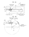
- FIG. 6 illustrates the wavelength tunability of the wavelength tunable light source 500 of FIG. 5.
- the wavelength tunable light source 500 illustrated in FIGS. 6A and 6B is structured to satisfy the Littrow condition defined by Equation 3.
- the wavelength tunable light source 500 illustrated in FIG. 6A includes the SOA 510, the beam steering unit 520, and the concave diffraction grating 530 integrated on a single semiconductor substrate 501 formed of, for example, Indium Phosphide(InP) or Galium Arsenide(GaAs) .
- the SOA 510 may be a semiconductor laser diode, and a current I SOA may be supplied to the SOA 510.
- the beam steering unit 520 includes two electrodes, and electrical signals, for example, the currents I BS1 and I BS2 , may be transmitted to the two electrodes.
- the concave diffraction grating 530 is disposed in a side region of the semiconductor substrate 501.
- the structure of the concave diffraction grating 530 is not limited to a particular structure.
- the concave diffraction grating 530 structured as a Rowland circle 540 is presented for the current description.
- a concave diffraction grating circle 535 based on the Rowland circle 540 is illustrated in FIG. 6B.
- the concave diffraction grating circle 535 and the Rowland circle 540 meet at a point P, and a base line 610 extends from a center C of the concave diffraction grating circle 535 to the point P.
- a side of the Rowland circle 540 contacts the beam steering unit 520.
- the wavelength tunable light source 500 can operate as a laser diode.
- a beam 620 emitted from the SOA 510 toward the concave diffraction grating 530 passes through the beam steering unit 520 and is incident on the concave diffraction grating 530 at the point P.
- a particular single wavelength optical signal is fed back to the SOA at an angle equal to an incident angle ⁇ according to the diffraction characteristics of the concave diffraction grating 530. Consequently, a beam 600 having the particular wavelength is output as indicated by an arrow Pout1.
- the wavelength of the output beam 600 is determined by the Littrow diffraction grating equation (Equation 3).
- the incident angle ⁇ indicates an angle formed by the base line 610 and the path of the incident beam 620 as illustrated in FIGS. 6A and 6B.
- the beam steering unit 520 includes two electrodes and steers a beam by adjusting the difference between the currents I BS1 and I BS2 supplied to the two electrodes. Accordingly, the incident angle ⁇ of the beam 620 whose path can been changed.
- the wavelength of the diffracted beam 620 is changed according to Equation 3 based on the change in the incident angle ⁇ of the beam 620.
- the beam steering unit-integrated wavelength tunable light source 500 can perform fast and stable wavelength tuning through electrical adjustment. Since all elements are integrated in a single substrate, the size of the wavelength tunable light source is small. In addition, since current is injected into a region around the beam path, optical loss due to wavelength tuning is small and optical output is hardly varied.
- the location at which the beam 620 is steered is on the Rowland circle 540, and the width of the beam steering unit 520 is large. Therefore, the two electrodes included in the beam steering unit 520 are asymmetrical with respect to each other, which distorts the shape of the beam 620 steered by the beam steering unit 520 and makes it impossible to place the beam 620 precisely on the Rowland circle 540. Consequently, the coupling characteristics of a beam spread from the Rowland circle 540 to the concave diffraction grating 530 and a beam fed back from the concave diffraction grating 530 to the Rowland circle 540 are low, which results in low optical output.
- the optical deflector-integrated wavelength tunable light source including the Roland-circle-based diffraction grating described with reference to FIGS. 3 and 4 has high optical output
- the optical deflector 330 is placed on the beam path, optical loss is increased during wavelength tuning, which results in variations in the optical output.
- the beam steering unit-integrated wavelength tunable light source 500 including the Roland-circle-based diffraction grating 530 described with reference to FIGS. 5 and 6 has an optical output with low variation since the two electrodes included in the beam steering unit 520 are disposed near the beam path.
- the two electrodes are asymmetrical with respect to each other, the coupling efficiency is reduced and the optical output is low.
- optical deflector-integrated wavelength tunable light sources including the Roland-circle-based diffraction grating are integrated in a single substrate formed of Indium Phosphide(InP) or Galium Arsenide(GaAs).
- the concave diffraction grating 340 is formed of Indium Phosphide(InP) or Galium Arsenide(GaAs), the concave diffraction grating 340 cannot be precisely patterned due to uneven etching characteristics of the Indium Phosphide(InP) or Galium Arsenide(GaAs).
- the concave diffraction grating 340 formed of silicon or polymer which has uniform etching characteristics and can be precisely patterned, and the SOA 310 formed of the Indium Phosphide(InP) or Galium Arsenide(GaAs) may be desirable.
- FIG. 7 is a schematic diagram of a beam steering unit-integrated wavelength tunable light source 700 including a concave diffraction grating 730 which provides a straight beam track according to an embodiment of the present invention.
- the wavelength tunable light source 700 includes an SOA 710, a beam steering unit 720, and the concave diffraction grating 730 integrated on a single substrate formed of Indium Phosphide(InP) or Galium Arsenide(GaAs).
- the SOA 710 may be a semiconductor laser diode, and a current I SOA may be supplied to the SOA 710.
- the beam steering unit 720 includes two electrodes, and currents I BS1 and I BS2 may be transmitted to the two electrodes.
- the concave diffraction grating 730 is disposed in a side region of the semiconductor substrate 701.
- the structure of the concave diffraction grating 730 can be similar to the concave diffraction grating 530 illustrated in FIG. 5.
- the structure of the concave diffraction grating 730 is not limited to a particular structure. That is, the concave diffraction grating 730 according to the present embodiment is not a Rowland circle-based diffraction grating. Instead, the concave diffraction grating 730 is structured such that the track of points to which a beam is diffracted by the concave diffraction grating 730 is straight.
- the two electrodes included in the beam steering unit 720 are formed symmetrical to each other, and positions to which the beam is diffracted are moved along the straight line according to the difference between the currents supplied to the two electrodes.
- FIG. 8 illustrates the concave diffraction grating 730 of FIG. 7 which makes the track of a wavelength tunable beam straight.
- the length of a line S N between the point P N and a point B, the line forming a side of a triangle formed by the points A, B and P N may be defined by Equation 7 based on the second law of cosines.
- Equation 7 defines the relationship between S N and (R N , ⁇ N ).
- the second term in the root in the second line of Equation 7 can be ignored since it is very small relative to the other terms in the root.
- the third line of Equation 7 is a binominal approximation obtained by Taylor-expanding the root.
- Equation 7 the second line is obtained using Equation 7, thus providing the relationship between S N+1 and (R N , ⁇ N )).
- Equation 9 indicates the relationship between S N+1 and (R N+1 , ⁇ N+1 ). By using Equation 6, the relationship between S N+1 and (R N , ⁇ N+1 ) can be obtained.
- the third line of Equation 9 is obtained using the binominal approximation of Equation 7 and the fourth line of Equation 9 is obtained using Equation 6.
- R N+1 , S N , S N+1 , and ⁇ N+1 can be obtained using Equations 6 through 9, and this can be performed for all values of N through reiteration.
- the variation in wavelength can be defined by a first line of Equation 10 based on the second line of Equation 8 and the fourth line of Equation 9.
- sin ⁇ N and sin ⁇ N+1 can be respectively approximated by ⁇ N and ⁇ N+1 since the angles are relatively small (maximum 15 degrees)
- g denotes a diffraction grating spacing (a design variable equal to the distance between P N and P N+1 ).
- Equation 11 the variation in the wavelength linearly increases according to structure variables as the diffraction grating d increases.
- Equations 6 through 11 described above have been presented to easily describe the present invention. However, since approximations are not used when the present invention is actually designed, more complicated equations may be required.
- the diffraction grating spacing g may be artificially changed to make the relationship between d and the variation in the wavelength ⁇ ⁇ linear.
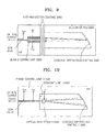
- FIG. 9 is a schematic diagram of a wavelength tunable light source with a hybrid integration of a concave diffraction grating 940, which provides a straight beam track and is formed of silicon or polymer, and an SOA 910 and a beam steering unit 920, which are formed of Indium Phosphide(InP) or Galium Arsenide(GaAs), according to an embodiment of the present invention.
- a concave diffraction grating 940 which provides a straight beam track and is formed of silicon or polymer
- SOA 910 and a beam steering unit 920 which are formed of Indium Phosphide(InP) or Galium Arsenide(GaAs), according to an embodiment of the present invention.
- the concave diffraction grating 940 When the concave diffraction grating 940 is formed of Indium Phosphide(InP) or Galium Arsenide(GaAs), the concave diffraction grating 940 cannot be precisely patterned due to uneven etching characteristics of the Indium Phosphide(InP) or Galium Arsenide(GaAs), which results in high optical loss.
- the concave diffraction grating 940 formed of silicon or polymer which has even etching characteristics and can be precisely patterned, and the SOA 910 formed of Indium Phosphide(InP) or Galium Arsenide(GaAs) may be integrated in a hybrid manner.
- the left end of the waveguide is on the Rowland circle 350 or 540. Therefore, the hybrid integration is virtually impossible. However, in the wavelength tunable light source according to an embodiment of the present invention, since the track of a beam diffracted by the concave diffraction grating 730 forms a straight line, the hybrid integration is possible.
- Indium Phosphide(InP) or Galium Arsenide(GaAs) can be easily and evenly scribed along a line perpendicular to an optical output direction, and the reflection of the optical output is approximately thirty percent.
- anti-reflection coating 930 is required for a cross section of the Indium Phosphide(InP) or Galium Arsenide(GaAs).
- the anti-reflection coating 930 may be formed on the concave diffraction grating 940. Impedance matching oil may also be added to obtain better optical coupling characteristics.
- FIG. 10 is a schematic diagram of an optical deflector-integrated wavelength tunable light source including a concave diffraction grating 1030 which provides a straight beam track according to an embodiment of the present invention.
- the wavelength tunable light source of FIG. 10 may include an optical deflector 1020 integrated therein.
- Rowland circle-based diffraction gratings have aberrations. Such aberrations are removed by adjusting diffraction grating spacing.
- the diffraction grating spacing can be adjusted when the diffraction grating 730, 940 or 1030 is designed. Further, aberrations can be completely removed, and it is relatively easy to design and manufacture the linear pattern of the diffraction grating 730, 940 or 1030.
- FIG. 11 is a schematic diagram of a beam steering unit-integrated wavelength tunable light source 1100 including a concave diffraction grating 1130 which satisfies the Littman condition defined by Equation 12 and provides a straight beam track according to an embodiment of the present invention.
- the wavelength tunable light source 1100 (wavelength tunable laser) of FIG. 11 is structured to satisfy the Littman condition defined by Equation 12.
- An angle at which a beam is incident on the concave diffraction grating 1130 is changed as the position at which the beam is incident on the concave diffraction grating 1130 varies when current is injected into the beam steering unit 1120. In this way, wavelength tuning is performed.
- the incident angle ⁇ indicates an angle formed by a base line 1160, which extends from the center of a concave diffraction grating circle to a point P, and the path of an incident beam 1180.
- the diffraction angle ⁇ is an angle formed by the base line 1160 and a beam 1190 reflected toward second SOAs or optical waveguides 1140.
- the wavelength tunable light source 1100 of FIG. 11 includes the concave diffraction grating 1130 structured such that wavelength tunable beams are collected along a straight line 1150.
- the beam 1180 emitted from a first SOA 1110 passes through the beam steering unit 1120 and is incident on the concave diffraction grating 1130.
- portions 1190 having particular wavelengths are fed back to the second SOAs or optical waveguides 1140 at different diffraction angles ⁇ according to the diffraction characteristics of the concave diffraction grating 1130. Consequently, beams 1170,...,1170-n-1 having particular wavelengths are output as indicated by arrows Pout2,...,Poutn.
- the wavelength tunable light source 1100 functions as a laser diode due to resonance that occurs since the left end of the first SOA 1110 and the left ends of the second SOAs 1140 are reflective surfaces.
- the wavelength tunable light source 1100 additionally includes the optical waveguides or second SOAs 1140 for guiding or amplifying the beam 1190 diffracted by the concave diffraction grating 1130 at the diffraction angle ⁇
- the wavelength tunable light source 1100 operates more stably and has more possible designs than the wavelength tunable light source 700 of FIG. 7.
- the wavelength tunable light source 700 of FIG. 7 includes one optical output terminal
- the wavelength tunable light source 1100 of FIG. 11 includes two or more optical output terminals since optical outputs can be obtained from the left end of the first SOA 1110 and the optical waveguides or the second SOAs 1140.
- the waveguides or second SOAs 1140 included in the wavelength tunable light source 1100 resonate light and output a beam having a number of wavelengths equal to the number of second SOAs or waveguides 1140.
- the wavelengths of the beams in the optical waveguides or second SOAs 1140 are changed by controlling the amount of current injected into the beam steering unit 1120.
- variable amount of wavelength can be increased by the number of optical wavelengths or second SOAs 1140.
- FIG. 12 is a schematic diagram of a wavelength tunable light source with a hybrid integration of a concave diffraction grating, which is formed of silicon or polymer, and an SOA and a beam steering unit, which are formed of Indium Phosphide(InP) or Galium Arsenide(GaAs), according to an embodiment of the present invention.
- the concave diffraction grating When the concave diffraction grating is formed of Indium Phosphide(InP) or Galium Arsenide(GaAs), the concave diffraction grating cannot be precisely patterned due to uneven etching characteristics of the Indium Phosphide(InP) or Galium Arsenide(GaAs), which results in high optical loss.
- the concave diffraction grating formed of silicon or polymer which has even etching characteristics and can be precisely patterned, and the SOA formed of the Indium Phosphide(InP) or Galium Arsenide(GaAs) may be integrated in a hybrid manner.
- Indium Phosphide(InP) or Galium Arsenide(GaAs) can be easily and evenly scribed along a line perpendicular to an optical output direction, and the reflection of the optical output is approximately thirty percent.
- anti-reflection coating 1230 is required for a cross section of the Indium Phosphide(InP) or Galium Arsenide(GaAs).
- the anti-reflection coating 1230 may be formed on the concave diffraction grating. Impedance matching oil may also be added to obtain better optical coupling characteristics.
- FIG. 13 is a schematic diagram of an optical deflector-integrated wavelength tunable light source including a concave diffraction grating 1330 which satisfies the Littman condition and provides a straight beam track according to an embodiment of the present invention.
- the wavelength tunable light source of FIG. 13 is identical to the wavelength tunable light source 1100 of FIG. 11 except that the wavelength tunable light source of FIG. 13 deflects a beam using an optical deflector 1320 instead of a beam steering unit.
- FIG. 14 is a flowchart illustrating an operating principle of the wavelength tunable light source 700 of FIG. 7. Referring to FIG. 14, an optical signal having a predetermined wavelength band is output from the SOA 710 (operation S1400).
- An optical deflector of the beam steering unit 720 deflects an output path of the optical signal having the predetermined wavelength band according to the amount of current supplied to the optical deflector (operation S1410).
- the concave diffraction grating 730 having a predetermined grating spacing reflects and diffracts the optical signal having the predetermined wavelength band such that a single wavelength optical signal in the predetermined wavelength band has constructive interference (operation S1420).
- the constructively-interfered optical signal is fed back to the SOA 710 (operation S1430).
- the optical signal fed back to the SOA 710 is amplified and then output (operation S1440). Lasing occurs when a gain of the amplified optical signal is identical to optical loss within the SOA 710.
- FIG. 15 is a flowchart illustrating an operating principle of the wavelength tunable light source 1100 of FIG. 11. Referring to FIG. 15, an optical signal having a predetermined wavelength band is output from the first SOA 1110 (operation S1500).
- An optical deflector of the beam steering unit 1120 deflects an output path of the optical signal having the predetermined wavelength band according to the amount of current supplied to the optical deflector (operation S1510).
- the concave diffraction grating 1130 having a predetermined grating spacing reflects and diffracts the optical signal having the predetermined wavelength band such that constructive interference occurs at ends of the linear waveguides, which respectively correspond to different wavelengths in the predetermined wavelength band (operation S1520).
- the second SOAs 1140 respectively input at least one optical signal separated according to wavelength to the concave diffraction grating 1130 (operation S1530).
- the concave diffraction grating 1130 feeds the at least one the optical signal to the first SOA 1110, which then amplifies the at least one optical signal and outputs the amplified optical signal (operation S1540).
- a wavelength tunable light source includes an SOA, a beam steering unit, and a concave diffraction grating integrated therein.
- the concave diffraction grating diffracts a beam to points on a straight line.
- Two electrodes included in the beam steering unit are symmetrical to each other, and thus prevent beam distortion.
- the two electrodes enable a beam to be accurately placed on the straight track, the coupling characteristics of a beam spread to the concave diffraction grating and a beam fed back from the concave diffraction grating to a cross section of the SOA are excellent, and thus high optical output can be achieved.
- the concave diffraction grating can be formed of a material other than Indium Phosphide(InP) or Galium Arsenide(GaAs).
- the concave diffraction grating can be formed of a material (silicon or polymer) which has reliable reproduction characteristics, and then integrated with the SOA or the laser diode formed of the Indium Phosphide(lnP) or Galium Arsenide(GaAs) in a hybrid manner. Consequently, optical coupling loss between the two materials can be minimized, and the reliability of the wavelength tunable light source can be increased.
Landscapes
- Physics & Mathematics (AREA)
- Condensed Matter Physics & Semiconductors (AREA)
- General Physics & Mathematics (AREA)
- Electromagnetism (AREA)
- Optics & Photonics (AREA)
- Semiconductor Lasers (AREA)
- Optical Modulation, Optical Deflection, Nonlinear Optics, Optical Demodulation, Optical Logic Elements (AREA)
Applications Claiming Priority (2)
| Application Number | Priority Date | Filing Date | Title |
|---|---|---|---|
| KR20050121038 | 2005-12-09 | ||
| KR1020060012026A KR100701153B1 (ko) | 2005-12-09 | 2006-02-08 | 파장 가변 광원 소자 |
Publications (2)
| Publication Number | Publication Date |
|---|---|
| EP1796231A2 true EP1796231A2 (fr) | 2007-06-13 |
| EP1796231A3 EP1796231A3 (fr) | 2008-05-21 |
Family
ID=37847060
Family Applications (1)
| Application Number | Title | Priority Date | Filing Date |
|---|---|---|---|
| EP06125505A Withdrawn EP1796231A3 (fr) | 2005-12-09 | 2006-12-06 | Source de lumière à longueur d'onde accordable |
Country Status (3)
| Country | Link |
|---|---|
| US (1) | US20070133649A1 (fr) |
| EP (1) | EP1796231A3 (fr) |
| JP (1) | JP2007165890A (fr) |
Cited By (1)
| Publication number | Priority date | Publication date | Assignee | Title |
|---|---|---|---|---|
| EP2056141A1 (fr) * | 2007-11-01 | 2009-05-06 | Electronics and Telecommunications Research Institute | Routeur spatial sélectif de longueur d'onde |
Families Citing this family (5)
| Publication number | Priority date | Publication date | Assignee | Title |
|---|---|---|---|---|
| KR100759820B1 (ko) * | 2006-07-18 | 2007-09-18 | 한국전자통신연구원 | 긴 공동 단일모드 레이저 다이오드 |
| KR100817726B1 (ko) * | 2008-01-18 | 2008-03-31 | 주식회사 나노베이스 | 파장 가변 장치 및 그 방법 |
| CN101800393B (zh) * | 2010-04-09 | 2011-05-18 | 浙江大学 | 一种基于衍射光栅的集成化阵列波导激光器 |
| EP3029783B1 (fr) * | 2014-12-01 | 2020-03-04 | Huawei Technologies Co., Ltd. | Laser accordable à canaux multiples |
| KR102530560B1 (ko) * | 2016-08-26 | 2023-05-09 | 삼성전자주식회사 | 레이저빔 스티어링 소자 및 이를 포함하는 시스템 |
Family Cites Families (19)
| Publication number | Priority date | Publication date | Assignee | Title |
|---|---|---|---|---|
| GB2225482B (en) * | 1988-11-23 | 1992-10-14 | Stc Plc | Multichannel cavity laser |
| JPH02250384A (ja) * | 1989-03-24 | 1990-10-08 | Nippon Telegr & Teleph Corp <Ntt> | 波長可変半導体レーザ光源装置 |
| JPH05198893A (ja) * | 1991-09-30 | 1993-08-06 | Fuji Xerox Co Ltd | 波長多重レーザー発振器 |
| JP3191998B2 (ja) * | 1992-09-01 | 2001-07-23 | 富士ゼロックス株式会社 | 光通信用波長多重送受信器 |
| JP3023942B2 (ja) * | 1992-06-18 | 2000-03-21 | 日本電信電話株式会社 | 波長チュウニング型小型分光器 |
| US5351262A (en) * | 1992-09-10 | 1994-09-27 | Bell Communications Research, Inc. | Multi-stripe array grating integrated cavity laser |
| JPH0933960A (ja) * | 1995-07-14 | 1997-02-07 | Nec Corp | 半導体レーザ装置及びその駆動方法 |
| JP2947142B2 (ja) * | 1995-09-21 | 1999-09-13 | 日本電気株式会社 | 波長可変半導体レーザ |
| JP3602664B2 (ja) * | 1996-09-26 | 2004-12-15 | 財団法人電力中央研究所 | 波長可変レーザ光発生方法およびその装置 |
| JPH1168248A (ja) * | 1997-08-21 | 1999-03-09 | Ando Electric Co Ltd | 外部共振器型波長可変半導体レーザ光源 |
| JPH11186664A (ja) * | 1997-12-24 | 1999-07-09 | Tera Tec:Kk | 波長可変光源 |
| JP3004971B1 (ja) * | 1998-09-21 | 2000-01-31 | 日本電信電話株式会社 | アレイ導波路回折格子およびアレイ導波路回折格子を用いた光信号処理回路 |
| US6434299B1 (en) * | 1999-06-01 | 2002-08-13 | Lightchip, Inc. | Wavelength division multiplexing/demultiplexing devices having concave diffraction gratings |
| US6501782B1 (en) * | 1999-10-25 | 2002-12-31 | Aculight Corporation | Compact laser apparatus |
| JP2001177182A (ja) * | 1999-12-16 | 2001-06-29 | Fujitsu Ltd | 外部共振器型半導体レーザおよび光導波路装置 |
| US6678445B2 (en) * | 2000-12-04 | 2004-01-13 | Jds Uniphase Corporation | Dynamic gain flattening filter |
| AU2003287709A1 (en) * | 2002-11-13 | 2004-06-03 | Battelle Memorial Institute | Optical wavelength division mux/demux with integrated optical amplifier |
| KR100523080B1 (ko) * | 2003-10-15 | 2005-10-24 | 한국전자통신연구원 | 편향기 집적 동적 단일모드 레이저 다이오드를 이용한변조 장치 |
| KR100550141B1 (ko) * | 2004-08-09 | 2006-02-08 | 한국전자통신연구원 | 가변 광 편향기를 이용한 파장 가변형 외부 공진 레이저다이오드 |
-
2006
- 2006-12-05 US US11/634,277 patent/US20070133649A1/en not_active Abandoned
- 2006-12-06 EP EP06125505A patent/EP1796231A3/fr not_active Withdrawn
- 2006-12-11 JP JP2006332955A patent/JP2007165890A/ja active Pending
Non-Patent Citations (3)
| Title |
|---|
| "Continuous Tuning of an Electrically Tunable External-Cavity Semiconductor Laser", OPTICS LETTERS, vol. 25, no. 16, 15 August 2000 (2000-08-15), pages 165 - 1167 |
| KIM H.S., MONOLITHICALLY INTEGRATED GRATING CAVITY TUNABLE LASERS |
| KIM K. H., MONOLITICALLY INTEGRATED EXTERNAL CAVITY WAVELENGTH TUNABLE LASER USING BEAM STEERING CONTROLLER |
Cited By (1)
| Publication number | Priority date | Publication date | Assignee | Title |
|---|---|---|---|---|
| EP2056141A1 (fr) * | 2007-11-01 | 2009-05-06 | Electronics and Telecommunications Research Institute | Routeur spatial sélectif de longueur d'onde |
Also Published As
| Publication number | Publication date |
|---|---|
| US20070133649A1 (en) | 2007-06-14 |
| EP1796231A3 (fr) | 2008-05-21 |
| JP2007165890A (ja) | 2007-06-28 |
Similar Documents
| Publication | Publication Date | Title |
|---|---|---|
| JP4610569B2 (ja) | 光偏向器を備えた波長可変逆多重化器 | |
| US7738527B2 (en) | Wavelength switchable semiconductor laser using half-wave coupled active double-ring resonator | |
| CN104937791B (zh) | 激光装置、光调制装置以及光半导体元件 | |
| KR100916311B1 (ko) | 이중 결합 링 공진기를 이용한 파장 가변 레이저 다이오드 | |
| US4935930A (en) | Laser light source for generating beam collimated in at least one direction | |
| JP4954992B2 (ja) | 半導体光反射素子及び該半導体光反射素子を用いる半導体レーザ及び該半導体レーザを用いる光トランスポンダ | |
| US6822980B2 (en) | Tunable semiconductor laser with integrated wideband reflector | |
| US6697392B2 (en) | Single wavelength laser module | |
| US7949020B2 (en) | Semiconductor laser and optical integrated semiconductor device | |
| US20060140228A1 (en) | Semi-integrated designs with in-waveguide mirrors for external cavity tunable lasers | |
| JP2003289169A (ja) | 半導体レーザ装置 | |
| EP1796231A2 (fr) | Source de lumière à longueur d'onde accordable | |
| US7382817B2 (en) | V-coupled-cavity semiconductor laser | |
| JP2011086714A (ja) | 波長可変レーザ | |
| US7852897B2 (en) | Semiconductor laser optical integrated semiconductor device | |
| US20060140569A1 (en) | Planar waveguides with air thin films used as anti-reflective layers, beam splitters and mirrors | |
| JP5034572B2 (ja) | 光源装置 | |
| KR100701153B1 (ko) | 파장 가변 광원 소자 | |
| US20030103761A1 (en) | Folded light path for planar optical devices | |
| US20260081400A1 (en) | Multi-wavelength laser | |
| JP3989939B2 (ja) | 光増幅器、ビーム操縦器及び凹回折格子が集積された波長可変光源素子 | |
| JPS63305581A (ja) | 発振波長可変型半導体レ−ザ装置 | |
| KR100744548B1 (ko) | 광증폭기, 빔 조종기 및 오목 회절 격자가 집적된 파장가변 광원 소자 | |
| KR20130131559A (ko) | 파장 가변 광필터 및 광원 |
Legal Events
| Date | Code | Title | Description |
|---|---|---|---|
| PUAI | Public reference made under article 153(3) epc to a published international application that has entered the european phase |
Free format text: ORIGINAL CODE: 0009012 |
|
| AK | Designated contracting states |
Kind code of ref document: A2 Designated state(s): AT BE BG CH CY CZ DE DK EE ES FI FR GB GR HU IE IS IT LI LT LU LV MC NL PL PT RO SE SI SK TR |
|
| AX | Request for extension of the european patent |
Extension state: AL BA HR MK YU |
|
| RIN1 | Information on inventor provided before grant (corrected) |
Inventor name: OH, KWANG RYONG Inventor name: SIM, EUNDEOK Inventor name: KIM, JONGHOI Inventor name: KIM, KANG HO Inventor name: KWON, OH KEE |
|
| PUAL | Search report despatched |
Free format text: ORIGINAL CODE: 0009013 |
|
| AK | Designated contracting states |
Kind code of ref document: A3 Designated state(s): AT BE BG CH CY CZ DE DK EE ES FI FR GB GR HU IE IS IT LI LT LU LV MC NL PL PT RO SE SI SK TR |
|
| AX | Request for extension of the european patent |
Extension state: AL BA HR MK RS |
|
| RIC1 | Information provided on ipc code assigned before grant |
Ipc: G02B 6/34 20060101ALN20080411BHEP Ipc: H01S 5/40 20060101ALI20080411BHEP Ipc: H01S 5/14 20060101AFI20070322BHEP |
|
| 17P | Request for examination filed |
Effective date: 20080814 |
|
| 17Q | First examination report despatched |
Effective date: 20080919 |
|
| AKX | Designation fees paid |
Designated state(s): AT BE BG CH CY CZ DE DK EE ES FI FR GB GR HU IE IS IT LI LT LU LV MC NL PL PT RO SE SI SK TR |
|
| STAA | Information on the status of an ep patent application or granted ep patent |
Free format text: STATUS: THE APPLICATION IS DEEMED TO BE WITHDRAWN |
|
| 18D | Application deemed to be withdrawn |
Effective date: 20130702 |