EP1806961A1 - Absorbeur d'ondes electromagnetiques - Google Patents
Absorbeur d'ondes electromagnetiques Download PDFInfo
- Publication number
- EP1806961A1 EP1806961A1 EP05788222A EP05788222A EP1806961A1 EP 1806961 A1 EP1806961 A1 EP 1806961A1 EP 05788222 A EP05788222 A EP 05788222A EP 05788222 A EP05788222 A EP 05788222A EP 1806961 A1 EP1806961 A1 EP 1806961A1
- Authority
- EP
- European Patent Office
- Prior art keywords
- electromagnetic wave
- pattern
- wave absorber
- layer
- conductive
- Prior art date
- Legal status (The legal status is an assumption and is not a legal conclusion. Google has not performed a legal analysis and makes no representation as to the accuracy of the status listed.)
- Withdrawn
Links
- 239000006096 absorbing agent Substances 0.000 title claims abstract description 206
- 230000010287 polarization Effects 0.000 claims abstract description 90
- 239000000463 material Substances 0.000 claims description 70
- 238000006073 displacement reaction Methods 0.000 claims description 24
- 238000000926 separation method Methods 0.000 claims description 24
- 239000011800 void material Substances 0.000 claims description 18
- 238000000034 method Methods 0.000 claims description 14
- 230000035699 permeability Effects 0.000 claims description 14
- 229910000859 α-Fe Inorganic materials 0.000 claims description 14
- XEEYBQQBJWHFJM-UHFFFAOYSA-N Iron Chemical compound [Fe] XEEYBQQBJWHFJM-UHFFFAOYSA-N 0.000 claims description 11
- 230000002093 peripheral effect Effects 0.000 claims description 9
- 229920000620 organic polymer Polymers 0.000 claims description 6
- 229910000640 Fe alloy Inorganic materials 0.000 claims description 4
- 239000003989 dielectric material Substances 0.000 claims description 4
- 238000010030 laminating Methods 0.000 claims description 4
- 238000002156 mixing Methods 0.000 claims description 4
- 238000010521 absorption reaction Methods 0.000 abstract description 242
- 230000001747 exhibiting effect Effects 0.000 abstract 1
- 239000010410 layer Substances 0.000 description 273
- 239000003990 capacitor Substances 0.000 description 19
- 230000005684 electric field Effects 0.000 description 19
- 239000003063 flame retardant Substances 0.000 description 13
- 229910052751 metal Inorganic materials 0.000 description 12
- 239000002184 metal Substances 0.000 description 12
- 230000005540 biological transmission Effects 0.000 description 11
- 230000008901 benefit Effects 0.000 description 10
- 238000004088 simulation Methods 0.000 description 10
- OKTJSMMVPCPJKN-UHFFFAOYSA-N Carbon Chemical compound [C] OKTJSMMVPCPJKN-UHFFFAOYSA-N 0.000 description 9
- 229920005989 resin Polymers 0.000 description 9
- 239000011347 resin Substances 0.000 description 9
- 229920002799 BoPET Polymers 0.000 description 8
- VTYYLEPIZMXCLO-UHFFFAOYSA-L Calcium carbonate Chemical compound [Ca+2].[O-]C([O-])=O VTYYLEPIZMXCLO-UHFFFAOYSA-L 0.000 description 8
- 230000000694 effects Effects 0.000 description 8
- 230000006872 improvement Effects 0.000 description 8
- 239000000203 mixture Substances 0.000 description 8
- 239000012790 adhesive layer Substances 0.000 description 7
- 229910045601 alloy Inorganic materials 0.000 description 7
- 239000000956 alloy Substances 0.000 description 7
- 238000004891 communication Methods 0.000 description 7
- 239000004020 conductor Substances 0.000 description 7
- 229910002804 graphite Inorganic materials 0.000 description 7
- IJGRMHOSHXDMSA-UHFFFAOYSA-N Atomic nitrogen Chemical compound N#N IJGRMHOSHXDMSA-UHFFFAOYSA-N 0.000 description 6
- 238000005516 engineering process Methods 0.000 description 6
- 230000004907 flux Effects 0.000 description 6
- 239000010439 graphite Substances 0.000 description 6
- 238000003475 lamination Methods 0.000 description 6
- 239000006229 carbon black Substances 0.000 description 5
- DOIRQSBPFJWKBE-UHFFFAOYSA-N dibutyl phthalate Chemical compound CCCCOC(=O)C1=CC=CC=C1C(=O)OCCCC DOIRQSBPFJWKBE-UHFFFAOYSA-N 0.000 description 5
- 238000005259 measurement Methods 0.000 description 5
- 239000000123 paper Substances 0.000 description 5
- 239000011120 plywood Substances 0.000 description 5
- -1 polyethylene Polymers 0.000 description 5
- RNFJDJUURJAICM-UHFFFAOYSA-N 2,2,4,4,6,6-hexaphenoxy-1,3,5-triaza-2$l^{5},4$l^{5},6$l^{5}-triphosphacyclohexa-1,3,5-triene Chemical compound N=1P(OC=2C=CC=CC=2)(OC=2C=CC=CC=2)=NP(OC=2C=CC=CC=2)(OC=2C=CC=CC=2)=NP=1(OC=1C=CC=CC=1)OC1=CC=CC=C1 RNFJDJUURJAICM-UHFFFAOYSA-N 0.000 description 4
- PPBRXRYQALVLMV-UHFFFAOYSA-N Styrene Chemical compound C=CC1=CC=CC=C1 PPBRXRYQALVLMV-UHFFFAOYSA-N 0.000 description 4
- 229910000019 calcium carbonate Inorganic materials 0.000 description 4
- 239000000835 fiber Substances 0.000 description 4
- 239000000945 filler Substances 0.000 description 4
- 239000004800 polyvinyl chloride Substances 0.000 description 4
- 229920000915 polyvinyl chloride Polymers 0.000 description 4
- 239000000758 substrate Substances 0.000 description 4
- 229910052782 aluminium Inorganic materials 0.000 description 3
- XAGFODPZIPBFFR-UHFFFAOYSA-N aluminium Chemical compound [Al] XAGFODPZIPBFFR-UHFFFAOYSA-N 0.000 description 3
- 239000010426 asphalt Substances 0.000 description 3
- 230000002902 bimodal effect Effects 0.000 description 3
- 230000007547 defect Effects 0.000 description 3
- 238000009826 distribution Methods 0.000 description 3
- 239000004744 fabric Substances 0.000 description 3
- VNWKTOKETHGBQD-UHFFFAOYSA-N methane Chemical compound C VNWKTOKETHGBQD-UHFFFAOYSA-N 0.000 description 3
- 229910052757 nitrogen Inorganic materials 0.000 description 3
- 239000004745 nonwoven fabric Substances 0.000 description 3
- 238000005192 partition Methods 0.000 description 3
- 239000004014 plasticizer Substances 0.000 description 3
- 239000000843 powder Substances 0.000 description 3
- 239000002344 surface layer Substances 0.000 description 3
- 229920003002 synthetic resin Polymers 0.000 description 3
- 239000000057 synthetic resin Substances 0.000 description 3
- 229920001187 thermosetting polymer Polymers 0.000 description 3
- 239000011701 zinc Substances 0.000 description 3
- WKBOTKDWSSQWDR-UHFFFAOYSA-N Bromine atom Chemical compound [Br] WKBOTKDWSSQWDR-UHFFFAOYSA-N 0.000 description 2
- 229920000049 Carbon (fiber) Polymers 0.000 description 2
- RTZKZFJDLAIYFH-UHFFFAOYSA-N Diethyl ether Chemical compound CCOCC RTZKZFJDLAIYFH-UHFFFAOYSA-N 0.000 description 2
- 101001093748 Homo sapiens Phosphatidylinositol N-acetylglucosaminyltransferase subunit P Proteins 0.000 description 2
- PXHVJJICTQNCMI-UHFFFAOYSA-N Nickel Chemical compound [Ni] PXHVJJICTQNCMI-UHFFFAOYSA-N 0.000 description 2
- 229910001035 Soft ferrite Inorganic materials 0.000 description 2
- 229910000831 Steel Inorganic materials 0.000 description 2
- HCHKCACWOHOZIP-UHFFFAOYSA-N Zinc Chemical compound [Zn] HCHKCACWOHOZIP-UHFFFAOYSA-N 0.000 description 2
- XLOMVQKBTHCTTD-UHFFFAOYSA-N Zinc monoxide Chemical compound [Zn]=O XLOMVQKBTHCTTD-UHFFFAOYSA-N 0.000 description 2
- 239000000853 adhesive Substances 0.000 description 2
- 230000001070 adhesive effect Effects 0.000 description 2
- 239000004840 adhesive resin Substances 0.000 description 2
- 229920006223 adhesive resin Polymers 0.000 description 2
- 230000004075 alteration Effects 0.000 description 2
- 238000013459 approach Methods 0.000 description 2
- 230000002238 attenuated effect Effects 0.000 description 2
- 239000011230 binding agent Substances 0.000 description 2
- 150000001639 boron compounds Chemical class 0.000 description 2
- GDTBXPJZTBHREO-UHFFFAOYSA-N bromine Substances BrBr GDTBXPJZTBHREO-UHFFFAOYSA-N 0.000 description 2
- 229910052794 bromium Inorganic materials 0.000 description 2
- MTAZNLWOLGHBHU-UHFFFAOYSA-N butadiene-styrene rubber Chemical compound C=CC=C.C=CC1=CC=CC=C1 MTAZNLWOLGHBHU-UHFFFAOYSA-N 0.000 description 2
- 238000004364 calculation method Methods 0.000 description 2
- 239000004917 carbon fiber Substances 0.000 description 2
- 239000004568 cement Substances 0.000 description 2
- 229920006026 co-polymeric resin Polymers 0.000 description 2
- 229920001577 copolymer Polymers 0.000 description 2
- 230000007423 decrease Effects 0.000 description 2
- 238000013461 design Methods 0.000 description 2
- 230000006866 deterioration Effects 0.000 description 2
- 239000002270 dispersing agent Substances 0.000 description 2
- 230000007613 environmental effect Effects 0.000 description 2
- 239000003822 epoxy resin Substances 0.000 description 2
- 239000011888 foil Substances 0.000 description 2
- 239000003365 glass fiber Substances 0.000 description 2
- XLYOFNOQVPJJNP-UHFFFAOYSA-M hydroxide Chemical compound [OH-] XLYOFNOQVPJJNP-UHFFFAOYSA-M 0.000 description 2
- 229910052742 iron Inorganic materials 0.000 description 2
- 238000004898 kneading Methods 0.000 description 2
- 239000000696 magnetic material Substances 0.000 description 2
- 239000011159 matrix material Substances 0.000 description 2
- 239000012811 non-conductive material Substances 0.000 description 2
- 239000002245 particle Substances 0.000 description 2
- 150000003018 phosphorus compounds Chemical class 0.000 description 2
- 239000011505 plaster Substances 0.000 description 2
- BASFCYQUMIYNBI-UHFFFAOYSA-N platinum Chemical compound [Pt] BASFCYQUMIYNBI-UHFFFAOYSA-N 0.000 description 2
- 229920000647 polyepoxide Polymers 0.000 description 2
- 238000004321 preservation Methods 0.000 description 2
- 230000002265 prevention Effects 0.000 description 2
- 238000011160 research Methods 0.000 description 2
- 239000010959 steel Substances 0.000 description 2
- BIKXLKXABVUSMH-UHFFFAOYSA-N trizinc;diborate Chemical compound [Zn+2].[Zn+2].[Zn+2].[O-]B([O-])[O-].[O-]B([O-])[O-] BIKXLKXABVUSMH-UHFFFAOYSA-N 0.000 description 2
- 229910052725 zinc Inorganic materials 0.000 description 2
- CMQUQOHNANGDOR-UHFFFAOYSA-N 2,3-dibromo-4-(2,4-dibromo-5-hydroxyphenyl)phenol Chemical compound BrC1=C(Br)C(O)=CC=C1C1=CC(O)=C(Br)C=C1Br CMQUQOHNANGDOR-UHFFFAOYSA-N 0.000 description 1
- 229910021364 Al-Si alloy Inorganic materials 0.000 description 1
- 239000004709 Chlorinated polyethylene Substances 0.000 description 1
- VYZAMTAEIAYCRO-UHFFFAOYSA-N Chromium Chemical compound [Cr] VYZAMTAEIAYCRO-UHFFFAOYSA-N 0.000 description 1
- RYGMFSIKBFXOCR-UHFFFAOYSA-N Copper Chemical compound [Cu] RYGMFSIKBFXOCR-UHFFFAOYSA-N 0.000 description 1
- 229910019819 Cr—Si Inorganic materials 0.000 description 1
- 229910017758 Cu-Si Inorganic materials 0.000 description 1
- 229910017931 Cu—Si Inorganic materials 0.000 description 1
- 229910001047 Hard ferrite Inorganic materials 0.000 description 1
- 229910001030 Iron–nickel alloy Inorganic materials 0.000 description 1
- 239000004640 Melamine resin Substances 0.000 description 1
- 229920000877 Melamine resin Polymers 0.000 description 1
- 229910018605 Ni—Zn Inorganic materials 0.000 description 1
- 241000282320 Panthera leo Species 0.000 description 1
- 239000005062 Polybutadiene Substances 0.000 description 1
- 239000004698 Polyethylene Substances 0.000 description 1
- 239000004743 Polypropylene Substances 0.000 description 1
- BQCADISMDOOEFD-UHFFFAOYSA-N Silver Chemical compound [Ag] BQCADISMDOOEFD-UHFFFAOYSA-N 0.000 description 1
- 229910002796 Si–Al Inorganic materials 0.000 description 1
- 229910008423 Si—B Inorganic materials 0.000 description 1
- 229910008458 Si—Cr Inorganic materials 0.000 description 1
- GWEVSGVZZGPLCZ-UHFFFAOYSA-N Titan oxide Chemical compound O=[Ti]=O GWEVSGVZZGPLCZ-UHFFFAOYSA-N 0.000 description 1
- FMRLDPWIRHBCCC-UHFFFAOYSA-L Zinc carbonate Chemical compound [Zn+2].[O-]C([O-])=O FMRLDPWIRHBCCC-UHFFFAOYSA-L 0.000 description 1
- MUBKMWFYVHYZAI-UHFFFAOYSA-N [Al].[Cu].[Zn] Chemical compound [Al].[Cu].[Zn] MUBKMWFYVHYZAI-UHFFFAOYSA-N 0.000 description 1
- 239000002253 acid Substances 0.000 description 1
- 239000000654 additive Substances 0.000 description 1
- 230000000996 additive effect Effects 0.000 description 1
- 230000002411 adverse Effects 0.000 description 1
- WNROFYMDJYEPJX-UHFFFAOYSA-K aluminium hydroxide Chemical compound [OH-].[OH-].[OH-].[Al+3] WNROFYMDJYEPJX-UHFFFAOYSA-K 0.000 description 1
- SWLVFNYSXGMGBS-UHFFFAOYSA-N ammonium bromide Chemical compound [NH4+].[Br-] SWLVFNYSXGMGBS-UHFFFAOYSA-N 0.000 description 1
- 229940077484 ammonium bromide Drugs 0.000 description 1
- 230000003712 anti-aging effect Effects 0.000 description 1
- 230000015572 biosynthetic process Effects 0.000 description 1
- 239000006231 channel black Substances 0.000 description 1
- 238000006243 chemical reaction Methods 0.000 description 1
- 239000003795 chemical substances by application Substances 0.000 description 1
- 229910052804 chromium Inorganic materials 0.000 description 1
- 239000011651 chromium Substances 0.000 description 1
- 239000004927 clay Substances 0.000 description 1
- 238000005094 computer simulation Methods 0.000 description 1
- 239000000470 constituent Substances 0.000 description 1
- 229910052802 copper Inorganic materials 0.000 description 1
- 239000010949 copper Substances 0.000 description 1
- WCCJDBZJUYKDBF-UHFFFAOYSA-N copper silicon Chemical compound [Si].[Cu] WCCJDBZJUYKDBF-UHFFFAOYSA-N 0.000 description 1
- 230000008878 coupling Effects 0.000 description 1
- 238000010168 coupling process Methods 0.000 description 1
- 238000005859 coupling reaction Methods 0.000 description 1
- 238000005520 cutting process Methods 0.000 description 1
- 230000001419 dependent effect Effects 0.000 description 1
- 238000007599 discharging Methods 0.000 description 1
- 229920001971 elastomer Polymers 0.000 description 1
- 238000005530 etching Methods 0.000 description 1
- 239000006232 furnace black Substances 0.000 description 1
- 239000011521 glass Substances 0.000 description 1
- PCHJSUWPFVWCPO-UHFFFAOYSA-N gold Chemical compound [Au] PCHJSUWPFVWCPO-UHFFFAOYSA-N 0.000 description 1
- 229910052737 gold Inorganic materials 0.000 description 1
- 239000010931 gold Substances 0.000 description 1
- 230000005484 gravity Effects 0.000 description 1
- UPGZYVOGZSAYHA-UHFFFAOYSA-N guanidine;1,3,5-triazine-2,4,6-triamine Chemical class NC(N)=N.NC1=NC(N)=NC(N)=N1 UPGZYVOGZSAYHA-UHFFFAOYSA-N 0.000 description 1
- CAYGQBVSOZLICD-UHFFFAOYSA-N hexabromobenzene Chemical compound BrC1=C(Br)C(Br)=C(Br)C(Br)=C1Br CAYGQBVSOZLICD-UHFFFAOYSA-N 0.000 description 1
- 230000005764 inhibitory process Effects 0.000 description 1
- 239000011256 inorganic filler Substances 0.000 description 1
- 229910003475 inorganic filler Inorganic materials 0.000 description 1
- 239000011133 lead Substances 0.000 description 1
- 239000011777 magnesium Substances 0.000 description 1
- VTHJTEIRLNZDEV-UHFFFAOYSA-L magnesium dihydroxide Chemical compound [OH-].[OH-].[Mg+2] VTHJTEIRLNZDEV-UHFFFAOYSA-L 0.000 description 1
- 239000000347 magnesium hydroxide Substances 0.000 description 1
- 229910001862 magnesium hydroxide Inorganic materials 0.000 description 1
- 230000007257 malfunction Effects 0.000 description 1
- 230000007246 mechanism Effects 0.000 description 1
- ZQKXQUJXLSSJCH-UHFFFAOYSA-N melamine cyanurate Chemical compound NC1=NC(N)=NC(N)=N1.O=C1NC(=O)NC(=O)N1 ZQKXQUJXLSSJCH-UHFFFAOYSA-N 0.000 description 1
- 150000007974 melamines Chemical class 0.000 description 1
- 150000002736 metal compounds Chemical class 0.000 description 1
- 229910044991 metal oxide Inorganic materials 0.000 description 1
- 150000004706 metal oxides Chemical class 0.000 description 1
- 229910052759 nickel Inorganic materials 0.000 description 1
- 239000003973 paint Substances 0.000 description 1
- 238000009304 pastoral farming Methods 0.000 description 1
- 229910000889 permalloy Inorganic materials 0.000 description 1
- 239000005011 phenolic resin Substances 0.000 description 1
- 150000003014 phosphoric acid esters Chemical class 0.000 description 1
- 229910052698 phosphorus Inorganic materials 0.000 description 1
- 229910052697 platinum Inorganic materials 0.000 description 1
- 229920002857 polybutadiene Polymers 0.000 description 1
- 229920000573 polyethylene Polymers 0.000 description 1
- 229920000098 polyolefin Polymers 0.000 description 1
- 229920001155 polypropylene Polymers 0.000 description 1
- 229920002635 polyurethane Polymers 0.000 description 1
- 239000004814 polyurethane Substances 0.000 description 1
- 239000011118 polyvinyl acetate Substances 0.000 description 1
- 229920002689 polyvinyl acetate Polymers 0.000 description 1
- 239000011241 protective layer Substances 0.000 description 1
- 239000005060 rubber Substances 0.000 description 1
- 239000004576 sand Substances 0.000 description 1
- 229910000702 sendust Inorganic materials 0.000 description 1
- 238000004904 shortening Methods 0.000 description 1
- 229910052709 silver Inorganic materials 0.000 description 1
- 239000004332 silver Substances 0.000 description 1
- 239000002356 single layer Substances 0.000 description 1
- 239000002689 soil Substances 0.000 description 1
- 239000010935 stainless steel Substances 0.000 description 1
- 229910001220 stainless steel Inorganic materials 0.000 description 1
- 229920003051 synthetic elastomer Polymers 0.000 description 1
- 239000005061 synthetic rubber Substances 0.000 description 1
- 238000012360 testing method Methods 0.000 description 1
- 229920001169 thermoplastic Polymers 0.000 description 1
- 229920002725 thermoplastic elastomer Polymers 0.000 description 1
- 239000004416 thermosoftening plastic Substances 0.000 description 1
- OGIDPMRJRNCKJF-UHFFFAOYSA-N titanium oxide Inorganic materials [Ti]=O OGIDPMRJRNCKJF-UHFFFAOYSA-N 0.000 description 1
- JUWGUJSXVOBPHP-UHFFFAOYSA-B titanium(4+);tetraphosphate Chemical compound [Ti+4].[Ti+4].[Ti+4].[O-]P([O-])([O-])=O.[O-]P([O-])([O-])=O.[O-]P([O-])([O-])=O.[O-]P([O-])([O-])=O JUWGUJSXVOBPHP-UHFFFAOYSA-B 0.000 description 1
- 150000003918 triazines Chemical class 0.000 description 1
- WFKWXMTUELFFGS-UHFFFAOYSA-N tungsten Chemical compound [W] WFKWXMTUELFFGS-UHFFFAOYSA-N 0.000 description 1
- 229910052721 tungsten Inorganic materials 0.000 description 1
- 239000010937 tungsten Substances 0.000 description 1
- 239000002023 wood Substances 0.000 description 1
- 239000011667 zinc carbonate Substances 0.000 description 1
- 229910000010 zinc carbonate Inorganic materials 0.000 description 1
- 235000004416 zinc carbonate Nutrition 0.000 description 1
- 239000011787 zinc oxide Substances 0.000 description 1
Images






Classifications
-
- H—ELECTRICITY
- H05—ELECTRIC TECHNIQUES NOT OTHERWISE PROVIDED FOR
- H05K—PRINTED CIRCUITS; CASINGS OR CONSTRUCTIONAL DETAILS OF ELECTRIC APPARATUS; MANUFACTURE OF ASSEMBLAGES OF ELECTRICAL COMPONENTS
- H05K9/00—Screening of apparatus or components against electric or magnetic fields
- H05K9/0073—Shielding materials
- H05K9/0081—Electromagnetic shielding materials, e.g. EMI, RFI shielding
- H05K9/0088—Electromagnetic shielding materials, e.g. EMI, RFI shielding comprising a plurality of shielding layers; combining different shielding material structure
-
- H—ELECTRICITY
- H01—ELECTRIC ELEMENTS
- H01Q—ANTENNAS, i.e. RADIO AERIALS
- H01Q15/00—Devices for reflection, refraction, diffraction or polarisation of waves radiated from an antenna, e.g. quasi-optical devices
- H01Q15/0006—Devices acting selectively as reflecting surface, as diffracting or as refracting device, e.g. frequency filtering or angular spatial filtering devices
- H01Q15/0013—Devices acting selectively as reflecting surface, as diffracting or as refracting device, e.g. frequency filtering or angular spatial filtering devices said selective devices working as frequency-selective reflecting surfaces, e.g. FSS, dichroic plates, surfaces being partly transmissive and reflective
-
- H—ELECTRICITY
- H01—ELECTRIC ELEMENTS
- H01Q—ANTENNAS, i.e. RADIO AERIALS
- H01Q17/00—Devices for absorbing waves radiated from an antenna; Combinations of such devices with active antenna elements or systems
-
- H—ELECTRICITY
- H01—ELECTRIC ELEMENTS
- H01Q—ANTENNAS, i.e. RADIO AERIALS
- H01Q17/00—Devices for absorbing waves radiated from an antenna; Combinations of such devices with active antenna elements or systems
- H01Q17/007—Devices for absorbing waves radiated from an antenna; Combinations of such devices with active antenna elements or systems with means for controlling the absorption
Definitions
- the present invention relates to an electromagnetic wave absorber that catches an electromagnetic wave and absorbs it.
- a wireless LAN that uses microwaves is utilized and thereby a communication system more flexible and higher in the mobility is set up.
- FWA Fixed Wireless Access
- a communication service that communicates by wireless between a wide network system or an exchange network called FWA (Fixed Wireless Access) and communication apparatus that a user operates has started. That is, a wireless communication system is being utilized more and more familiarly.
- a short distance wireless technology called Bluetooth representative of a WPAN (Wireless Personal Area Network) is utilized as an alternative technology of a wire/cable technology.
- a communication system that uses a portable telephone that can verbally communicate due to a wireless LAN called a VoWLAN (Voice over Wireless Local Area Network) as well is expected to prevail.
- pattern electromagnetic wave absorber provided with a pattern layer having a conductive pattern (hereinafter, in some cases, simply referred to as "pattern”) is in use.
- the pattern electromagnetic wave absorber is disclosed in, for instance, Japanese Patent No. 3076473 (Japanese Unexamined Patent Publication JP-A 6-244583 (1994 )), Japanese Patent No. 3209456 (Japanese Unexamined Patent Publication JP-A 6-140787 (1994 )), Japanese Unexamined Patent Publications JP-A 11-204984 (1999 ) and JP-A 2002-246786 .
- JP-A 2002-246786 an electromagnetic wave absorber having a pattern layer excellent in the grazing incidence characteristics is disclosed.
- JP-A 11-204984 there is a description of a plurality of resonant frequency-selective electromagnetic wave shielding planar bodies and this relates to an electromagnetic wave absorber having a pattern layer having a bimodal characteristics.
- Pattern shapes used in the electromagnetic wave absorbers disclosed in the respective patent literatures are polygonal or circular and linear or planar shapes. There is found no literature that studies of an influence of a polarized wave of electromagnetic wave on the electromagnetic wave absorption characteristics.
- a pattern electromagnetic wave absorber works as a receiving antenna corresponding to an electromagnetic wave of a frequency of which pattern is absorbed to capture the electromagnetic wave and the captured electromagnetic wave is interfered by the pattern and a loss layer so as to attenuate or cancel out the electromagnetic wave to make a reflected wave smaller.
- Such a pattern electromagnetic wave absorber realizes a thin electromagnetic wave absorber that is tuned so as to resonate with an electromagnetic wave of a frequency to be absorbed.
- a dimension of a pattern is appropriately set so that a reflection amount of an electromagnetic wave of a frequency to be absorbed may be smaller.
- the polarization dependency of the pattern is large, it becomes difficult to make correspond to an electromagnetic wave of a frequency to be absorbed. That is, there is a problem in that, owing to a shape of a pattern, depending on a TE wave, TM wave, an electromagnetic wave entering from an arbitrary angle therebetween or a circularly polarized wave, the electromagnetic wave absorption characteristics, in particular, an absorption frequency varies, accordingly a problem in that the electromagnetic wave absorption characteristics have the polarization dependency.
- the pattern electromagnetic wave absorber involving parameters including a shape, number and arrangement of patterns, a dimension of a loss layer and material constants ( ⁇ ', ⁇ ", ⁇ ', ⁇ "), creates the optimum state and thereby realizes a high performance thin electromagnetic wave absorber, the optimum design of the absorption characteristics to a normally entering electromagnetic wave is established; however, depending on an incident angle of the electromagnetic wave or the polarization, the resonant state is readily affected to vary a resonant frequency.
- An object of the invention is to provide an electromagnetic wave absorber that has high peak value of absorption amount of an electromagnetic wave or is capable of absorbing electromagnetic waves of a plurality of frequencies, and is small in displacement between frequencies where peaks of absorption amount are reached, which displacement is caused by difference of polarization directions of electromagnetic waves.
- the invention provides an electromagnetic wave absorber comprising:
- a dimension of a portion that is formed in curve in the corner portion is determined at a small dimension within the range of dimension that can suppress displacement of frequency of electromagnetic wave which can be absorbed due to the difference of the polarization direction.
- the conductive pattern is a planar pattern.
- conductive patterns different in outer peripheral length are combined to form.
- conductive patterns different in curvature radius at corner portions are combined to form.
- a separation between two adjacent conductive patterns is different depending on a position.
- the conductive pattern has a single or plurality of void portions and the void portions resonate with an electromagnetic wave of a frequency to be absorbed.
- the loss layer includes:
- the electromagnetic wave absorbing layer includes as a magnetic loss material at least one selected from a group consisting of ferrite, iron alloy and iron powder at a blending ratio of 1 parts by weight or more and 1500 parts by weight or less to 100 parts by weight of an organic polymer.
- a real part ⁇ ' of the complex specific permittivity of the dielectric layer is in the range of 1 or more and 50 or less.
- the electromagnetic wave absorbing layer and the dielectric layer are 10 6 ⁇ /square or more in the surface resistivity.
- the electromagnetic wave absorbing layer or the dielectric layer is obtained by laminating a plurality of layers.
- the electromagnetic wave absorber is an electromagnetic wave absorber for absorbing an electromagnetic wave of 2. 4-GHz band, and a total thickness of the electromagnetic wave absorber is 4 mm or less.
- the electromagnetic wave absorber is an electromagnetic wave absorber for absorbing an electromagnetic wave of 900-MHz band, and a total thickness of the electromagnetic wave absorber is 10 mm or less.
- a conductive reflective layer is laminated on a side opposite to the pattern layer with respective to the loss layer.
- the electromagnetic wave absorber is flame resistant and nonflammable.
- the invention provides an electromagnetic wave absorbing method that uses any one of the electromagnetic wave absorbers mentioned above.
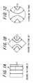
- Fig. 1 is a front view of a pattern P showing an influence that a direction of the pattern P affects on an electric field generated in the pattern P when in the pattern P an electromagnetic wave that is a TE wave is received.
- Fig. 1(1) shows how an electric field is generated when a square pattern P is placed in an opposite positional relationship in a direction of an electric field in an electromagnetic wave (hereinafter, in some cases, referred to as "polarization direction")
- Fig. 1(2) shows how an electric field is generated when a pattern P is displaced by 45° from the positional relationship of Fig. 1
- Fig. 1(3) shows how an electric field is generated in a case of a circular pattern P.
- Fig. 1(1) is a positional relationship of a square pattern P having sides in parallel with or vertical to a direction of an electric field of an electromagnetic wave.
- the positional relationship in Fig. 1(2) is a positional relationship where a square conductive pattern P is displaced by 45° from a position of Fig. 1(1).
- the square means a quadrangle of which four inner angles are right angles.
- the respective patterns P in Fig. 1 are conductive patterns.
- a direction E of an electric field generated in the pattern P is different depending on a shape of the pattern P, and, in the case of the square pattern P, is different as well depending on the positional relationship of the pattern P to the polarization direction of an electromagnetic wave.
- a direction E of an electric field generated in the pattern P is a linear direction in parallel with one side.
- a direction E of an electric field generated in the pattern P becomes substantially hyperbolic.
- a pattern that is used to receive an electromagnetic wave there are conductive patterns such as a circular pattern where irrespective of the polarization direction of an electromagnetic wave a receiving state is constant and a square pattern where depending on the polarization direction of an electromagnetic wave a receiving state is varied.
- conductive patterns such as a circular pattern where irrespective of the polarization direction of an electromagnetic wave a receiving state is constant and a square pattern where depending on the polarization direction of an electromagnetic wave a receiving state is varied.
- linearly polarized electromagnetic waves such as the TE wave and TM wave but also a circularly polarized electromagnetic wave are present, and furthermore, even in electromagnetic waves that are linearly polarized electromagnetic waves, the polarization directions are not necessarily same.
- the invention can overcome the problem.
- an improvement in an amount of the electromagnetic wave absorption and an improvement in the polarization characteristics that reduce the polarization dependency are not compatible but rather contradict to each other.
- a shape of the conductive pattern is polygonal, irrespective of being linear or planar, in the case of an outline shape of the conductive pattern having a sharp corner portion called an edge, although a peak value of an absorption amount of the electromagnetic wave becomes higher, a displacement of a frequency where an absorption amount becomes a peak value due to a direction of an electric field of an electromagnetic wave becomes larger.
- a shape of the conductive pattern is circular, irrespective of being linear or planar, although a frequency where an absorption amount becomes a peak due to the polarization direction of an electromagnetic wave is not displaced, a peak value of an absorption amount of an electromagnetic wave becomes lower.
- a conductive pattern having a sharp corner portion such as a polygon or the like is higher in the Q value than a circular conductive pattern.
- the bandwidth is a width of a band that has a receiving intensity equal to or more than a half a predetermined receiving intensity, for instance, a receiving intensity at a resonant frequency ⁇ 0.
- the Q value expresses the electromagnetic wave absorption characteristics of a pattern electromagnetic wave absorber, it can be expressed with applied to a peak value of an amount of electromagnetic wave absorption. That the Q value is high expresses that although a width of a frequency band (hereinafter, in some cases, referred to as "absorption band") of an electromagnetic wave that is absorbed is small, the electromagnetic wave absorption amount (hereinafter, in some cases, simply referred to as "absorption amount”) has a high peak value. Furthermore, that the Q value is small means that although a peak value of an absorption amount is small, the absorption band has a large width.
- An absorption band is a frequency of an electromagnetic wave that is absorbed at an absorption amount equal to or more than a predetermined absorption amount.
- a conductive pattern having a sharp corner portion, being high in the Q value, has a high peak value of an absorption amount; however, a width of an absorption band becomes narrower to generate a displacement in the resonant frequency depending on difference of the polarization direction.
- a shape of a conductive pattern is optimized, and thereby an excellent pattern electromagnetic wave absorber that is small in the polarization dependency and can heighten an electromagnetic wave absorption amount is provided.
- the pattern electromagnetic wave absorber is an electromagnetic wave absorber provided with a pattern layer having a conductive pattern.
- a shape of the conductive pattern is fundamentally polygonal; however, at least one corner portion thereof is formed in curve.
- An advantage of imparting R to a corner portion, that is, forming in a curved surface is to make a resonant current flow easily without staying at a corner portion and furthermore to expand a resonant region; as the result, although the Q value is a little deteriorated, broad band performance is obtained to improve the polarization characteristics.
- an electromagnetic wave absorber that is high in a peak value of an absorption amount of an electromagnetic wave and small in the displacement of the frequency where an absorption amount becomes a peak value depending on the polarization direction of the electromagnetic wave, that is, excellent in the electromagnetic wave absorption characteristics can be realized.
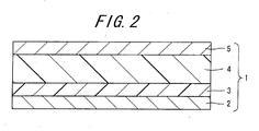
- Fig. 2 is a sectional view of an electromagnetic wave absorber 1 of an embodiment of the invention.
- an electromagnetic wave absorber 1 that improves an electromagnetic wave environment of a space such as an office, from an electromagnetic wave incident side that is an upper side in Fig. 2, a pattern layer 5, an electromagnetic wave absorbing layer 4, a dielectric layer 3 and a conductive reflective layer 2 are laminated in this order.
- the pattern layer 5 has a plurality of conductive patterns 12.
- the conductive pattern 12 depending on shapes of the respective patterns 30 and 31 contained in the conductive pattern 12, can control a matching frequency.
- the electromagnetic wave absorber 1 is used to absorb, for instance, an electromagnetic wave of 2.4 GHz or 5.2 GHz.
- Fig. 3 is a front view showing a pattern layer 5 that constitutes an electromagnetic wave absorber 1 of an embodiment of the invention shown in Fig. 2.
- Fig. 4 is a front view obtained by partially expanding a pattern layer 5 in an embodiment shown in Figs. 2 and 3.
- a conductive pattern 12 is formed on a surface on an electromagnetic wave incident side of a planar substrate 11.
- the planar substrate 11 is made of a dielectric that is for instance a synthetic resin and the planar substrate 11 as well is a dielectric loss material.
- the conductive pattern 12 has a radial pattern 30 and a substantially square pattern 31.
- the radial pattern 30 is formed in a radial shape and a plurality of radial patterns 30 are disposed separated from each other with separations (hereinafter, referred to as "radial pattern separation") c2x and c2y. More specifically stated, for instance, in the embodiment, the radial pattern 30 is formed in a cross shape that is radial along an x direction and a y direction that are perpendicular to each other and the radial patterns 30 may be regularly arranged in matrix with a radial pattern separation c2x disposed in an x direction and a radial pattern separation c2y disposed in a y direction.
- the radial pattern 30 has a shape where with a cross shape 20 shown with a virtual line in Fig. 4 as a basis, four corner portions 21 at an intersection 16 are formed in curve, specifically, in arc.
- the cross shape 20 that is a basis has a shape where a rectangular portion 14 slenderly extending in an x direction and a rectangular portion 15 slenderly extending in a y direction intersect at a right angle at the intersection 16 with gravity centers of the respective shape portions 14 and 15 superposed.
- the respective shape portions 14 and 15 are displaced by 90° from each other around a vertical axial line at the intersection 16 and have the same shape.
- four substantial triangles 22 each of which is a rectangular isosceles triangle and has a hypotenuse facing a right angle corner portion and concave toward the right angle corner portion are disposed so that the right angle corner portion may be accommodated in a corner portion 21 of the respective intersections 16 of the cross shape 20.
- widths a1x and a1y of the respective shape portions 14 and 15 are equal, for instance, 1.0 mm, and lengths a2x and a2y of the respective shape portions 14 and 15 are equal, for instance, 25.0 mm.
- a dimension to be an arc of a corner portion formed in arc accordingly, lengths of sides excluding a hypotenuse of a substantial triangle 22, specifically, a length a3x of a side in an x direction and a length a3y of a side in a y direction are same, for instance, 11.5 mm, and a curvature radius R1 of the hypotenuse is 11.5 mm.
- a separation c2x in an x direction and a separation c2y in a y direction are same, and, for instance, 4.0 mm.
- the substantially square pattern 31 is disposed in a region surrounded by radial patterns 30 with a separation (hereinafter, referred to as "radial-square separation" c1 distanced from the radial pattern 30 so as to fill in the region surrounded by the radial patterns 30.
- the substantially square pattern 31 is formed into a shape corresponding to the region surrounded by radial pattern portions. More specifically, in the embodiment for instance, the radial pattern portion 30 is formed in cross as mentioned above, the region surrounded by the radial patterns 30 is a substantial rectangle with a rectangle as a basis, and a shape corresponding thereto, that is, a radial-square separation c1 is formed in the same shape over an entire circumference.
- the region surrounded by the radial patterns 30 becomes a substantial square with a square as a basis
- the substantial square pattern 31 becomes a substantial square with a square 25 a basis.
- side portions of the square 25 that becomes a basis are disposed extended in either one of an x direction and a y direction.
- the substantial square pattern 31 has a shape where with a square 25 as a basis four corner portions 26 are formed in curve, specifically, in arc. Specifically, the substantial square pattern 31 has a shape where from the square 25 four substantial triangles 27 that are rectangular isosceles triangles and where a hypotenuse facing a right-angled corner portion is formed in arc concave toward the right-angled corner portion are removed with a positional relationship so that the right-angled corner portion may be housed in the respective corner portions 26 of the square.
- a dimension b1x in an x direction and a dimension b1y in a y direction of the square 25 are same and, for instance, 25.0 mm.
- a dimension to be an arc at a corner portion that is formed in arc accordingly, lengths of sides excluding a hypotenuse of the substantial triangle 27, specifically, a length b2x of a side in an x direction and a length b2y of a side in a y direction are same and, for instance, 10.0 mm, and a curvature radius R2 of the hypotenuse is 10.0 mm.
- a separation c1x in an x direction and a separation c1y in a y direction are same, and, for instance, 4.0 mm.
- Such radial pattern 30 and substantial square pattern 31 are conductive patterns having a substantial polygonal outline shape in which with a substantial polygon as a basis at least one corner portion is formed in curve. In such a pattern, a resonant current when an electromagnetic wave is received flows smoothly in a corner portion formed in curve.
- the radial pattern 30 and substantial square pattern 31 are not formed in line (in band) of a closed loop extending along an external peripheral border of the shape but are planar patterns of which internal peripheral portion is filled in. Accordingly, each of these can form a capacitor with the conductive reflective layer 2.
- the pattern layer 5 can efficiently receives electromagnetic waves having resonant frequencies of the respective conductive patterns 12.
- the final resonant frequency is determined influenced not only by the pattern dimension but also by the impedance that is determined from the coupling characteristics between the conductive patterns 12, the electromagnetic wave absorbing layer 4 and the dielectric layer 3.
- the electromagnetic wave absorbing layer 4 and the dielectric layer 3 are disposed; accordingly, energy of the electromagnetic wave received by the pattern layer 5 is lost.
- energy of the electromagnetic wave after converting into thermal energy, can be absorbed.
- the electromagnetic wave can be efficiently received and absorbed.
- the electromagnetic wave absorbing layer 4 is formed of a material that is at least one of a magnetic loss material having the complex specific permeability ( ⁇ ', ⁇ ") and a dielectric loss material having the complex specific permittivity ( ⁇ ', ⁇ ").
- the dielectric layer 3 is made of a dielectric loss material having the complex specific permittivity ( ⁇ ', ⁇ ").
- the conductive reflective layer 2 is formed on a surface on an incidence side of the electromagnetic wave of the planar substrate with a conductive film formed over an entire surface.
- the electromagnetic wave absorber 1 receives by the respective conductive patterns 12 of the pattern layer 5 electromagnetic waves of resonant frequencies determined by the shape and dimension thereof, and, allows losing the electromagnetic wave energy in the electromagnetic wave absorbing layer 4 and a loss layer including the dielectric layer 3, specifically, converts into thermal energy followed by absorbing.
- the electromagnetic wave absorber 1 can be formed as well without the dielectric layer 3.
- the electromagnetic wave absorber 1 When the electromagnetic wave absorber 1 is formed in a laminate configuration such as mentioned above, the absorption efficiency of the electromagnetic wave can be heightened and thereby the electromagnetic wave absorption characteristics large in the electromagnetic wave absorption amount can be obtained. Accordingly, the electromagnetic wave absorber 1 can achieve thinning and weight saving. In comparison with a configuration that absorbs an electromagnetic wave of, for instance, 2.45 GHz, the electromagnetic wave absorber 1 can realize the thinning where a thickness is suppressed to substantially 1/3 to substantially 1/4 that of a ⁇ /4 electromagnetic wave absorber, the thinning where a thickness is suppressed to substantially 1/2 that of a single layer electromagnetic wave absorber that uses rubber ferrite or the like, and the weight saving where a weight is suppressed to substantially 1/4. Furthermore, when the conductive pattern 12 is formed in planar pattern to form a capacitor with the conductive reflective layer 2 to make the capacitance larger, the receiving efficiency can be made higher and the electromagnetic wave absorption efficiency can be heightened.
- the electromagnetic wave absorber 1 is constituted disposed with a conductive reflective plate 2 as an electromagnetic wave shield plate.
- the electromagnetic wave absorber 1 is constituted so as to dispose on a surface of an object having the electromagnetic wave shielding properties. Thereby, determination of a shape and a dimension of the pattern shape 5, that is, designing becomes easy.
- resonant frequencies of the conductive patterns 12, 30 and 31 can be inhibited from varying under an influence of a disposition place of the electromagnetic wave absorber 1.
- the electromagnetic wave absorber 1 (of configuration in which a conductive reflective plate 2 is not laminated) is disposed on a building internal material that is not conductive, under influence of intrinsic complex specific permittivity of the internal material, a resonant frequency of the pattern (antenna) may be varied; however, this can be inhibited from occurring.
- the radial patterns 30 are disposed so as to confront radially extended portions each other as mentioned above, and the substantially square pattern 31 is formed in a shape corresponding to a region surrounded by the radial patterns 30.
- Such an arrangement is a combination where the radiant pattern 30 and the square pattern 31 that are different in the reception principle (a radial pattern is a dipole antenna and a square pattern is a patch antenna) are combined to optimize (become heighten) the reception efficiency. Accordingly, an electromagnetic wave absorber high in the absorption efficiency can be realized.
- the radial pattern 30 is disposed so as to radiate along an x direction and a y direction and side portions of a square that is a basis of the substantial square pattern 31 are disposed so as to extend in a x direction and a y direction; accordingly, electromagnetic waves polarized so that directions of electric fields may be present in a x direction and a y direction can be made higher in the receiving efficiency.
- the conductive pattern 12 that receives an electromagnetic wave has a substantial polygonal outline shape that is fundamentally a polygon and a peak value of an absorption amount of the electromagnetic wave can be made higher than that of a case where an outline shape of a conductive pattern is a circle.
- the conductive pattern 12 is formed fundamentally in a polygon with at least one corner portion thereof formed in curve. Thereby, a displacement of a frequency where an absorption amount becomes a peak depending on the polarization direction of an electromagnetic wave can be suppressed smaller.
- the conductive pattern 12 of the pattern layer 5 receives an electromagnetic wave having a particular frequency according to a resonation principle of antenna.
- the electromagnetic wave absorber of the invention in addition to absorbing the electromagnetic wave, has a function where the conductive pattern 12 effectively works, in a state where a metal (conductive reflective layer 2) is present in the vicinity thereof, as a receiving antenna as well.
- the particular frequency is a frequency determined by various elements such as a shape and a dimension of the conductive pattern 12 and a frequency to be absorbed by the electromagnetic wave absorber 1.
- a resonant current flows at an edge portion of the conductive pattern 12.
- the loss layer includes the electromagnetic wave absorbing layer 4 and the dielectric layer 3.
- a capacitor can be formed between the conductive pattern 12 of the pattern layer 5 and the conductive layer (a superficial layer or a conductive reflective layer of an object made of a conductive material).
- the capacitance of the capacitor can be made larger.
- a capacitor can be formed between patterns each other as well.
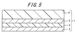
- Fig. 5 is a sectional view of an electromagnetic wave absorber 1 according to another embodiment of the invention.
- an electromagnetic wave absorbing layer 4 from an electromagnetic wave incidence side, an electromagnetic wave absorbing layer 4, a pattern layer 5, a dielectric layer 3 and a conductive reflective layer 2 are laminated in this order.
- Other configurations are same as that of the foregoing embodiment.
- an absorption amount of electromagnetic wave (amount of reflection loss) in the invention
- the computer simulation is carried out.
- the material constants and the thickness can select arbitrary combinations. For instance, in order to achieve more thinning, owing to a wavelength shortening effect by improving ⁇ ' or ⁇ ', one having a total thickness of 0.5 mm or 1.0 mm can as well be produced.
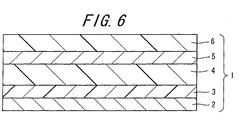
- Fig. 6 is a sectional view of an electromagnetic wave absorber 1 according to still another embodiment of the invention.
- portions similar and corresponding to embodiments of the Figs. 2 through 4 are shown with the same reference numerals.
- a superficial layer 6 may be further disposed on the electromagnetic wave incidence side of the pattern layer 5 (in the above of Fig. 6).
- the configuration is not restricted to ones shown in Figs. 5 and 6. For instance, one in which, from the electromagnetic wave incidence side, an electromagnetic wave absorbing layer 4, a pattern layer 5, an electromagnetic wave absorbing layer 4, a dielectric layer 3, and a conductive reflective layer 2 are formed in this order can be realized.
- Examples of the embodiments of the invention include a laminated body in which, from an incident direction of electromagnetic wave, a pattern layer 5, an electromagnetic wave absorbing layer 4, a dielectric layer 3 and a conductive reflective layer 2 are laminated in this order; a laminated body in which, from an incident direction of electromagnetic wave, an electromagnetic wave absorbing layer 4, a pattern layer 5, a dielectric layer 3 and a conductive reflective layer 2 are laminated in this order; a laminated body where an electromagnetic wave absorbing layer 4, a pattern layer 5, an electromagnetic wave absorbing layer 4, a dielectric layer 3 and a conductive reflective layer 2 are laminated in this order from an electromagnetic wave entrance direction; a laminated body in which a pattern layer 5, a dielectric layer 3 and a conductive reflective layer 2 are laminated in this order from an electromagnetic wave incidence direction; a laminated body where a pattern layer 5, a dielectric layer 3 and a conductive reflective layer 2 are laminated in this order from an electromagnetic wave incidence side; and the like.
- laminated bodies of various modes can be included. Furthermore, in the laminated bodies, only essential layers are extracted and the layers may not be necessarily arranged in the above orders. Even when, for instance, an adhesive layer, a support or a protective layer is inserted between the respective layers, an identical advantage can be obtained. Furthermore, when an adhesive is blended, an adhesive layer and a dielectric layer 3 or an electromagnetic wave absorbing layer 4 can be combined.
- an electromagnetic wave absorber may be configured, without containing the conductive reflective layer 2 in the respective embodiments of Figs. 2 through 6, so that such the electromagnetic wave absorber that does not contain the conductive reflective layer 2 may be disposed on a surface having the electromagnetic wave shielding properties on a side (downward in Figs. 5 and 6) opposite to the electromagnetic wave incidence side (upward in Figs. 5 and 6) of the dielectric layer3.
- the surface having the electromagnetic wave shielding properties may have a configuration similar to, for instance, the conductive reflective layer 2 and may be realized with for instance a metal plate or the like. Such a configuration can achieve the electromagnetic wave absorption characteristics similar to the electromagnetic wave absorber having the conductive reflective layer 2.
- Fig. 7 is a front view showing a pattern layer 5 that constitutes an electromagnetic wave absorber 1 of another embodiment of the invention.
- a pattern layer 5 shown in Fig. 7 is used in place of the pattern layer 5 shown in Figs. 3 and 4.
- Other configurations are same as the configurations of Figs. 2 through 6.
- the conductive pattern 12 of the pattern layer 5 shown in Figs. 3 and 4 has a radial pattern 30 and a substantially square pattern 31.
- a conductive pattern 12 of a pattern layer 5 of Fig. 7 has only a substantially square pattern 31. Even such a configuration can achieve a similar advantage.
- Fig. 8 is a front view showing a pattern layer 5 that constitutes an electromagnetic wave absorber 1 of still another embodiment of the invention.
- a pattern layer 5 shown in Fig. 8 is used in place of the pattern layer 5 shown in Figs. 3 and 4.
- Other configurations are same as the configurations of Figs. 2 through 6.
- the conductive pattern 12 of the pattern layer 5 shown in Figs. 3 and 4 has a radial pattern 30 and a substantially square pattern 31.
- a conductive pattern 12 of a pattern layer 5 of Fig. 8 has only a radial pattern 30. Even such a configuration can achieve a similar advantage.
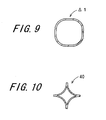
- Fig. 9 is a front view showing a substantially square pattern 41 of further still another embodiment of the invention.
- a substantially square pattern 41 shown in Fig. 9 is used in place of the substantially square patterns 31 in Figs. 3, 4 and 7, a substantially square pattern 41 shown in Fig. 9 is used.
- Other configurations are same as the configurations of Figs. 2 through 7.
- the substantially square patterns 31 shown in Figs. 3, 4 and 7 are planar patterns.
- the substantially square pattern 41 of Fig. 9 is a line-shaped (band-shaped) pattern of a closed loop extending along an external peripheral border. Even such a configuration, although a capacitance of a capacitor formed between with the conductive reflective layer 2 becomes smaller, can achieve a similar advantage.
- Fig. 10 is a front view showing a radial pattern 40 of another embodiment of the invention.
- a radial pattern 40 shown in Fig. 10 is used in place of the radial patterns 30 in Figs. 3, 4 and 8.
- Other configurations are same as the configurations of Figs. 2 through 6 and 8.
- the radial patterns 30 shown in Figs. 3, 4 and 8 are planar patterns.
- the substantially radial pattern 40 of Fig. 10 is a line-shaped (band-shaped) pattern of a closed loop extending along an external peripheral border. Even such a configuration, although a capacitance of a capacitor formed between with the conductive reflective layer 2 becomes smaller, can achieve a similar advantage.
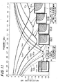
- Fig. 11 is a graph showing results of simulation of the absorption characteristics of electromagnetic waves.
- an electromagnetic wave absorber 1 a configuration of Fig. 2 is taken.
- a horizontal axis shows a frequency and a vertical axis shows the reflection loss.
- electromagnetic wave absorbers in which squares, substantial squares of which corner portions are formed in arc and circular patterns are arranged as shown in Fig. 7, the reflection characteristics are obtained. Except conditions of the curvature radii at corner portions, all conditions are same.
- lines 50a and 50b with a mark 50 show the electromagnetic wave absorption characteristics of a square pattern.
- lines 51a and 51b with a mark of 51 show the electromagnetic wave absorption characteristics of a circular pattern.
- lines 52a and 52b with a mark of 52 show the electromagnetic wave absorption characteristics of a pattern in which with a square as a basis corner portions are formed in arc with a small curvatureradius.
- lines 53a and 53b with a mark of 53 show the electromagnetic wave absorption characteristics of a pattern in which with a square as a basis corner portions are formed in arc with an intermediate curvatureradius.
- lines 54a and 54b with a mark of 54 show the electromagnetic wave absorption characteristics of a pattern in which with a square as a basis corner portions are formed in arc with a small curvature radius.
- the electromagnetic wave absorption characteristics to electromagnetic waves different by 45° in the polarization direction are shown differentiated with subscripts "a” and "b".
- the Q value is high and, although a peak value (peak absorption amount) of an absorption amount of electromagnetic wave is large, a frequency band where the absorption amount is large is narrow; accordingly, it is troublesome to match a frequency to an intended frequency to absorb. Furthermore, depending on the polarization direction of the electromagnetic wave, a frequency (peak frequency) where an absorption amount of electromagnetic wave becomes a peak is largely displaced; that is, the polarization characteristics are poor. In the circular pattern, the polarization characteristics are very excellent; however, since the Q value is small and a peak absorption amount is small. On the other hand, in the pattern (square with R) where with a square as a basis corner portions are formed in curve, a peak absorption amount is large and the polarization characteristics are excellent.
- a curve is formed with a curvature radius with a dimension as small as possible.
- a side length of a square 25 to which the substantially square patter 31 corresponds is 8 mm.
- the reflection loss is the loss when a viewpoint in that an electromagnetic wave entered in an electromagnetic wave absorber is reflected by the electromagnetic wave absorber is taken, expresses the loss when the electromagnetic wave is absorbed by the electromagnetic wave absorber and a value corresponding to an absorption amount of the electromagnetic wave in the electromagnetic wave absorber.
- the reflection loss is expressed with a minus value and an absolute value of the reflection loss becomes an absorption amount of the electromagnetic wave.
- Fig. 12 is a graph showing how the electromagnetic wave absorption characteristics vary with a dimension of a portion that is formed in curve at a corner portion in a conductive pattern in which with a square as a basis corner portions are formed in curve.
- Fig. 12 shows examples where when the corner portions of the conductive pattern are formed in curve, the Q values are increased, the reflection losses become larger, and the electromagnetic wave absorption characteristics are improved.
- a length of one side of the conductive pattern is set at 20 mm.
- the reflection loss of electromagnetic wave having 0° polarization is shown with a line 60, and a peak value is -23 dB (2.6 GHz).
- the reflection loss of electromagnetic wave having 0° polarization is shown with a line 61, and a peak value becomes -32 dB (2.65 GHz).
- the curvature radius R When the curvature radius R is further increased, this time, a value of the reflection loss becomes smaller and tendency of shifting toward a higher frequency is shown.
- the reflection loss of electromagnetic wave having 45° polarization is shown with a line 63
- the reflection loss of electromagnetic wave having 45° polarization is shown with a line 64
- the reflection loss of electromagnetic wave having 45° polarization is shown with a line 65
- the reflection loss of electromagnetic wave having 0° polarization is shown with a line 66
- the reflection loss of electromagnetic wave having 45° polarization is shown with a line 67.
- a dimension of a portion that is formed in curve at the corner portion is determined at a small dimension within the range of a dimension that can suppress the displacement of frequency of electromagnetic wave which can be absorbed due to the difference of the polarization direction.
- a portion that is formed in curve at the corner portion can be made as small as possible.
- a peak value of the absorption amount of the electromagnetic wave can be made as high as possible. That is, when the curvature radius R of a curve at the corner portion becomes larger, the pattern shape approaches a circle to be finally a circle.
- the Q value decreases and the electromagnetic wave absorption characteristics tend to deteriorate; however, the polarization characteristics are improved. Accordingly, when a dimension of a portion that is formed in curve at the corner portion is determined at a small dimension within the range of a dimension that can suppress displacement of frequency of electromagnetic wave which can be absorbed due to the difference of the polarization direction, a pattern shape where a magnitude of the curvature radius R is optimized so as to heighten the electromagnetic wave absorption characteristics but improve the polarization characteristics is formed. Accordingly, an electromagnetic wave absorber having very excellent electromagnetic wave absorption characteristics can be realized.
- Fig. 13 is a graph showing comparing calculated values and measurements of the electromagnetic wave absorption characteristics of an electromagnetic wave absorber 1 according to a pattern arrangement of Fig. 7 that uses a substantially square pattern 31 with R.
- a curve 70 shows calculated values of the electromagnetic wave absorption characteristics of an electromagnetic wave having 0° polarization and a curve 71 shows calculated values of the electromagnetic wave absorption characteristics of an electromagnetic wave having 45° polarization.
- a curve 72 shows measured values of the electromagnetic wave absorption characteristics of an electromagnetic wave of 0° polarized TE wave and a curve 73 shows measured values of the electromagnetic wave absorption characteristics of an electromagnetic wave of 0° polarized TM wave.
- a curve 74 shows measured values of the electromagnetic wave absorption characteristics of an electromagnetic wave of 45° polarization TE wave and a curve 75 shows measured values of the electromagnetic wave absorption characteristics of an electromagnetic wave of 45° polarization TM wave.
- the electromagnetic wave absorber 1 that uses the substantially square pattern 31 is designed so as to match an electromagnetic wave absorption peak to 2.45 GHz. According to calculation, the reflection loss of substantially -17 dB is obtained and the displacement of the absorption characteristics at 45° inclination is hardly found.
- the measured values are the electromagnetic wave absorption characteristics due to a free-space method in a state rotated by 0° and 45° to the TE wave and TM wave.
- the measured values of the reflection losses (corresponding to electromagnetic wave absorption amount) are in the range of -15 to -19 dB (including TE wave and TM wave and 0° and 45° polarizations) and small in the difference from the calculated values and measured values have a little larger bandwidth. Owing to impartation of R, the absorption characteristics excellent in the polarization characteristics are observed.
- Fig. 14 is a graph showing the electromagnetic wave absorption characteristics of an electromagnetic wave absorber 1 in which substantially square patterns 31 with R and different in size are arranged to intend to absorb the electromagnetic waves of two frequencies.
- Fig. 15 is a front view partially showing a conductive pattern showing the electromagnetic wave absorption characteristics of Fig. 14, specifically, an arrangement of substantially square pattern 31.
- conductive patterns different in outer peripheral length are combined to form.
- a first substantially square pattern 31a having a side length of a corresponding square 25 of 10 mm and a second substantially square pattern 31b having a side length of a corresponding square 25 of 24 mm are used, and a square pattern unit shown in Fig.
- the first substantially square patterns 31b are disposed in a checkered pattern, and, between the first substantially square patterns 31b, the second substantially square patterns 31a are disposed by four in matrix.
- a solid line 70 shows the electromagnetic wave absorption characteristics of 0° polarization and a broken line 71 shows the electromagnetic wave absorption characteristics of 45° polarization.
- the reflection loss (electromagnetic wave absorption characteristics) shows two absorption peaks of substantially -10 dB for both at 2.45 GHz and 5.2 GHz. Furthermore, when the absorption characteristics at 45° inclination are calculated, the displacement is hardly found. That is, an improvement effect of the R impartation can be assuredly confirmed.
- Table 1 shows comparing the electromagnetic wave absorption characteristics when substantially square patterns 31 having different curvature radii R are combined.
- Fig. 16 is a graph showing comparing the electromagnetic wave absorption characteristics when substantially square patterns 31 having different curvature radii R are combined.
- conductive patterns having different curvature radii at the corner portion are combined to form.
- the curvature radii R in a configuration where substantially square patterns 31 shown in Fig. 7 are arranged, between substantially square patterns 31 adjacent in an x direction and a y direction, the curvature radii R are different, and substantially square patterns 31 where the curvature radii R of the respective corner portions have a first value and substantially square patterns 31 where the curvature radii R of the respective corner portions have a second value are arranged in a checkered pattern. The first value and the second value are different.
- the curvature radius R though corresponding to the curvature radius R1 at the corner portion of the substantially square pattern 31 in Figs. 3 and 4 that are used in the explanation of Fig. 7, is expressed with "R" for the sake of convenience.
- Fig. 16 shows how the electromagnetic wave absorption characteristics become different when, in a configuration where substantially square patterns 31 are arranged as shown in Fig. 7, the curvature radii of the substantially square patterns 31 adjacent in an x direction and a y direction are varied.
- the respective lines 100 through 103 show the electromagnetic wave absorption characteristics of configurations where the respective corner portions of squares having a side length of 23 mm are formed in curve. A separation between squares is 6 mm.
- a broken line 100 shows the electromagnetic wave absorption characteristics when the curvature radii R of the substantially square patterns 31 adjacent in an x direction and a y direction are the same and 7 mm.
- a solid line 101 shows the electromagnetic wave absorption characteristics when among the substantially square patterns 31 adjacent in an x direction and a y direction, the curvature radii R of the respective corner portions of one substantially square patterns 31 are 6 mm and the curvature radii R of the respective corner portions of the other substantially square patterns 31 are 8 mm.
- a dotted line 102 shows the electromagnetic wave absorption characteristics when among the substantially square patterns 31 adjacent in an x direction and a y direction, the curvature radii R of the respective corner portions of one substantially square patterns 31 are 5 mm and the curvature radii R of the respective corner portions of the other substantially square patterns 31 are 9 mm.
- a chain line 103 shows the electromagnetic wave absorption characteristics when among the substantially square patterns 31 adjacent in an x direction and a y direction, the curvature radii R of the respective corner portions of one substantially square patterns 31 are 4 mm and the curvature radii R of the respective corner portions of the other substantially square patterns 31 are 10 mm.
- the broken line 100 shows the electromagnetic wave absorption characteristics of a configuration expressed by "one kind” in Table 1.
- the solid line 101 shows the electromagnetic wave absorption characteristics of a configuration expressed by "two kinds 1" in Table 1.
- the dotted line 102 shows the electromagnetic wave absorption characteristics of a configuration expressed by "two kinds 2" in Table 1 .
- the chain line 103 shows the electromagnetic wave absorption characteristics of a configuration expressed by "two kinds 3" in Table 1.
- widths of the absorption bands, respectively, show widths of frequency bands where the reflection loss is -20 dB, -15 dB, -10 dB and -6 dB.
- an absorption frequency of the electromagnetic wave shifts toward a lower frequency.
- the absorption frequency is a frequency where the absorption amount becomes a peak value.
- the peak value of the electromagnetic wave absorption amount is not so much lowered and the absorption frequency is shifted toward a lower frequency.
- the peak value of the electromagnetic wave absorption amount maintains the peak value of the absorption amount when the curvature radii R of two adjacent substantially square patterns 31 are same.
- the curvature radii R of two adjacent substantially square patterns 31 effectively contribute as a design parameter of an electromagnetic wave absorber. Owing to the interference and influence between adjacent conductive patterns, a peculiar phenomenon is caused. When a plurality of conductive patterns of which resonant frequencies caused by the difference of the curvature radii R at corner portions are near is combined, the absorption band and the resonant frequency can be varied. When the curvature radii R at corner portions of adjacent conductive patterns are differed, owing to an effect that the adjacent conductive patterns affect on each other, in comparison with a case where the curvature radii R at corner portions of the adjacent conductive patterns are made same, with the peak value of the absorption amount maintained, an absorption frequency can be altered.
- an absorption band can be varied. For instance, when a little difference is given to the curvature radii at corner portions of adjacent conductive patterns, without lowering the peak value of the absorption amount of the electromagnetic wave absorber, an absorption band can be expanded.
- absorption frequency a frequency of the electromagnetic wave to be absorbed
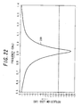
- Fig. 17 is a graph showing the electromagnetic wave absorption characteristics of an electromagnetic wave absorber 1 having a pattern layer 5 in which in a substantially square pattern 31 with R a void portion (slot antenna portion) 75 is disposed and in the void portion 75 a further smaller substantially square pattern 31 is disposed.
- Fig. 18 is a front view partially showing an arrangement of a conductive pattern showing the electromagnetic wave absorption characteristics of Fig. 17.
- a first substantially square pattern 31c wherein a substantially square (four corner portions are formed in curve) void portion 75 that has a side length of a corresponding square 25 of 24 mm and is in a direction tilted by 45° to an outline is formed and a second substantially square pattern 31d that is disposed in a direction same as the first substantially square pattern 31c and formed inside of the void portion 75 are disposed.
- a side length of the void portion 75 is 16 mm and a side length of the second substantially square pattern 31d is 10 mm.
- Fig. 17 calculation results of the reflection losses of an electromagnetic wave absorber 1 that uses a pattern layer 5 in which a plurality of pattern units shown in Fig. 18 is arranged repeating in an x direction and a y direction are shown.
- a solid line 80 shows the electromagnetic wave absorption characteristics of the 0° polarization
- a broken line 81 shows the electromagnetic wave absorption characteristics of the 45° polarization.
- the electromagnetic wave absorption is found at three bands corresponding to the respective antennas such as -3.5 dB at 1.8 GHz, -9 dB at 5.4 dB and -18 dB at 7.5 dB.
- the first substantially square pattern 31c that is a conductive pattern is provided with the void portion 75, and the void portion itself can be functioned as a receiving antenna. That is, in the substantially square pattern 31c resonant with a frequency corresponding to an external periphery length, a slot pattern (slot antenna portion) 75 resonant with a frequency corresponding to an internal periphery length can be disposed; accordingly, the substantially square pattern 31c that is one conductive pattern can resonate with a plurality (two or more) of different frequencies. Thereby, an electromagnetic wave absorber having bimodal characteristics that absorb electromagnetic waves of two frequencies respectively corresponding to an external periphery length of one conductive pattern and an internal periphery length of a slot pattern formed therein can be obtained.
- an electromagnetic wave absorber having the multi-modal characteristics in which, with one conductive pattern, electromagnetic waves of the number of the slot patterns + 1 of frequencies are absorbed can be obtained.
- another conductive pattern inside of the slot pattern, another conductive pattern can be disposed and this can be corresponded to another frequency of electromagnetic wave as a resonant antenna to further increase an absorption frequency. That is, by forming one slot pattern in one conductive pattern, an electromagnetic wave absorber having multi-modal characteristics that can theoretically absorb three or more frequencies of electromagnetic wave can be obtained. In this case as well, in addition to high absorption characteristics, when corner portions of the conductive pattern are formed in curve, the polarization characteristics can be improved. When the operation is repeated, further more (four or more) frequencies of electromagnetic wave can be absorbed.
- a producing method of an electromagnetic wave absorber 1 in the invention is for instance as follows.
- the electromagnetic wave absorbing layer 4 is formed by blending 100 parts of an SBS (styrene/butadiene/styrene copolymer) resin, 340 parts of ferrite and 50 parts of carbon black, followed by kneading together with other filler, further followed by sheeting in a thickness of 0.5 mm.
- SBS styrene/butadiene/styrene copolymer
- the dielectric layer 3 is formed by discharging inorganic and other fillers (magnetic loss material is not used) in an SBS (styrene/butadiene/styrene copolymer) resin, followed by kneading, further followed by sheeting in a thickness of 2.0 mm.
- SBS styrene/butadiene/styrene copolymer
- the material constants of the respective layers are, after forming into a ring of ⁇ 7 ⁇ ⁇ 3, measured by use of a network analyzer according to a coaxial tube method and the composition is controlled so as to obtain desired material constants.
- As other fillers a flame retardant, an antiaging agent, a working additive, inorganic filler and the like are appropriately used.
- the respective layers are laminated through an adhesive, followed by, after an adhering reaction comes to completion, cutting into a dimension of 50 cm x 50 cm.
- ferrites soft ferrites such as Mn-Zn ferrite, Ni-Zn ferrite, Mn-Mg ferrite and the like, or hard ferrite that is a permanent magnetic material
- iron alloys for instance, magnetic stainless (Fe-Cr-Al-Si alloy), sendust (Fe-Si-Al alloy), permalloy (Fe-Ni alloy), silicon copper (Fe-Cu-Si alloy), Fe-Si-B(-Cu-Nb) alloy, Fe-Si-Cr alloy, Fe-Ni-Cr-Si alloy and the like can be cited. These alloys can be used in flat shape.
- iron particles for instance, carbonyl iron powder can be cited.
- the carbonyl iron powder is preferred to be as spherical as possible.
- the shape without restricting to particular one, may be appropriately selected from any one shape of bulk shape, flat shape, fibrous shape or the like.
- soft ferrite powder cheap in the cost and high in the complex specific magnetic permeability can be used.
- the electromagnetic wave absorbing layer 4 may be formed of a magnetic body itself. In this case, a method where a layer of a soft magnetic sintered body such as ferrite, a plated matter thereof, a metal compound or a metal oxide is formed is adopted.
- a dielectric loss material contained in an electromagnetic wave absorbing layer 4 or, if necessary, in a dielectric layer 3 as well is an electromagnetic wave absorber that is a material selected from a group of graphite, carbon black, carbon fiber, graphite fiber, metal powder and metal fiber.
- the electromagnetic wave absorbing layer 4 necessarily contains a magnetic loss material.
- the electromagnetic wave absorbing layer 4 is preferably provided with appropriate complex specific permittivity.
- carbon black such as furnace black, channel black or the like, conductive particles or fibers of stainless steel, copper, aluminum and the like, graphite, carbon fiber, graphite fiber, titanium oxide and the like can be cited.
- the dielectric material preferably used in the invention is carbon black, in particular, carbon black that has the nitrogen absorption specific surface area (ASTM (American Society for Testing and Materials) D3037-93) in the range of 100 to 1000 m 2 /g and the DBP absorption (ASTM D2414-96) in the range of 100 to 400 ml/100g, for instance, IP1000 (trade name, produced by Showa Cabot Inc.) and Ketjen black EC (trade name, produced by Lion Aczo Co., Ltd.) can be preferably used.
- the DBP absorption means an absorption amount (unit: cm 3 /100g) of DBP (abbreviation of dibutyl phthalate) that is a kind of plasticizer.
- a synthetic resin, rubber and thermoplastic elastomer are used as a material (vehicle) of an organic polymer that is used in the electromagnetic wave absorbing layer 4 and the dielectric layer 3.
- a synthetic resin, rubber and thermoplastic elastomer are used as a material (vehicle) of an organic polymer that is used in the electromagnetic wave absorbing layer 4 and the dielectric layer 3.
- polyolefins such as polyethylene, polypropylene, copolymers thereof, polybutadiene, copolymers thereof and the like
- thermoplastic or thermosetting resins such as polyurethane, polyvinyl chloride, polyvinyl acetate, epoxy resin, phenol resin, melamine resin and the like and bitumen and the like can be cited.
- Resins having the viodegradability such as polyuric acid and the like can be used as well.
- the electromagnetic wave absorbing layer 4 and the dielectric layer 4 may be formed as a FRP in which glass fibers or the like are added.
- the electromagnetic wave absorbing layer 4 may be one obtained by impregnating a paint or the like having the magnetic property in, other than the organic polymers, plaster material, cement material, non-woven fabric, foamed body, paper, cardboard or the like.
- a material in which filler can be blended can be appropriately selected as well.
- the dielectric layer 3 is not restricted to one that uses an organic polymer, and, any materials, as far as these have the complex specific permittivity and do not show the electroconductivity,can be used. Forinstance, wood, plywood, paper, plaster, cement, clay, sand, soil, nonwoven fabric, recycle resin, nonflammable board, bitumen, asphalt, foamed body or the like can be used.
- the electromagnetic wave absorbing layer 4 may combine an adhesive layer. For instance, an epoxy resin and ferrite or a dielectric loss material are blended and can be placed in the respective interfaces of the pattern layer 5, dielectric layer 3 and conductive reflective layer 2 or between the respective layers when these are used in the lamination. In this case, as mentioned above, a configuration where the electromagnetic wave absorbing layer 4 and the dielectric layer 3 are alternately and repeatedly laminated can be taken.
- a nonflammable material and a flame resistant aide are added.
- the flame retardants without particularly restricting, phosphorus compounds, boron compounds, bromine based flame retardants, zinc based flame retardants, nitrogen based flame retardants, hydroxide based flame retardants and the like can be used in an appropriate amount.
- phosphorus compounds phosphoric acid esters, titanium phosphate and the like can be cited.
- boron compounds, zinc borate and the like can be cited.
- bromine based flame retardants hexabromobenzene, decabromobenzylphenyl ether, decabromobenzylphenyl oxide, tetrabromobisphenol, ammoniumbromide and the like can be cited.
- zinc based flame retardants zinc carbonate, zinc oxide, zinc borate and the like can be cited.
- nitrogen based flame retardants triazine compounds, hindered amine compounds, melamine compounds such as melamine cyanurate and melamine guanidine compounds and the like can be cited.
- hydroxide based flame retardants magnesium hydroxide, aluminum hydroxide and the like can be cited.
- a PET film that is used in the pattern layer 5 or the conductive reflective layer 2 isproblematic. Since,fundamentally,the PRTfilmisdifficult to render flame resistant, it is considered to cover with a nonflammable material such as char (carbonized layer).
- a flame resistant composition applied in the invention for the electromagnetic wave absorbing layer 4, to a base that contains 100 (phr) of PVC as a binder, 70 (phr) of calcium carbonate and 20 (phr) of a flame retardant (trade name: Nonesan SAN-l, produced by Maruzen Petrochemical Co., Ltd.), a dispersant, a plasticizer, ferrite, graphite and the like are blended. Furthermore, for the dielectric layer 3, 100 (phr) of recycled PVC as a binder, 140 (phr) of calcium carbonate, 10 (phr) of a flame retardant (trade name: Nonesan SAN-1, produced by Maruzen Petrochemical Co., Ltd.) and the like are blended. All layers show the flame resistance corresponding to V-0 of UL94.
- the pattern electromagnetic wave absorber prepared with the composition satisfies a fire prevention standard as a product.
- the pattern layer 5 and the conductive reflective layer 2 may be made of a metal such as gold, platinum, silver, nickel, chromium, aluminum, copper, zinc, lead, tungsten, iron and the like, a resin mixture in which in a resin, powder of the metal or conductive carbon black is mixed, a film of a conductive resin or the like.
- the foregoing metal or the like may be processed into a plate, sheet, film, nonwoven fabric or the like.
- a configuration where, on a synthetic resin film, a metal layer having a thickness of, for instance, 600 ⁇ is formed may be adopted.
- a metal foil may be transferred on a base such as a film, cloth or the like.
- conductive ink for instance, resistivity: 10 ⁇ /square or less and 0.5 ⁇ /square or more
- the electromagnetic wave absorption characteristics are measured by means of a free-space method.
- a plane wave is illuminated on an electromagnetic wave absorber 1 that is a sample to be measured placed in a free-space, the coefficient of reflection and coefficient of transmission at this time are measured by varying a frequency, an incident angle and the polarization to obtain the complex specific permittivity and the complex specific magnetic permeability ofamaterial. From thus obtained complexspecific permittivity and specific magnetic permeability, an electromagnetic wave absorption amount (reflection loss) of the electromagnetic wave absorber 1 is calculated to obtain. At this time, measurements are carried out of TE wave, TM wave and in a state where a sample is rotated by 45°.
- a used measurement instrument is a network analyzer (trade name: HP8720ES, produced by Agilent Technologies Inc.,) and an antenna is a double rigid antenna. Sizes of the respective sides of a rectangle of a measurement sample that is an electromagnetic wave absorber 1 are 500 ⁇ 500 (mm) and 1000 ⁇ 1000 (mm) .
- a surface layer 6 in Fig. 6 is may placed not only on one laminated in an order shown in Fig. 6 but also on an electromagnetic wave absorber 1 that is constituted in other order of lamination.
- Specific examples of the surface layer 6 include wallpaper, tile carpet, tile, flame resistant board, plywood, veneer, coated surface, resin plate, cloth, papers and the like.
- all materials other than conductive materials having the electromagnetic wave shielding property can be laminated thereon (outside of the pattern layer) . Even when these have a thickness such thin as 1 mm or less, the electromagnetic wave absorption characteristics are hardly affected. However, when these are thick or the complex specific permittivity thereof is high, redesigning is necessary to optimize the electromagnetic wave absorption characteristics. However, when these are redesigned and controlled, desired electromagnetic wave absorption characteristics can be exerted.
- An intended electromagnetic wave in the invention is an electromagnetic wave of at least part of frequency in for instance a 900-MHz band, more specifically, an electromagnetic wave of a frequency including a range of 950 MHz or more and 956 MHz or less.
- a frequency of an electromagnetic wave to be shielded is as exemplified and even a configuration that shields an electromagnetic wave of a frequency other than exemplified frequency is included in the invention.
- the 900-MHz band means a frequency range of 880 MHz or more and less than 1000 MHz.
- the material constants of the respective constituent layers vary without showing the difference in the frequency range and numerical values of the invention can be used as they are.
- the 2. 4-GHz band means an electromagnetic wave of 2400 MHz or more and less than 2500 MHz.
- the 2.4-GHz band is an electromagnetic wave of a frequency including a range of 2400 MHz or more and 2483.5 MHz or less for RFID.
- the electromagnetic wave to be absorbed includes an electromagnetic wave having a frequency of 300 MHz or more and 300 GHz or less.
- a pattern shape, a lamination structure and a composition of a pattern electromagnetic wave absorber having the absorption characteristics in a 950-MHz band are shown.
- a composition of the electromagnetic wave absorbing layer 4 with a basis of 100 (phr) of PVC (trade name: KS1700, produced by Kaneka Corp.), 430 (phr) of ferrite (trade name: LD-M, produced by JFE Ferrite Co., Ltd.) and 35 (phr) of graphite (trade name: Blue P, produced by Nihon Graphite Co., Ltd.), a plasticizer, a dispersant, calcium carbonate and the like are added.
- a pattern layer (aluminum-deposited PET film), an electromagnetic wave absorbing layer 4 (2.5 mm), plywood (6.5 mm) as a dielectric layer 3 and a conductive reflective layer (aluminum-deposited PET film) are laminated.
- Table 2 shows the electromagnetic wave absorption characteristics of TE wave and TM wave measured by use of a free-space method.
- TE Wave TM Wave Incident Angle 10° 30° 45° 10° 30° 45° Absorption Frequency (GHz) 0.95 0.95 1.00 0.95 1.05 1.05 Peak Value of Absorption Amount (dB) 20 20 16 25 30 22
- Fig. 19 is a graph showing the electromagnetic wave absorption characteristics of the TE wave measured by means of the free-space method.
- Fig. 20 is a graph showing the electromagnetic wave absorption characteristics of the TM wave measured by means of the free-space method.
- a solid line 110 shows the electromagnetic wave absorption characteristics when an incident angle is 10°
- a broken line 111 shows the electromagnetic wave absorption characteristics when an incident angle is 30°
- a chain line 112 shows the electromagnetic wave absorption characteristics when an incident angle is 45°.
- Fig. 19 is a graph showing the electromagnetic wave absorption characteristics of the TE wave measured by means of the free-space method.
- Fig. 20 is a graph showing the electromagnetic wave absorption characteristics of the TM wave measured by means of the free-space method.
- a solid line 110 shows the electromagnetic wave absorption characteristics when an incident angle is 10°
- a broken line 111 shows the electromagnetic wave absorption characteristics when an incident angle is 30°
- a chain line 112 shows the electromagnetic wave absorption characteristics when an incident angle
- a solid line 120 shows the electromagnetic wave absorption characteristics when an incident angle is 10°
- a broken line 121 shows the electromagnetic wave absorption characteristics when an incident angle is 30°
- a chain line 122 shows the electromagnetic wave absorption characteristics when an incident angle is 45°.
- the electromagnetic wave absorber having the abode-mentioned configuration shows the electromagnetic wave absorption amount of 20 dB to the TE wave incident at an incident angle of, for instance, 10° and the electromagnetic wave absorption of 25 dB to the TM wave incident at an incident angle of 10°. It is found that, while showing less anisotropicity, high absorption capacity is shown.
- an electromagnetic wave absorber 1 that absorbs an electromagnetic wave of 950 MHz can be obviously obtained.
- Fig. 21 is a front view showing a pattern layer 5 that constitutes an electromagnetic wave absorber 1 of still another embodiment of the invention.
- Fig. 22 is a graph showing the electromagnetic wave absorption characteristics of an electromagnetic wave absorber 1 provided with the pattern layer 5 shown in Fig. 21.
- a pattern shape, a lamination structure and a composition of a pattern electromagnetic wave absorber having the absorption characteristics in a 950-MHz band that shows further thinning will be shown.
- the pattern shape is, as shown in Fig. 21, substantially same as that shown in Fig. 3 except that only dimensions are different: Corresponding portions are shown with the same reference numerals.
- the respective curvature radii of the radial pattern 30 and substantially square pattern 31 are differentiated, and a separation c1 of two patterns 30 and 31 is continuously varied.
- c1 0.5 mm or more and 2.5 mm or less
- a separation c1 between the radial pattern 30 and the substantially square pattern 31 is continuously varied so that, in comparison with both end portions in a direction in which the separation between the patterns 30 and 31 extends, an intermediate portion may be larger.
- a composition of the electromagnetic wave absorbing layer 4 with a basis of 100 (phr) of chlorinated polyethylene (trade name: Elaslene 301NA, produced by Showa Denko K. K.) and 650 (phr) of carbonyl iron (trade name: EW-1, produced by BASF Co., Ltd.), aplasticizer, adispersant, calcium carbonate and the like are added.
- a pattern layer (aluminum-deposited PET film), an electromagnetic wave absorbing layer 4 (1.2 mm), a dielectric layer 3 (3.2 mm) and a conductive reflective layer (aluminum-deposited PET film) are laminated.
- the material constants of the electromagnetic wave absorber 4 and the dielectric layer 3 at 950 MHz are as shown in Table 3 below. That is, as an electromagnetic wave absorber of a 950-MHz band, a thin type having such a thickness as 4.4 mm (1.2 mm thick as a layer having the magnetic permeability) is realized.
- the electromagnetic wave absorption amount by simulation is as shown in Fig. 22. In Fig. 22, a line 200 shows the electromagnetic wave absorption amount. A result of the absorption of 19.5 dB in a 925-MHz band can be obtained.
- a configuration where a separation c1 between the radial pattern 30 and the substantially square pattern 31 that are adjacent two conductive patterns varies depending on a position can be formed.
- the electromagnetic wave absorption amount can be increased.
- the absorption frequency can be shifted toward a lower frequency and the absorption amount can be increased.
- Table 3 shows the material constants and thicknesses of the electromagnetic wave absorbing layers 4 and the dielectric layers 3 used in the embodiments.
- the electromagnetic wave absorbing layer 4 is simply expressed by "absorption layer”.
- the embodiments are only examples of the invention and the configuration can be varied within a range of the invention.
- the invention is characteristic in forming a corner portion of a conductive pattern in curve. However, there is no need of forming corner portions of all conductive patterns in curve but only corner portions of a part of the conductive patterns may be formed in curve. Furthermore, when an angle of the conductive pattern is formed in curve, all corner portions may be formed in curve or the corner portions may be partially formed in curve.
- the conductive pattern may be a substantially polygonal planar shape or a linear shape of a closed-loop extending along an external peripheral border of a substantially polygon.
- the electromagnetic wave absorbing layer can be configured containing at least one material selected from a group of ferrite, iron alloy and iron powder as a magnetic loss material at a blending amount of 1 parts by weight or more and 1500 parts by weight or less to 100 parts by weight of an organic polymer.
- the loss layer can be imparted with the complex specific magnetic permeability ( ⁇ ', ⁇ ") and thereby a magnetic field generated around the conductive pattern can be efficiently and energetically attenuated.
- a configuration where a real part ⁇ ' of the complex specific permittivity of the dielectric layer is in the range of 1 or more and 50 or less can be formed.
- the permittivities of the dielectric layer and the electromagnetic wave absorber can be arbitrarily controlled to contribute to the miniaturization of the conductive pattern and the thinning of the electromagnetic wave absorber.
- an electromagnetic wave absorber for absorbing an electromagnetic wave of a 2.4-GHz band a configuration having a total thickness of 4 mm or less can be formed.
- a conductive pattern can work as a resonant antenna to an electromagnetic wave of a 2.4-GHz band. Accordingly, the electromagnetic wave absorption efficiency in the electromagnetic wave absorber can be heightened and thereby the electromagnetic wave absorber can be thinned.
- an electromagnetic wave absorber for absorbing an electromagnetic wave of a 900-MHz band a configuration having a total thickness of 10 mm or less can be formed.
- a conductive pattern can work as a resonant antenna to an electromagnetic wave of a 900-MHz band. Accordingly, the electromagnetic wave absorption efficiency in the electromagnetic wave absorber can be heightened and thereby the electromagnetic wave absorber can be thinned.
- an electromagnetic wave absorber excellent as mentioned above an electromagnetic wave can be preferably absorbed.
- an electromagnetic wave environment can be improved.
- prevention of electronic machines (medical machines) frommalfunctioning due to the self-interference or the interference with other waves, protection of human bodies, countermeasures for transmission delay such as wireless LAN (2.4 GHz, 4.9 GHz, 5.2 GHz and the like), DSRC and ETC (5.8 GHz) and the like and countermeasures for preservation of electromagnetic wave transmission environments can be cited.
- an improvement in an electromagnetic wave transmission environment of wireless transmission between ITS-related mobile objects that uses an electromagnetic wave of a millimeter waveband can be cited as well.
- the electromagnetic wave environment without restricting to offices, general households, hospitals, concert halls, factories, research facilities, station houses, exhibition halls and outdoor facilities such as road sidewalls and the like can be cited.
- exhibition halls and outdoor facilities such as road sidewalls and the like.
- walls, floors, ceilings, pillars, panels, billboards, steel products and the like in the respective conceivable environments every necessary portions can be available.
- electromagnetic waves can be preferably absorbed.
- an electromagnetic wave absorber excellent in the electromagnetic wave absorption characteristics can be realized.
- a conductive pattern of a pattern layer receives an electromagnetic wave of a particular frequency according to a resonation principle of an antenna.
- the particular frequency is a frequency determined by various factors such as a shape and a dimension of the conductive pattern and the like and a frequency to be absorbed by an electromagnetic wave absorber. Since a loss layer is disposed laminated on the pattern layer having the conductive pattern that receives an electromagnetic wave,energy of the received electromagnetic wave can be lost with the loss layer. Thus, the electromagnetic wave can be absorbed.
- the conductive pattern that receives the electromagnetic wave is formed into an outline shape having a substantially polygonal shape that is fundamentally a polygon and has at least one corner portion thereof formed in curve.
- a displacement of a frequency where an electromagnetic wave absorption amount (hereinafter, in some cases, simply referred to as "absorption amount") becomes a peak value depending on the polarization direction of the electromagnetic wave can be suppressed small to improve the polarization characteristics.
- an electromagnetic wave absorber that is high in the peak value of the absorption amount of the electromagnetic wave and small in the displacement of the frequency where the absorption amount becomes a peak value depending on the polarization direction of the electromagnetic wave, that is, excellent in the electromagnetic wave absorption characteristics can be realized.
- the pattern layer may have a configuration where all conductive patterns have a curved corner portion or a configuration where all conductive patterns do not necessarily have a curved corner portion. That is, a configuration where a part of conductive patterns have a curved corner portion may be adopted. When a part of the conductive patterns have a curved corner portion, other conductive patterns are not restricted in whether these have a curved corner portion or not. Furthermore, in the conductive pattern having a curved corner portion, only a part of the corner portions may be formed in curve or all corner portions may be formed in curve. Still furthermore, the conductive pattern may be a substantially polygonal planar shape or a linear shape of a closed loop extending in a substantial polygon.
- a portion formed in curve at a corner portion can be formed as small as possible.
- a peak value of the absorption amount of the electromagnetic wave can be made as high as possible. That is, a pattern shape where a magnitude of the curvature radius R is optimized so that a peak value of absorption amount of electromagnetic wave may be high and the polarization characteristics may be improved is formed. Accordingly, an electromagnetic wave absorber very excellent in the electromagnetic wave absorption characteristics can be realized.
- an electromagnetic wave absorber when mounted on an object of which surface is made of a conductive material or a conductive reflective layer is further disposed to use in a state where the pattern layer is laminated on the conductive layer, a capacitor can be formed between the conductive pattern of the pattern layer and the conductive layer. Furthermore, since the pattern is formed in plane, a capacitance of a capacitor can be made larger. The planar conductive pattern tends to readily form a capacitor having a large capacitance. When the capacitor is formed, the reactance can be controlled, and thereby an electromagnetic wave absorber that uses the conductive pattern can be thinned.
- a conductive pattern works as a resonant antenna to an electromagnetic wave having a particular wavelength.
- a conductive pattern is designed so that an outer periphery length may correspond to a wavelength of a particular frequency. Accordingly, when conductive patterns different in outer periphery length are formed, the conductive patterns resonate with frequencies of two or more electromagnetic waves corresponding to the respective outer periphery lengths. Thereby, an electromagnetic wave absorber having the multi-modal characteristics that absorb electromagnetic wave having at least two frequencies of electromagnetic waves can be realized. In the case as well, not only the absorption characteristics can be heightened but also, when a corner portion of a pattern shape is formed in curve, the polarization characteristics can be improved.
- a frequency band of the electromagnetic wave to be absorbed (hereinafter, in some cases, referred to as "absorption band") can be altered.
- the alteration of the absorption band includes expanding the absorption band and alteration of the absorption frequency. For instance, when the curvature radii at corner portions of adjacent conductive patterns are a little differentiated, without lowering the peak value of the absorption amount of the electromagnetic wave absorber, the absorption band can be expanded.
- a frequency (hereinafter, in some cases, referred to as "absorption frequency”) of the electromagnetic wave to be absorbed can be lowered.
- an absorption amount of the electromagnetic wave in comparison with a case where a separation between two adjacent conductive patterns is formed with a definite value, an absorption amount of the electromagnetic wave can be made larger.
- a void portion is disposed in the conductive pattern and the void portion itself can be functioned as an antenna. That is, to the conductive pattern resonant with a frequency corresponding to an outer periphery length, a slot pattern (slot antenna) resonant with a frequency corresponding to an inner periphery length can be disposed to enable to resonate with a plurality (two or more) of different frequencies. Thereby, an electromagnetic wave absorber having the multi-modal characteristics that can absorb electromagnetic waves of at least two frequencies can be obtained.
- another conductive pattern can be disposed inside of the slot pattern and this can be corresponded as a resonant antenna to an electromagnetic wave having a separate frequency, and thereby an electromagnetic wave absorber having the multi-modal characteristics that can absorb theoretically electromagnetic waves having three or more frequencies can be obtained.
- an electromagnetic wave absorber having the multi-modal characteristics that can absorb theoretically electromagnetic waves having three or more frequencies can be obtained.
- the absorption characteristics can be heightened but also, when a corner portion of a pattern shape is formed in curve, the polarization characteristics can be improved.
- electromagnetic waves of further many frequencies (four or more) can be absorbed.
- the loss layer can be improved in the absorption of the electromagnetic wave. Accordingly, the electromagnetic wave absorption efficiency in the electromagnetic wave absorber can be improved and thereby the electromagnetic wave absorber can be thinned.
- the loss layer can be provided with the complex specific magnetic permeability ( ⁇ ', ⁇ "). Accordingly, a magnetic field generated around a conductive pattern can be efficiently energetically attenuated.
- the permittivities of the dielectric layer and the electromagnetic wave absorber can be arbitrarily controlled and thereby the miniaturization of the conductive pattern and the thinning of the electromagnetic wave absorber can be achieved.
- the surface resistivities (in accordance with JIS K6911) of the electromagnetic wave absorbing layer and the dielectric layer are sufficiently higher than a level that is called the electroconductivity (10 -4 to 10 1 ⁇ /square) and the layers do not have the electromagnetic wave shielding property.
- the electroconductivity (10 -4 to 10 1 ⁇ /square) a level that is called the electroconductivity (10 -4 to 10 1 ⁇ /square) and the layers do not have the electromagnetic wave shielding property.
- an electromagnetic wave of a particular frequency can be efficiently taken inside and can be converted to thermal energy.
- the electromagnetic wave, without being reflected can be preferably absorbed.
- an electromagnetic wave absorbing layer and a dielectric layer are constituted as a laminated body as well as a case where an electromagnetic wave absorbing layer and a dielectric layer are alternately laminated is supposed.
- the dielectric layer a thin plate of an nonflammable board, a thermosetting resin, flame resistant paper or a plywood is used, and, as an electromagnetic wave absorbing layer, an adhesive layer where a dielectric loss material is blended in an adhesive resin is used, in order to coat the adhesive layer thick to obtain a necessary thickness thereof, a dedicated unit becomes necessary to result in the cost increase.
- a conductive pattern can function as a resonant antenna with an electromagnetic wave of a 2.4-GHz band. Accordingly, the electromagnetic wave absorption efficiency in the electromagnetic wave absorber can be heightened and the electromagnetic wave absorber can be formed thinner.
- a conductive pattern can function as a resonant antenna with an electromagnetic wave of a 900-MHz band. Accordingly, the electromagnetic wave absorption efficiency in the electromagnetic wave absorber can be heightened and the electromagnetic wave absorber can be formed thinner.
- the electromagnetic wave absorber can be mounted on an obj ect a surface of which is made of a non-conductive material to absorb the electromagnetic wave. Accordingly, the convenience can be improved.
- the flame resistance or the nonflammability can be imparted to the electromagnetic wave absorber that is a laminated body.
- the flame resistance or the nonflammability may be imparted to, for instance, at least one layer of the electromagnetic wave absorbing layer and the absorbing layer to realize.
- the electromagnetic wave absorber can be preferably used as interior materials and materials that constitute the interior materials.
- an electromagnetic wave absorber excellent as mentioned above an electromagnetic wave can be preferably absorbed.
- the electromagnetic wave absorbers according to the respective inventions include, though only as an example, a floor material, a wall material and a ceiling material that form an electromagnetic wave environmental space such as offices, or a covering material of a metal surface of furniture and business machines, a partition or the like.
- electromagnetic wave absorbers according to the inventions are disposed to these applications, electromagnetic wave environments can be improved.
- the electromagnetic wave absorbers can be used to inhibit electronic machines (medical machines) from malfunctioning due to the self-interference or the interference with other waves and to protect human bodies from electromagnetic waves.
- the electromagnetic wave absorbers can be used as countermeasures for transmission delay, for preservation of electromagnetic wave transmission environments in wireless LAN (2.4 GHz, 4.9 GHz, 5.2 GHz and the like), IC tags (950-MHz band and 2.4-GHz band), DSRC and ETC (5.8 GHz) and marine lasers (9.4 GHz and 3 GHz) and the like and for inhibition of laser pseudo-image. Furthermore, an electromagnetic wave transmission environment of wireless transmission between ITS-related mobile objects that use an electromagnetic wave of a millimeter waveband can be improved as well.
- Examples of the electromagnetic wave environments include, without restricting to the offices, general households, hospitals, concert halls, factories, research facilities, station houses, exhibition halls, and outdoor facilities such as road sidewalls, ships, airplanes, containers, trucks, warehouses, distribution centers, department stores, parking lots, gasoline stands, convenience stores, stores and the like.
- the electromagnetic wave absorber can be used in every necessary portions such as walls, floors, ceilings, pillars, panels, billboards, steel products, desks, partitions, shelves, supports, instruments, metallic members and the like in the respective conceivable environment.
- the specific applications are only examples thereof and the invention, without restricting to the applications, can be widely used in all applications where the electromagnetic wave is intended to absorb.
Landscapes
- Physics & Mathematics (AREA)
- Electromagnetism (AREA)
- Engineering & Computer Science (AREA)
- Microelectronics & Electronic Packaging (AREA)
- Shielding Devices Or Components To Electric Or Magnetic Fields (AREA)
- Aerials With Secondary Devices (AREA)
Applications Claiming Priority (2)
| Application Number | Priority Date | Filing Date | Title |
|---|---|---|---|
| JP2004284968 | 2004-09-29 | ||
| PCT/JP2005/018036 WO2006035912A1 (fr) | 2004-09-29 | 2005-09-29 | Absorbeur d’ondes electromagnetiques |
Publications (2)
| Publication Number | Publication Date |
|---|---|
| EP1806961A1 true EP1806961A1 (fr) | 2007-07-11 |
| EP1806961A4 EP1806961A4 (fr) | 2009-06-24 |
Family
ID=36119059
Family Applications (1)
| Application Number | Title | Priority Date | Filing Date |
|---|---|---|---|
| EP05788222A Withdrawn EP1806961A4 (fr) | 2004-09-29 | 2005-09-29 | Absorbeur d'ondes electromagnetiques |
Country Status (5)
| Country | Link |
|---|---|
| US (1) | US7495181B2 (fr) |
| EP (1) | EP1806961A4 (fr) |
| KR (1) | KR20070085240A (fr) |
| CN (1) | CN101032198B (fr) |
| WO (1) | WO2006035912A1 (fr) |
Cited By (5)
| Publication number | Priority date | Publication date | Assignee | Title |
|---|---|---|---|---|
| DE102008051531A1 (de) * | 2008-10-14 | 2010-04-15 | Fraunhofer-Gesellschaft zur Förderung der angewandten Forschung e.V. | Vorrichtung zur Unterdrückung der Ausbreitung einer elektromagnetischen Störung in einem elektrischen System und ein elektrisches System mit derselben |
| EP2381756A3 (fr) * | 2010-04-26 | 2011-12-28 | Nitto Denko Corporation | Absorbeur d'ondes électromagnétiques |
| EP2118964A4 (fr) * | 2007-01-25 | 2013-06-05 | 3M Innovative Properties Co | Dispositif de protection électromagnétique |
| EP2898568B1 (fr) * | 2012-09-20 | 2018-11-14 | Universite Paris-Sud | Absorbant electromagnetique |
| CN112864633A (zh) * | 2021-01-08 | 2021-05-28 | 中南大学 | 一种基于超表面的宽带微波吸收体 |
Families Citing this family (54)
| Publication number | Priority date | Publication date | Assignee | Title |
|---|---|---|---|---|
| US7749024B2 (en) | 2004-09-28 | 2010-07-06 | Southwire Company | Method of manufacturing THHN electrical cable, and resulting product, with reduced required installation pulling force |
| US10763008B2 (en) | 2004-09-28 | 2020-09-01 | Southwire Company, Llc | Method of manufacturing electrical cable, and resulting product, with reduced required installation pulling force |
| WO2007046527A1 (fr) * | 2005-10-21 | 2007-04-26 | Nitta Corporation | Corps de tôle permettant d’améliorer la communication, dispositif d’antenne muni d’un tel corps de tôle et appareil de transmission d’informations électroniques |
| EP2144328B1 (fr) * | 2007-03-30 | 2017-11-01 | Nitta Corporation | Feuille améliorant des communications sans fil, étiquette à puce sans fil et système de communication sans fil utilisant la feuille améliorant des communications sans fil et l'étiquette à puce sans fil |
| DE102008002989A1 (de) * | 2007-08-16 | 2009-02-19 | Basf Se | Elektrisch leitfähiges, magnetisches Kompositmaterial, Verfahren zu seiner Herstellung und seine Verwendung |
| EP2221918A4 (fr) * | 2007-10-31 | 2012-07-11 | Nitta Corp | Matériau en feuille amélioré pour une communication sans fil, étiquette ci sans fil et système de communication sans fil utilisant le même matériau et la même étiquette |
| US9016002B2 (en) | 2008-03-06 | 2015-04-28 | Stuart Charles Segall | Relocatable habitat unit having interchangeable panels |
| US8677698B2 (en) | 2008-03-06 | 2014-03-25 | Stuart C. Segall | Relocatable habitat unit |
| US9157249B2 (en) | 2013-03-15 | 2015-10-13 | Stuart Charles Segall | Relocatable habitat unit |
| US20140109495A1 (en) * | 2008-03-06 | 2014-04-24 | Stuart Charles Segall | Relocatable habitat unit having radio frequency interactive walls |
| KR101042601B1 (ko) * | 2008-05-14 | 2011-06-20 | 한국전자통신연구원 | 저항성 재질을 이용한 공진형 전자파 흡수체 |
| KR100976857B1 (ko) * | 2008-06-04 | 2010-08-20 | 한국과학기술원 | 광대역 전자파 흡수체 및 그의 제조방법 |
| KR20100072383A (ko) * | 2008-12-22 | 2010-07-01 | 한국전자통신연구원 | 전자파 흡수체를 구비한 운송수단 용 자동 요금 징수 시스템, 운송용 장치, 건물형 구조물, 전자기기, 전자파 무반사실 |
| US8273997B2 (en) | 2009-01-16 | 2012-09-25 | The Boeing Company | Antireflective apparatus with anisotropic capacitive circuit analog sheets |
| US8986586B2 (en) | 2009-03-18 | 2015-03-24 | Southwire Company, Llc | Electrical cable having crosslinked insulation with internal pulling lubricant |
| EP2618339A3 (fr) * | 2010-03-12 | 2013-10-30 | General Cable Technologies Corporation | Câble doté d'une isolation avec des particules d'oxyde |
| CN102291967B (zh) * | 2010-06-15 | 2015-11-25 | 鸿富锦精密工业(深圳)有限公司 | 具有防电磁辐射功能开孔的壳体及具有该壳体的电子装置 |
| US9136043B2 (en) | 2010-10-05 | 2015-09-15 | General Cable Technologies Corporation | Cable with barrier layer |
| US9087630B2 (en) | 2010-10-05 | 2015-07-21 | General Cable Technologies Corporation | Cable barrier layer with shielding segments |
| FR2967306B1 (fr) * | 2010-11-05 | 2019-06-07 | Christian Lhomme | Tissu absorbant les ondes electromagnetiques |
| CN102211938B (zh) * | 2011-03-07 | 2013-03-20 | 中国人民解放军国防科学技术大学 | 一种碳化硅复合材料的吸波陶瓷及其制备方法 |
| US9307631B2 (en) * | 2013-01-25 | 2016-04-05 | Laird Technologies, Inc. | Cavity resonance reduction and/or shielding structures including frequency selective surfaces |
| US20140292460A1 (en) * | 2013-03-29 | 2014-10-02 | Samsung Electro-Mechanics Co., Ltd. | Inductor and method for manufacturing the same |
| WO2014198998A1 (fr) * | 2013-06-10 | 2014-12-18 | Nokia Corporation | Appareil de blindage et procédé de fabrication d'un appareil de blindage |
| WO2016010098A1 (fr) * | 2014-07-16 | 2016-01-21 | 日立金属株式会社 | Noyau magnétique, procédé de fabrication de noyau magnétique et composante de bobine |
| US10431350B1 (en) | 2015-02-12 | 2019-10-01 | Southwire Company, Llc | Non-circular electrical cable having a reduced pulling force |
| JP5996044B1 (ja) * | 2015-06-18 | 2016-09-21 | 日本特殊陶業株式会社 | スパークプラグ |
| CN106469857B (zh) * | 2015-08-20 | 2024-01-19 | 深圳光启尖端技术有限责任公司 | 吸波超材料 |
| CN105283058B (zh) * | 2015-11-24 | 2018-11-02 | 海南大学 | 一种电磁波吸收板及其制备方法 |
| KR102660419B1 (ko) * | 2016-04-19 | 2024-04-24 | 주식회사 에이치엘클레무브 | 레이더 장치 |
| CN106332536B (zh) * | 2016-08-26 | 2019-08-02 | 京东方科技集团股份有限公司 | 一种电磁干扰屏蔽结构 |
| CN106413367B (zh) * | 2016-09-05 | 2019-07-26 | 四川大学 | 一种多功能高分子基多层电磁屏蔽材料及其制备方法 |
| CN106572625A (zh) * | 2016-11-09 | 2017-04-19 | 上海无线电设备研究所 | 一种新型反射吸收一体化电磁屏蔽结构 |
| CN106714539A (zh) * | 2017-01-07 | 2017-05-24 | 深圳市景程信息科技有限公司 | 正四边形结构的电磁脉冲防护装置 |
| EP3606308B1 (fr) * | 2017-03-29 | 2023-11-15 | FUJIFILM Corporation | Absorbeur d'ondes électromagnétiques et procédé de production d'absorbeur d'ondes électromagnétiques |
| CN210610201U (zh) * | 2017-04-11 | 2020-05-22 | 株式会社村田制作所 | 电磁波屏蔽件、带电磁波屏蔽件的建材及带电磁波屏蔽件的物品 |
| CN109413971A (zh) * | 2017-08-15 | 2019-03-01 | 深圳富泰宏精密工业有限公司 | 屏蔽箱及射频衰减控制方法 |
| TWI783148B (zh) * | 2018-06-04 | 2022-11-11 | 日商麥克賽爾股份有限公司 | 電磁波吸收體 |
| US20200107479A1 (en) | 2018-09-27 | 2020-04-02 | Tdk Corporation | Metal magnetic film and magnetic sheet |
| RU189944U1 (ru) * | 2018-12-11 | 2019-06-11 | Государственное Унитарное Предприятие Республики Крым "Конструкторско-Технологическое Бюро "Судокомпозит" | Поглотитель электромагнитных волн |
| CN109802243B (zh) * | 2019-03-29 | 2021-08-24 | 北京环境特性研究所 | 一种基于afss的主被动兼容复合雷达吸收体 |
| CN112585009A (zh) * | 2019-06-07 | 2021-03-30 | 日东电工株式会社 | 电波吸收构件、电波吸收结构和检查装置 |
| CN110446412B (zh) * | 2019-08-09 | 2024-05-14 | 中国工程物理研究院流体物理研究所 | 一种用于探测器的丝阵式射频电磁屏蔽窗 |
| US11860394B1 (en) | 2019-09-25 | 2024-01-02 | Apple Inc. | Electronic devices with reduced stray light and ambient light reflections |
| CN110783712B (zh) * | 2019-10-27 | 2020-11-06 | 山西大学 | 一种超宽频带强电磁场防护装置 |
| CN111786128A (zh) * | 2020-06-03 | 2020-10-16 | 清华大学深圳国际研究生院 | 吸波结构、器件及其制备方法 |
| CN116457197A (zh) * | 2020-11-20 | 2023-07-18 | 凸版印刷株式会社 | 设计性电磁波抑制体、以及具备该设计性电磁波抑制体的建筑材料、电磁波抑制室及系统 |
| CN112582784B (zh) * | 2020-11-23 | 2022-03-15 | 华南理工大学 | 一种基于环加载和开槽的宽带基站天线及无线通信设备 |
| WO2022144638A1 (fr) * | 2020-12-29 | 2022-07-07 | 3M Innovative Properties Company | Composites absorbants électromagnétiques |
| CN113045263B (zh) * | 2021-03-18 | 2022-11-08 | 西南石油大学 | 一种混杂纤维水泥基泡沫复合吸波材料及其制备方法 |
| CN113067166B (zh) * | 2021-03-23 | 2024-04-12 | 广东顺德西安交通大学研究院 | 一种超薄耐高温宽频吸波体、吸波板及零件 |
| JP2023019268A (ja) * | 2021-07-29 | 2023-02-09 | Tdk株式会社 | ノイズ抑制シート |
| KR102626991B1 (ko) * | 2022-04-04 | 2024-01-23 | 한국항공우주산업 주식회사 | 표면 전류 제어용 시트 및 이의 제조 방법 |
| US20240251536A1 (en) * | 2022-12-23 | 2024-07-25 | Industrial Technology Research Institute | Electromagnetic wave absorber |
Family Cites Families (27)
| Publication number | Priority date | Publication date | Assignee | Title |
|---|---|---|---|---|
| US5223849A (en) * | 1986-11-25 | 1993-06-29 | Chomerics, Inc. | Broadband electromagnetic energy absorber |
| US5162809A (en) * | 1990-10-23 | 1992-11-10 | Hughes Aircraft Company | Polarization independent frequency selective surface for diplexing two closely spaced frequency bands |
| US5455116A (en) | 1992-10-27 | 1995-10-03 | Kansai Paint Co., Ltd. | Electromagnetic wave reflection-preventing material and electromagnetic wave reflection-preventing method |
| US5455117A (en) * | 1992-10-27 | 1995-10-03 | Kansai Paint Co., Ltd. | Electromagnetic wave reflection-preventing material and electromagnetic wave reflection-preventing method |
| JP3209456B2 (ja) | 1992-10-27 | 2001-09-17 | 関西ペイント株式会社 | 電波反射防止体および電波反射防止法 |
| US5453328A (en) | 1993-01-22 | 1995-09-26 | Kansai Paint Co., Ltd. | Electromagnetic wave reflection-preventing material and electromagnetic wave reflection-preventing method |
| JP3076473B2 (ja) | 1993-02-17 | 2000-08-14 | 関西ペイント株式会社 | 積層型電波反射防止体及び電波反射防止方法 |
| JP3417048B2 (ja) | 1994-04-08 | 2003-06-16 | ティーディーケイ株式会社 | 電波吸収体 |
| JP3776506B2 (ja) * | 1996-05-15 | 2006-05-17 | 株式会社竹中工務店 | 電磁波散乱吸収体及び電磁波散乱吸収方法 |
| JPH1154981A (ja) | 1997-08-01 | 1999-02-26 | Nippon Telegr & Teleph Corp <Ntt> | 電波吸収体 |
| JPH11204984A (ja) | 1998-01-14 | 1999-07-30 | Nippon Paint Co Ltd | 周波数選択性電磁波シールド材 |
| JP4474759B2 (ja) | 2000-09-05 | 2010-06-09 | 凸版印刷株式会社 | 複数の周波数選択性を有する電波遮蔽体 |
| JP4793521B2 (ja) | 2001-02-19 | 2011-10-12 | 大日本印刷株式会社 | 電波吸収体 |
| US6739028B2 (en) * | 2001-07-13 | 2004-05-25 | Hrl Laboratories, Llc | Molded high impedance surface and a method of making same |
| JP4857500B2 (ja) * | 2001-08-30 | 2012-01-18 | 凸版印刷株式会社 | 電波吸収体 |
| JP2003163487A (ja) * | 2001-09-17 | 2003-06-06 | Yoji Kozuka | 電磁波吸収減衰特性の改善方法 |
| JP4547849B2 (ja) * | 2001-12-10 | 2010-09-22 | 洋司 小塚 | 電波吸収体の特性変更方法 |
| JP4154942B2 (ja) | 2002-07-29 | 2008-09-24 | 凸版印刷株式会社 | フィルム型電磁波吸収体 |
| JP2004193531A (ja) * | 2002-12-09 | 2004-07-08 | Hiroki Kozuka | 電波反射抑制体およびその構成方法 |
| JP4235010B2 (ja) * | 2003-02-26 | 2009-03-04 | Tdk株式会社 | 不要電波抑制構造 |
| JP3647447B2 (ja) | 2003-05-28 | 2005-05-11 | ニッタ株式会社 | 電磁波吸収体 |
| TWM244562U (en) * | 2003-07-21 | 2004-09-21 | Via Tech Inc | Ground shield structure |
| JP4461974B2 (ja) * | 2004-02-27 | 2010-05-12 | 三菱瓦斯化学株式会社 | 電波吸収体 |
| JP2005244043A (ja) | 2004-02-27 | 2005-09-08 | Mitsubishi Gas Chem Co Inc | 電波吸収体 |
| EP1722618A4 (fr) * | 2004-03-01 | 2008-10-29 | Nitta Corp | Absorbeur d'ondes lectromagn tiques |
| US6967282B2 (en) * | 2004-03-05 | 2005-11-22 | Raytheon Company | Flip chip MMIC on board performance using periodic electromagnetic bandgap structures |
| JP2005288969A (ja) * | 2004-04-02 | 2005-10-20 | Nitsutakusu:Kk | 積層体および薄型建築材 |
-
2005
- 2005-09-29 CN CN2005800329573A patent/CN101032198B/zh not_active Expired - Fee Related
- 2005-09-29 US US11/664,101 patent/US7495181B2/en not_active Expired - Fee Related
- 2005-09-29 WO PCT/JP2005/018036 patent/WO2006035912A1/fr not_active Ceased
- 2005-09-29 EP EP05788222A patent/EP1806961A4/fr not_active Withdrawn
- 2005-09-29 KR KR1020077007262A patent/KR20070085240A/ko not_active Abandoned
Cited By (8)
| Publication number | Priority date | Publication date | Assignee | Title |
|---|---|---|---|---|
| EP2118964A4 (fr) * | 2007-01-25 | 2013-06-05 | 3M Innovative Properties Co | Dispositif de protection électromagnétique |
| DE102008051531A1 (de) * | 2008-10-14 | 2010-04-15 | Fraunhofer-Gesellschaft zur Förderung der angewandten Forschung e.V. | Vorrichtung zur Unterdrückung der Ausbreitung einer elektromagnetischen Störung in einem elektrischen System und ein elektrisches System mit derselben |
| DE102008051531B4 (de) * | 2008-10-14 | 2013-04-18 | Fraunhofer-Gesellschaft zur Förderung der angewandten Forschung e.V. | Elektrisches System mit einer Vorrichtung zur Unterdrückung der Ausbreitung einer elektromagnetischen Störung |
| EP2381756A3 (fr) * | 2010-04-26 | 2011-12-28 | Nitto Denko Corporation | Absorbeur d'ondes électromagnétiques |
| US8643531B2 (en) | 2010-04-26 | 2014-02-04 | Nitto Denko Corporation | Electromagnetic wave absorber |
| EP2898568B1 (fr) * | 2012-09-20 | 2018-11-14 | Universite Paris-Sud | Absorbant electromagnetique |
| CN112864633A (zh) * | 2021-01-08 | 2021-05-28 | 中南大学 | 一种基于超表面的宽带微波吸收体 |
| CN112864633B (zh) * | 2021-01-08 | 2022-03-04 | 中南大学 | 一种基于超表面的宽带微波吸收体 |
Also Published As
| Publication number | Publication date |
|---|---|
| EP1806961A4 (fr) | 2009-06-24 |
| US7495181B2 (en) | 2009-02-24 |
| US20080257599A1 (en) | 2008-10-23 |
| KR20070085240A (ko) | 2007-08-27 |
| CN101032198B (zh) | 2010-05-12 |
| CN101032198A (zh) | 2007-09-05 |
| WO2006035912A1 (fr) | 2006-04-06 |
Similar Documents
| Publication | Publication Date | Title |
|---|---|---|
| US7495181B2 (en) | Electromagnetic wave absorber | |
| JP3647447B2 (ja) | 電磁波吸収体 | |
| JP4108677B2 (ja) | 電磁波吸収体 | |
| KR101021188B1 (ko) | 전자파 흡수체 | |
| JP4073933B2 (ja) | 電磁波吸収体 | |
| JP4528334B2 (ja) | 電磁波吸収体 | |
| KR101166373B1 (ko) | 무선통신개선시트체, 무선통신 아이씨태그, 정보전달매체 및 무선통신시스템 | |
| EP2096711A1 (fr) | Corps de tôle permettant d améliorer la communication, dispositif d antenne muni d un tel corps de tôle et appareil de transmission d informations électroniques | |
| JP2009059972A (ja) | 電波吸収体、電波吸収パネル構造体、無線通信改善システム | |
| JP4181197B2 (ja) | シート体ならびにそれを備えるアンテナ装置および電子情報伝達装置 | |
| JP4833571B2 (ja) | 電磁波吸収体 | |
| JP5215579B2 (ja) | 電磁波吸収体、建材および電磁波暗室構造体ならびに送受信方向制御方法および電磁波吸収方法 | |
| JP2009043984A (ja) | 複合型電波吸収体 | |
| JP5085026B2 (ja) | 電磁波吸収体 | |
| JP4390058B2 (ja) | 携帯型無線通信装置用通信空間 | |
| JP4528318B2 (ja) | 電磁波吸収体および電磁波吸収方法 | |
| JP3141099B2 (ja) | 電磁シールド性能を備えたプラスチック系床材 | |
| JP2003174280A (ja) | 電磁波吸収体およびその製造方法ならびに電子機器 | |
| JPH06252583A (ja) | 電波遮蔽吸収パネル | |
| JP2005277373A (ja) | 電波吸収体 | |
| JP2006080609A (ja) | 平面アンテナ |
Legal Events
| Date | Code | Title | Description |
|---|---|---|---|
| PUAI | Public reference made under article 153(3) epc to a published international application that has entered the european phase |
Free format text: ORIGINAL CODE: 0009012 |
|
| 17P | Request for examination filed |
Effective date: 20070328 |
|
| AK | Designated contracting states |
Kind code of ref document: A1 Designated state(s): AT BE BG CH CY CZ DE DK EE ES FI FR GB GR HU IE IS IT LI LT LU LV MC NL PL PT RO SE SI SK TR |
|
| DAX | Request for extension of the european patent (deleted) | ||
| A4 | Supplementary search report drawn up and despatched |
Effective date: 20090527 |
|
| 17Q | First examination report despatched |
Effective date: 20090805 |
|
| GRAP | Despatch of communication of intention to grant a patent |
Free format text: ORIGINAL CODE: EPIDOSNIGR1 |
|
| RIC1 | Information provided on ipc code assigned before grant |
Ipc: H01Q 17/00 20060101ALI20120823BHEP Ipc: H01Q 15/00 20060101ALI20120823BHEP Ipc: H05K 9/00 20060101AFI20120823BHEP |
|
| RIN1 | Information on inventor provided before grant (corrected) |
Inventor name: KIYOHARA, YOSHIHARU, C/O NARA FACTORY OF NITTA COR Inventor name: SATO, SHINICHI, C/O NARA FACTORY OF NITTA CORPORAT Inventor name: MATSUSHITA, MASATO, C/O NARA FACTORY OF NITTA CORP Inventor name: YOSHIDA, TAKAHIKO, C/O NARA FACTORY OF NITTA CORPO Inventor name: GO, HARUHIDE, C/O NARA FACTORY OF NITTA CORPORATIO Inventor name: MAEZAWA, MAKOTO, C/O NARA FACTORY OF NITTA CORPORA |
|
| STAA | Information on the status of an ep patent application or granted ep patent |
Free format text: STATUS: THE APPLICATION IS DEEMED TO BE WITHDRAWN |
|
| 18D | Application deemed to be withdrawn |
Effective date: 20130208 |