EP1808825A2 - Bildlesevorrichtung - Google Patents
Bildlesevorrichtung Download PDFInfo
- Publication number
- EP1808825A2 EP1808825A2 EP06008212A EP06008212A EP1808825A2 EP 1808825 A2 EP1808825 A2 EP 1808825A2 EP 06008212 A EP06008212 A EP 06008212A EP 06008212 A EP06008212 A EP 06008212A EP 1808825 A2 EP1808825 A2 EP 1808825A2
- Authority
- EP
- European Patent Office
- Prior art keywords
- light
- irradiated
- irradiated object
- light source
- transmitting
- Prior art date
- Legal status (The legal status is an assumption and is not a legal conclusion. Google has not performed a legal analysis and makes no representation as to the accuracy of the status listed.)
- Withdrawn
Links
Images




Classifications
-
- G—PHYSICS
- G07—CHECKING-DEVICES
- G07D—HANDLING OF COINS OR VALUABLE PAPERS, e.g. TESTING, SORTING BY DENOMINATIONS, COUNTING, DISPENSING, CHANGING OR DEPOSITING
- G07D7/00—Testing specially adapted to determine the identity or genuineness of valuable papers or for segregating those which are unacceptable, e.g. banknotes that are alien to a currency
- G07D7/06—Testing specially adapted to determine the identity or genuineness of valuable papers or for segregating those which are unacceptable, e.g. banknotes that are alien to a currency using wave or particle radiation
- G07D7/12—Visible light, infrared or ultraviolet radiation
- G07D7/121—Apparatus characterised by sensor details
-
- G—PHYSICS
- G06—COMPUTING OR CALCULATING; COUNTING
- G06Q—INFORMATION AND COMMUNICATION TECHNOLOGY [ICT] SPECIALLY ADAPTED FOR ADMINISTRATIVE, COMMERCIAL, FINANCIAL, MANAGERIAL OR SUPERVISORY PURPOSES; SYSTEMS OR METHODS SPECIALLY ADAPTED FOR ADMINISTRATIVE, COMMERCIAL, FINANCIAL, MANAGERIAL OR SUPERVISORY PURPOSES, NOT OTHERWISE PROVIDED FOR
- G06Q20/00—Payment architectures, schemes or protocols
- G06Q20/04—Payment circuits
- G06Q20/042—Payment circuits characterized in that the payment protocol involves at least one cheque
Definitions
- the present invention relates to an image reading apparatus for reading an image of an irradiated object having a portion of reflecting and a portion of transmitting light as in a banknote or the like.
- JP-A-2000-113269 describes a banknote examining apparatus for examining a banknote or the like by irradiating light to a watermark pattern of a banknote or the like, detecting light transmitted therethrough by an artificial retina chip, and processing information of a shape or the like and presence or absence of an watermark image by a knowledge processing circuit.
- JP-A-2003-87564 describes an image reading apparatus using both of a so-to-speak transmitting type and reflecting type. Further, according to the image reading apparatus, there is described an image reading apparatus constituted such that a light source for a transmitting draft is contained in a draft cover, a draft mat is locked by the draft cover attachably thereto and detachably therefrom, whereas in reading a reflecting draft, the draft mat is mounted to the draft cover, in reading the transmitting draft, the draft mat is detached from the draft cover.
- the invention has been carried out in order to resolve the problem of the background art and it is an object thereof to provide a small-sized and efficient image reading apparatus constituted by combining a so-to-speak reflecting type and a transmitting type, capable of reading both of a reflecting portion and a transmitting portion of light of an irradiated object by carrying the irradiated object only once with regard to the irradiated object having the reflecting portion and the transmitting portion of light.
- an image reading apparatus includes a carrying unit that carries an irradiated object having a light reflecting portion and a light transmitting portion in a carrying direction, a first light source arranged on one face side of the irradiated object that irradiates light to a light irradiated portion in a path of carrying the irradiated object, a second light source arranged on other face side of the irradiated object that irradiates light to the irradiated portion, a detecting unit arranged to be spaced apart from the irradiated portion by a predetermined distance in a direction reverse to the carrying direction that detects the transmitting portion of the irradiated object, a lighting control unit that controls to put on the second light source during a time period of passing the transmitting portion through the irradiated portion by the detecting unit, a lens array arranged on the one face side of the irradiated object that converges reflecting light reflected by the reflecting portion
- an image reading apparatus includes a carrying unit that carries an irradiated object having a light reflecting portion and a light transmitting portion in a carrying direction, a first light source arranged on one face side of the irradiated object that irradiates light to a light irradiated portion in a path of carrying the irradiated object, a second light source arranged on other face side of the irradiated object that irradiates light to the irradiated portion, a detecting unit arranged to be spaced apart from the irradiated portion by a predetermined distance in a direction reverse to the carrying direction that detects the transmitting portion of the irradiated object, a lighting control unit that controls to put on the second light source during a time period of passing the transmitting portion through the irradiated portion by the detecting unit, a lens array arranged on the one face side of the irradiated object that converges reflecting light reflected by the reflecting portion
- the detecting unit is constituted by a light emitting element and a light receiving element and the irradiated object is carried between the light emitting element and the light receiving element.
- the carrying unit carries the irradiated object at a constant speed
- the lighting control unit puts on the second light source and puts off the first light source after an elapse of a constant time period from when the transmitting portion of the irradiated object is detected by the detecting unit.
- the plurality of detecting units are provided in a direction orthogonal to the direction of carrying the irradiated object, the second light source is divided in correspondence with respectives of the detecting unit and lighting is carried out by the lighting control unit for respective divided regions thereof.
- the second light source is an infrared ray light source.
- the checking unit compares a digital output signal constituted by converting the output signal of the sensor at the transmitting portion of the irradiated object by A/D conversion and an image signal of the transmitting portion of the irradiated object stored to a storing unit.
- the checking unit compares a digital output signal constituted by deleting a digital output signal at the transmitting portion of the irradiated object having a level equal to or smaller than a predetermined level and a digital image signal of the transmitting portion of the irradiated object stored to a storing unit.
- the checking unit includes an averaging unit that averages the output signal at the transmitting portion of the irradiated object.
- the checking unit includes a register that holds the digital output signals at respective scanning lines.
- the storing unit is stored with an image data of a black watermark portion or a white watermark portion, or an image data of a data of a region coated with a fluorescent ink.
- an image reading apparatus includes a carrying unit that carries an irradiated object having a light reflecting portion and a light transmitting portion and coated with a fluorescent ink at the transmitting portion in a carrying direction, a first light source arranged on one face side of the irradiated object that irradiates light to an irradiated portion of light in a path of carrying the irradiated object, a second light source arranged on other face side of the irradiated object that irradiates an ultraviolet ray to the irradiated portion, a detecting unit arranged to be spaced apart from the irradiated portion by a predetermined distance in a direction reverse to the carrying direction, a lighting control unit that controls to put on the second light source and put off the first light source during a time period of passing the transmitting portion through the irradiated portion by the detecting unit, a lens array that converges reflecting light reflected by the reflecting portion of the
- an image reading apparatus includes a carrying unit that carries an irradiated object having a light reflecting portion and a light transmitting portion and coated with a fluorescent ink at the transmitting portion in a carrying direction, a first light source arranged on one face side of the irradiated object that irradiates light to an irradiated portion of light in a path of carrying the irradiated object, an ultraviolet ray cut filter provided at the irradiated portion between the first light source and the irradiated object that removes an ultraviolet ray, a second light source arranged on other face side of the irradiated object that irradiates an ultraviolet ray to the irradiated portion, a detecting unit arranged to be spaced apart from the irradiated portion by a predetermined distance in a direction reverse to the carrying direction, a lighting control unit that controls to put on the second light source and put off the first light source during a time period of passing the transmitting portion
- Fig. 1 is a sectional constitution view of an image reading apparatus according to Embodiment 1 .
- Fig. 2 is a plane constitution view of the image reading apparatus.
- numeral 1 designates an irradiated object of, for example, a banknote, securities, a check or the like (hereinafter, simply referred to as "draft” or “banknote”) which includes a semitransparent or transparent watermark portion (hereinafter, also referred to as a transmitting portion) and a reflecting portion through which light is not transmitted.
- the transmitting portion is formed by a width which is constant in a direction of transmitting the draft 1 from one end over to other end in a direction orthogonal thereto.
- Numeral 2 designates a closely attached image sensor (hereinafter, simply referred to as "CIS") arranged on one face side (lower side of Fig. 1) of the draft 1.
- Numeral 3 designates a first light source (hereinafter, referred to as a reflecting type light source) arranged on both sides of CIS2, which is arranged on the one face side of the draft 1 and linearly aligned with LED chips in an array shape over a width direction (main scanning direction) of the draft 1.
- Numeral 4 designates a refractive type light guiding member for guiding light such that light emitted from each reflecting type light source 3 is irradiated to an irradiated portion 5 of the draft 1., which includes a light emitting section 4a.
- the irradiated portion 5 is a portion in a shape of a linear line in the main scanning direction at which light from the reflecting type light source 3 is irradiated to the draft 1 at a path of carrying the draft 1 and signifies a read portion of the carried draft 1.
- Numeral 6 designates a detecting unit (hereinafter, simply referred to as "photosensor") constituted by a separated type photosensor having a light emitting element 6a and a light receiving element 6b and is provided to extend from one to other end of the draft 1 in the main scanning direction of the draft 1.
- the photosensor 6 is provided with a connector 6c and is provided with a stay 7 for supporting the photosensor 6.
- the photosensor 6 although light emitted from the light emitting element 6a does not reach the light receiving element 6b by being reflected by a reflecting portion of the draft 1, with regard to the transmitting portion of the draft 1, the light reaches the light receiving element 6b by transmitting the transmitting portion. At this occasion, the photosensor 6 receives the light by the light receiving element 6b until the transmitting portion of the draft 1 finishes to pass.
- Numeral 8 designates a transmitting member having a function of preventing a foreign matter or the like from mixing into CIS2 and the draft 1 is carried by being guided by an outer side of the transmitting member 8.
- Numeral 9 designates a rod lens array by which after light emitted from the reflecting type light source 3 is reflected on the one face side of the draft 1, reflected light thereof is converged
- numeral 10 designates a light receiving section (sensor) that receives reflected light converged by the rod lens array 9 and is constituted by a sensor IC integrated with a plurality of photoelectric conversion sections, a drive circuit thereof and the like.
- Numeral 11 designates a sensor board mounted with a plurality of pieces of the light receiving sections (referred to also as sensor, sensor IC) 10
- numeral 12 designates a board constituted by a printed wiring board or the like mounted with the reflecting type light sources 3 on both sides thereof.
- Numeral 13 designates a signal processing IC (ASIC) integrated with a signal processing section including a correcting circuit for subjecting an analog signal photoelectrically converted by the light receiving section 10 to an A/D conversion and thereafter subjecting signal outputs of respective pixels (bits) to shading correction or all bits correction for outputting image information from the draft 1 as an image signal.
- Numeral 14 designates a connector supported by a back side of the board 12 for supplying power to a system signal (SCLK), a start signal (SI), a clock signal (CLK) and an input signal of a power source or the like and a light source or the like for driving CIS2, inputting and outputting a control signal and outputting an image signal (SIG) or the like to outside.
- SCLK system signal
- SI start signal
- CLK clock signal
- Numeral 15 designates an intermediate connector for delivering a signal between the sensor board 11 and the board 12
- numeral 16 designates an inner cabinet for containing and holding the rod lens array 9 and the sensor board 11
- numeral 17 designates an outer cabinet for containing and holding the refractive type light guiding member 4, the transmitting member 8 and the board 12. Further, the inner cabinet 16 is held by the intermediate connector 15.
- the reflecting type is constituted by the reflecting type light source 3, the rod lens array 9 and the light receiving section 10 and the like.
- numeral 20 designates a transmitting type light source member for emitting light in the main scanning direction of the draft 1.
- numeral 21 designates a second light source (hereinafter, referred to as transmitting type light source) linearly aligned with LED chips in an array shape in the main scanning direction
- numeral 22 designates a bugle type light guiding member for guiding light emitted from the transmitting type light source 21 to the draft 1, which includes a light emitting section 22a. Further, light emitted from the light emitting section 22a is constituted to be irradiated to the irradiated portion 5 in the path of carrying the draft 1.
- the irradiated portion 5 is made to coincide with the irradiated portion 5 irradiated by the reflecting type light source 3.
- Fig. 1 there is constructed a constitution of arranging the transmitting type light source 21, the rod lens array 9 and the light receiving section 10 on an optical axis of the transmitting type light source 21 such that light emitted from the transmitting type light source 21 is focused to the light receiving section 10 by way of the rod lens array 9.
- numeral 23 designates a transparent glass plate through which light transmits
- numeral 24 designates an LED board mounted with an LED chip of the transmitting type light source
- numeral 25 designates a connector supported by the LED board 24 for supplying power for driving the transmitting type light source
- numeral 26 designates a cabinet for containing and holding the bugle type light guiding member 22, the glass plate 23 and the LED board 24.
- the transmitting type is constituted by the transmitting type light source 21, the rod lens array 9 and the light receiving section 10 and the like.
- numeral 30 designates a carrying roller and is constituted by a sheet feeding side roller 30a, a sheet discharging side roller 30b, a take out roller 30c of the draft 1, a take in roller 30d of the draft 1.
- the carrying roller 30 carries the draft 1 by driving a motor (not illustrated) based on a predetermined carrying signal.
- Numeral 31 designates a cassette for containing the draft 1 and includes a sheet feeding side cassette 31a, a sheet discharging side cassette 31b.
- Numeral 32 designates a receiving base for fixing CIS2,
- numeral 33 designates a holder for fixing the detecting unit 6 including the photosensor and the second light source (transmitting type light source) 21.
- Numeral 34 designates a draft base for mounting the draft 1.
- the photosensor 6 is fixed to the stay 7.
- the draft 1 mounted on an upper section of the sheet feeding side cassette 31a is successively carried to the irradiated portion 5 of a reading region of CIS2 by the carrying rollers 30c, 30a.
- the photosensor 6 that detects the transmitting portion of the draft 1 provided with a black watermark, a white watermark or the like is installed to be spaced apart from the irradiated portion 5 by the predetermined distance L on the side reverse to the transmitting direction.
- the photosensor may be constituted by a single piece thereof.
- the banknote 1 passing the reading region is contained in the cassette 31b by the carrying rollers 30b, 30d.
- the carrying rollers 31a and 31b are driven in synchronism with each other such that the draft 1 is carried by a carrying speed of, for example, 250 mm/sec.
- notations the same as those of Fig. 1 designate the same or corresponding portions.
- the reflecting type light source 3 and the transmitting type light source 21, the photosensor 6 and the outer cabinet 17 and the like are fixed to a main body of an image reading apparatus (reading system) of, for example, a money terminal apparatus.
- the reflecting type light source 3 when the reflecting type light source 3 is put on during a time period of carrying the reflecting portion of the draft 1 through the irradiated portion 5, reflecting light reflected from the reflecting portion of the draft 1 at the irradiated portion 5 is focused to the light receiving section 10 by way of the rod lens array 9. At this occasion, the transmitting type light source 21 is put off.
- the transmitting type light source 21 is put on during a time period of carrying the transmitting portion of the draft 1 through the irradiated portion 5, transmitting light transmitted through a transmitting portion of the draft 1 is focused to the light receiving section 10 by way of the rod lens array 9. At this occasion, the reflecting type light source 21 is put off.
- the reflecting type light source 3 and the transmitting type light source 21 are put on and put off in this way, even when the transmitting type light source 21 is put on during a time period of putting the reflecting type light source on, light of the transmitting type light source 21 hardly effects an influence on reading the reflecting portion of the draft 1 even when the transmitting light source 21 is put on in a case in which the light is reflected by the reflecting portion of the draft 1 and is hardly received by the light receiving section 10 by way of the rod lens array 9.
- the reflecting type light source 3 when the reflecting type light source 3 is put on during the time period of putting the transmitting type light source 21 on, light of the reflecting type light source 3 transmits through the transmitting portion of the draft 1, however, there is a concern that a portion of the light is reflected by the transmitting portion of the draft 1 and is received by the light receiving section 10 and there is a possibility of effecting an influence on accurate reading at the transmitting portion of the draft 1. Therefore, in such a case, it is preferable to put the reflecting type light source 3 off during the time period of putting the transmitting type light source 21 on.
- Figs. 3A and 3B illustrate block constitution diagrams of the image reading apparatus according to Embodiment 1 .
- numeral 35 designates a light source driving circuit for putting on and putting off the reflecting type light source 3 and the transmitting type light source 21.
- Numeral 36 designates a control section (CPU) for controlling the light source driving circuit 35. That is, a timing signal of first detecting the transmitting portion of the draft 1 by the photosensor 6 is inputted to CPU 36.
- the light source driving circuit 35 is controlled to be driven by the timing to put on the transmitting type light source section 21, on the other hand, put off the reflecting type light source 3. Further, CPU 36 controls the light source driving circuit 35 to continue putting on the transmitting type light source 21 and putting off the reflecting type light source 3 by a time period of detecting the transmitting portion of the draft 1 by the photosensor 6.
- CPU 36 determines that the reflecting portion of the draft 1 passes and controls to drive the light source driving circuit 35 such that the reflecting type light source 3 is put on and the transmitting type light source 21 is put off. In this way, the reflecting type light source 3 and the transmitting type light source 21 are controlled to put on and put off by controlling to drive the light source driving circuit 35 by CPU 36.
- SCLK reading system signal
- numeral 37 designates a variable amplifier for amplifying an analog signal
- numeral 38 designates an A/D (analog to digital) converter for converting the analog signal into a digital signal
- numeral 39 designates a correcting circuit
- numeral 40 designates a checking circuit.
- notations the same as those of Fig. 1 and Fig. 2 designate the same or corresponding portions.
- Fig. 4 illustrates time chart diagrams showing a behavior of changing a relationship between an output signal (FO) of the photosensor 6 and lighting signals of the reflecting type light source 3 and the transmitting light source 21 with respect to a time axis.
- the draft 1 is assumed to be carried by, for example, 250 mm/sec.
- the output signal (FO) of the photosensor 6 is at a low level and therefore, the reflecting type light source 3 is put on (ON) and the transmitting type light source 21 is put off (OFF).
- the output signal (FO) of the photosensor 6 is at a high level.
- the reflecting type light source 3 is put off (OFF) and the transmitting type light source 21 is put on (ON) after, for example, 200 ms from a time point at which the output signal of the photosensor 6 rises in a predetermined level range of the output signal (FO) of the photosensor 6, that is, between Vth (L) and Vth (H) . Further, the output signal (FO) of the photosensor 6 continues only between Vth (L) and Vth (H).
- a total block constitution diagram shown in Fig. 3A will be explained.
- SI start signal
- CLK clock signal
- SO analog output
- the analog signal (SO) is amplified by the variable amplifier 37, thereafter, subjected to analog to digital (A/D) conversion by the A/D converter 38 and is inputted to the correcting circuit 39 and the checking circuit 40.
- A/D analog to digital
- digital data stored with previously set reference signal data is read from a region of RAM 1 and is subjected to an operation processing by image information sampled from the draft 1 and the correcting circuit 39.
- the operation is carried out for making the photoelectrically converted output by the light receiving section 10 uniform in consideration of dispersions in individual elements of the reflecting type light source 3 constituting the CIS 2, the rod lens array 9 and the light receiving section 10 or the like.
- the checking circuit 40 reads digital data in correspondence with a previously determined image pattern of the image signal at the transmitting portion of the draft 1 from RAM 2 and checks the digital data with image data at the transmitting portion which is actually read. That is, when the image at the transmitting portion of the draft 1 is read by putting on the transmitting type light source 21, as described above, the transmitting portion of the draft 1 is read by putting off the reflecting type light source 3 contained in CIS2, an illuminance provided in this way is photoelectircally converted by the light receiving section 10 to constitute an image output signal (SIG) . Further, the image output signal (SIG) is compared to check with the image data of the transmitting portion contained in RAM 2 and when the signal coincides with the image data, a coincidence signal (A) is outputted to outside.
- SIG image output signal
- transmitting light from the transmitting type light source 21 is direct light and therefore, an illuminance thereof is larger than an illuminance of light reflected by the reflecting type light source 3. Therefore, a lower limit of an output at the transmitting portion of the draft 1 is set, and an output larger than the set value output is taken out as line information of 1 line. This is illustrated as a waveform diagram extracted in Fig. 3A. The output larger than the set value output is checked for respective lines with regard to presence or absence of a portion similar to data contained in RAM 2 in this way.
- an average data of consecutive 4 bits is compared with data contained in RAM 2 and is determined with regard to a plurality of portions by a shape of an envelope of the digital data. Further, the operation is successively carried out for respective lines and when the coincidence signal (A) is generated over the plurality of lines, on the reading system side, true or false of the draft 11 is checked.
- Fig. 5 is an output waveform characteristic diagram with respect to a time axis showing the image output (SO) at a region of reading the draft 1 by the reflecting type light source 3 at each of 1 line of a reading period (0.5 ms) and the image output (SO) at a region of reading by the transmitting type light source 21.
- an output level of the image output (SO) of reading by the reflecting type light source 3 is low since scattered light from the draft 1 is received
- an output level of the image output (SO) of reading by the transmitting type light source 21 becomes high since direct light of the transmitting type light source 21 is received by transmitting the draft 1.
- change in the image data of the output superposed on direct light is compared with RAM 2 data with regard to similarity thereof by providing a constant threshold and therefore, detection of coincidence or incoincidence is facilitated by an image processing.
- a checking method will further be explained in reference to Figs. 3A and 3B.
- a size of the banknote 1 is normally equal to or smaller than 80 mm and therefore, in CIS having a specification of a resolution of 8 dots/mm, an effectively reading region of 640 bits is provided.
- the image output (SO) of the analog signal is converted into the digital output by the A/D conversion, subjected to the shading correction by the correcting circuit 39 and is transmitted to the reading system from SIG as the image output.
- the output of the correcting circuit 39 is commonly transmitted to the checking circuit 40 and the checking circuit 40 compares to check the watermark image arranged at the watermark region with the watermark image data previously contained in RAM 2.
- Fig. 6A is a digital output diagram expressing a digital output constituted by averaging the image data from the image output (SO) converted by the A/D conversion simply a unit of 4 bits.
- the A/D converter 38 having a resolution of 8 bits is used and therefore, the larger the numerical value, the larger the output by being expressed by 256 digits.
- Data for each line (1) inputted to the checking circuit 40 is first, operated to be processed to average and is contained in a register (shift register). According to Embodiment 1, bits of the register are 160 bits.
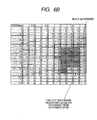
- a reference output is set to 180, a difference between the reference output and respective data is calculated and data equal to or smaller than 100 digits is deleted. (Fig. 6B).
- a minimum output of the watermark image is set (the reference output is -50 according to Embodiment 1), and an absolute value of the value is added to each output.
- RAM 2 is previously stored with image data of the black watermark portion shown in Fig. 7B to compare with the data of the watermark region transmitted for each line.
- image data contained in a bidirectional register is transmitted bidirectionally to compare with RAM 2 data (1) by utilizing a reading time period of a next line.
- a pixel position of CIS2 is specified and therefore, at the next line, data at the position of the specified pixel is transmitted to the shift register, latched, thereafter, compared with RAM 2 data (2) to check.
- the coincidence output (A) may be transmitted to the reading system at the time point, image data of next next line is similarly compared to check with RAM 2 data (3) to constitute a coincidence output.
- the image output from the image output (SO) is constituted by the output which is constituted by averaging 4 bits, this is because the watermark region image is regarded to be a comparatively coarse image. Further, because in irradiating from the transmitting type light source 21, the image is read by the direct light and therefore, the image output includes the output of the direct light. Further, the averaged output is constituted also in consideration of stain or the like of the watermark region. That is, the image of the watermark region is read to determine by a resolution of 2 bits/mm. Therefore, when the watermark image is determined by a higher density, an image with high accuracy can be read by adapting CIS having a resolution of 12 dots/mm.
- black watermark a portion having a thick thickness and dark watermark and white watermark (a portion having thin thickness) in the watermark region
- white watermark a portion having thin thickness
- the transmitting amount is high and therefore, by constituting check data of RAM 2 by data only of the white watermark region, even when the side of the reflecting type light source is brought into the lighted state, proper true or false determination can be carried out with regard to the watermark region.
- Figs. 8A to 8E illustrate explanatory views for explaining various watermark regions
- Fig. 8A shows a watermark region when a banknote having a rectangular watermark is carried in a longitudinal direction.
- Fig. 8B shows a watermark region when a banknote having a watermark in an elliptical shape is carried in a longitudinal direction.
- Fig. 8C shows a watermark region when a banknote having a rectangular watermark in a short side direction is carried. Therefore, according to a carrying method under a condition shown in Fig. 8C, substantially a total region of the banknote 1 becomes a watermark region, an image other than an inherent watermark region of the banknote 1 makes the reflecting type light source OFF and therefore, the watermark cannot be read.
- Embodiment 2 An explanation will be given thereof in Embodiment 2.
- FIG. 9 is a plane constitution view of an image reading apparatus according to Embodiment 2. According to Embodiment 2, an explanation will be given of a case of carrying the banknote 1 in a short side direction.
- 6 pieces of the photosensors 6 are installed to be spaced apart from each other by a predetermined interval, and the watermark region of the banknote 1 is specified by also dividing the inner circuit of the transmitting type light source 21 by 6. That is, as shown by Fig. 8D, the watermark region is divided into 6 portions with respect to the inherent watermark.
- the transmitting type light source 21 may be constituted to be divided by 6 respectively in correspondence with the photosensors 6 to be able to be put on individually.
- the reflecting type light source 3 is divided by, for example, 6 along the main scanning direction of the banknote 1 similar to the transmitting type light source 21, in the above-described case, by putting off the center portion of the reflecting type light source 3 and putting on the both end portions, also the reflecting portions of the both end portions of the transmitting portion of the banknote 1 are made to be able to be read.
- Embodiment 3 Although according to Embodiment 1 and Embodiment 2, the image is read and checked from a difference in the amount of transmitting light at the watermark portion of the banknote 1, an explanation in Embodiment 3 will be given of a case in which a fluorescent ink is provided to a watermark image or a case in which the watermark portion is printed with a pattern provided with the fluorescent ink.
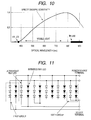
- Fig. 10 is a spectroscopic sensitivity diagram showing a spectroscopic sensitivity of the light receiving portion 10. According to a light receiving sensitivity of the light receiving section 10, the sensitivity is high on an infrared ray side and the sensitivity is low on an ultraviolet ray side. Further, Fig. 11 is a wiring diagram mounted with an infrared ray LED and an ultraviolet ray LED. According to Embodiment 3, an explanation will be given of a case of applying an ultraviolet ray LED (UV LED) having an optical wavelength ( ⁇ ) of 375 ⁇ 2 nm and being mounted with a transmitting member coated or printed with an ultraviolet ray cut filter on sale in place of the transmitting member 8 of Embodiments 1 and 2.
- UV LED ultraviolet ray LED
- Ultraviolet ray irradiated from the transmitting type light source 21 to a fluorescent ink coated on the watermark region of the banknote 1 is converted into visible light at a fluorescence region printed on the banknote 1 and is received by the light receiving section 10. Further, ultraviolet ray from the transmitting type light source 21 is blocked by the above-described transmitting member and therefore, the ultraviolet ray is not transmitted to the light receiving section 10. Further, as shown by Fig.
- fluorescent visible light shows the excellent light receiving sensitivity from purple to red color range and therefore, in driving the light source of Embodiment 3, by putting off visible light LED mounted to the reflecting type light source 3, not only presence or absence of the fluorescent ink or the like coated on the watermark region sufficiently but also true or false of an ink coating pattern can be detected by containing data of a region of coating the fluorescent ink in RAM 2 shown in Fig. 3A.
- the transmitting type light source 21 as shown by the wiring diagram of LED of Fig. 11, by constituting a group of 6 pieces mounted with infrared ray light sources (IR LED) and ultraviolet ray light sources, reading is carried out by dividing a reading region of the banknote 1 by 6.
- IR LED infrared ray light sources
- the transmitting type light source 21 by constituting a group of 6 pieces mounted with infrared ray light sources (IR LED) and ultraviolet ray light sources, reading is carried out by dividing a reading region of the banknote 1 by 6.
- IR LED infrared ray light sources
- ultraviolet ray light sources ultraviolet ray light sources
- ultraviolet ray of the transmitting type light source may include secondary visible light.
- the transmitting member coated with an ultraviolet ray cut filter is used, as shown by Fig. 10, the sensitivity of the light receiving section 10 with regard to ultraviolet ray is low and therefore, even when the ultraviolet ray cut filter is not used, true or false can be checked properly.
- Embodiments 1 and 2 by using the ultraviolet ray light source as the LED chip of the second light source 21, an output larger than other visible light LED of red, blue, green or the like can be provided, a photoelectrically converted output of the light receiving section 10 is increased and therefore, accuracy of reading the image and accuracy of determining true or false are promoted, a proper effect is achieved even when visible light LED is used for the transmitting type light source 21.
- LED of the reflecting type light source 3 the image can be read properly by using not only visible light but also infrared light by using a wavelength thereof pertinently at a plurality of wavelengths of 820 nm, 880 nm, 940 nm and the like.
Landscapes
- Health & Medical Sciences (AREA)
- General Health & Medical Sciences (AREA)
- Toxicology (AREA)
- Physics & Mathematics (AREA)
- General Physics & Mathematics (AREA)
- Business, Economics & Management (AREA)
- Accounting & Taxation (AREA)
- Strategic Management (AREA)
- General Business, Economics & Management (AREA)
- Engineering & Computer Science (AREA)
- Theoretical Computer Science (AREA)
- Image Input (AREA)
- Inspection Of Paper Currency And Valuable Securities (AREA)
- Facsimile Scanning Arrangements (AREA)
Applications Claiming Priority (1)
| Application Number | Priority Date | Filing Date | Title |
|---|---|---|---|
| JP2005358384A JP4320656B2 (ja) | 2005-12-13 | 2005-12-13 | 画像読取装置 |
Publications (2)
| Publication Number | Publication Date |
|---|---|
| EP1808825A2 true EP1808825A2 (de) | 2007-07-18 |
| EP1808825A3 EP1808825A3 (de) | 2008-05-07 |
Family
ID=37847038
Family Applications (1)
| Application Number | Title | Priority Date | Filing Date |
|---|---|---|---|
| EP06008212A Withdrawn EP1808825A3 (de) | 2005-12-13 | 2006-04-20 | Bildlesevorrichtung |
Country Status (4)
| Country | Link |
|---|---|
| US (1) | US7711175B2 (de) |
| EP (1) | EP1808825A3 (de) |
| JP (1) | JP4320656B2 (de) |
| CN (1) | CN1984221B (de) |
Families Citing this family (21)
| Publication number | Priority date | Publication date | Assignee | Title |
|---|---|---|---|---|
| JP4834968B2 (ja) * | 2004-08-11 | 2011-12-14 | 富士ゼロックス株式会社 | 真偽判定システム、真偽判定装置及びプログラム |
| JP2007003687A (ja) * | 2005-06-22 | 2007-01-11 | Canon Inc | 画像表示装置 |
| US7869799B2 (en) * | 2005-07-28 | 2011-01-11 | Research In Motion Limited | Method and system for forwarding calls placed to a telecommunications destination |
| JP4522952B2 (ja) * | 2006-01-18 | 2010-08-11 | 三菱電機株式会社 | 画像読取装置 |
| JP2007249475A (ja) | 2006-03-15 | 2007-09-27 | Mitsubishi Electric Corp | 画像読取装置及び紙幣読取方法 |
| JP2009284373A (ja) | 2008-05-26 | 2009-12-03 | Nippon Sheet Glass Co Ltd | 紫外線ライン照明装置、密着型イメージセンサ、画像読取装置および縮小光学系画像読取装置 |
| JP5227087B2 (ja) * | 2008-06-09 | 2013-07-03 | 日本金銭機械株式会社 | 紙葉類取扱装置 |
| JP4609531B2 (ja) * | 2008-06-11 | 2011-01-12 | 三菱電機株式会社 | 画像読取装置 |
| JP4609530B2 (ja) | 2008-06-11 | 2011-01-12 | 三菱電機株式会社 | 画像読取装置 |
| JP2010050689A (ja) * | 2008-08-21 | 2010-03-04 | Rohm Co Ltd | 画像読取装置 |
| JP5342197B2 (ja) * | 2008-08-26 | 2013-11-13 | ローム株式会社 | 画像読み取り装置 |
| JP5396660B2 (ja) * | 2009-01-08 | 2014-01-22 | 独立行政法人 国立印刷局 | 印刷物の品質検査装置 |
| JP5067638B2 (ja) * | 2009-04-13 | 2012-11-07 | Necエンジニアリング株式会社 | 画像読取装置 |
| CN102024286A (zh) * | 2011-01-12 | 2011-04-20 | 北京新岸线软件科技有限公司 | 一种纸币、票券的鉴别方法及装置 |
| WO2013022060A1 (ja) * | 2011-08-09 | 2013-02-14 | キヤノン・コンポーネンツ株式会社 | イメージセンサユニット及びこれを用いた画像読取装置 |
| JP5536150B2 (ja) | 2011-08-09 | 2014-07-02 | キヤノン・コンポーネンツ株式会社 | イメージセンサユニット及び画像読取装置 |
| JP2013083528A (ja) * | 2011-10-07 | 2013-05-09 | Vienex Corp | 密着型光学ラインセンサ装置及び有価紙面の鑑別方法 |
| JP5518820B2 (ja) * | 2011-10-21 | 2014-06-11 | キヤノン・コンポーネンツ株式会社 | イメージセンサユニットおよび画像読取装置 |
| CN103414838B (zh) * | 2013-06-20 | 2015-12-23 | 威海华菱光电股份有限公司 | 图像扫描装置及其控制方法 |
| WO2015186566A1 (ja) * | 2014-06-02 | 2015-12-10 | 株式会社ヴィーネックス | ライン光源及び光ラインセンサユニット |
| JP6395988B1 (ja) * | 2017-06-28 | 2018-09-26 | 三菱電機株式会社 | 導光体及び画像読取装置 |
Family Cites Families (22)
| Publication number | Priority date | Publication date | Assignee | Title |
|---|---|---|---|---|
| CH440786A (fr) * | 1965-06-02 | 1967-07-31 | Giori Gualtiero | Installation de contrôle et d'emballage des billets de banque |
| JPS5957107A (ja) * | 1982-09-27 | 1984-04-02 | Toshiba Corp | 紙葉類の損傷判定方式 |
| KR890002004B1 (ko) * | 1984-01-11 | 1989-06-07 | 가부시끼 가이샤 도오시바 | 지폐류 판별장치 |
| JPS6320576A (ja) | 1986-07-15 | 1988-01-28 | Omron Tateisi Electronics Co | 媒体認識装置 |
| JP2784138B2 (ja) * | 1993-12-09 | 1998-08-06 | 三菱電機株式会社 | イメージセンサ |
| IT1269506B (it) | 1994-02-04 | 1997-04-01 | De La Rue Giori Sa | Impianto di controllo di qualita' di fogli stampati in particolare di carte-valore |
| GB2309299B (en) * | 1996-01-16 | 2000-06-07 | Mars Inc | Sensing device |
| JP2000113269A (ja) | 1998-10-02 | 2000-04-21 | Mitsubishi Electric Corp | 紙幣鑑別装置 |
| JP3535040B2 (ja) | 1999-05-19 | 2004-06-07 | ローレルバンクマシン株式会社 | 紙幣判別装置 |
| JP3897939B2 (ja) * | 1999-09-28 | 2007-03-28 | 株式会社日本コンラックス | 紙葉類の識別方法および装置 |
| EP1316073B1 (de) * | 2000-08-31 | 2022-12-14 | Bundesdruckerei GmbH | Vorrichtung zur prüfung von beglaubigten dokumenten |
| CN1397910A (zh) * | 2001-07-17 | 2003-02-19 | 力捷电脑股份有限公司 | 可检测文件稿的扫描方法 |
| JP3918479B2 (ja) | 2001-09-11 | 2007-05-23 | セイコーエプソン株式会社 | シェーディング補正の基準データ設定方法及び画像読み取り装置 |
| DE10243051A1 (de) | 2002-09-17 | 2004-03-25 | Giesecke & Devrient Gmbh | Verfahren und Pfüfeinrichtung zur Prüfung von Wertdokumenten |
| JP2004227093A (ja) | 2003-01-20 | 2004-08-12 | Asahi Seiko Kk | 紙幣識別装置における紙幣検出装置 |
| JP4012853B2 (ja) * | 2003-04-23 | 2007-11-21 | アルゼ株式会社 | 貨幣取扱装置 |
| JP2004326624A (ja) | 2003-04-25 | 2004-11-18 | Aruze Corp | 識別センサ |
| JP4334911B2 (ja) | 2003-05-28 | 2009-09-30 | ローレル精機株式会社 | 紙幣画像検出装置 |
| JP3983206B2 (ja) * | 2003-08-21 | 2007-09-26 | 日本板硝子株式会社 | 画像読取装置 |
| JP3829853B2 (ja) * | 2004-03-31 | 2006-10-04 | 三菱電機株式会社 | イメージセンサ |
| US20060057467A1 (en) * | 2004-09-16 | 2006-03-16 | Fuji Photo Film Co., Ltd. | Hologram recording material and hologram recording method |
| GB0501568D0 (en) * | 2005-01-25 | 2005-03-02 | Innovative Technology Ltd | Improvements relating to banknote validation |
-
2005
- 2005-12-13 JP JP2005358384A patent/JP4320656B2/ja not_active Expired - Fee Related
-
2006
- 2006-04-10 US US11/400,201 patent/US7711175B2/en not_active Expired - Fee Related
- 2006-04-20 EP EP06008212A patent/EP1808825A3/de not_active Withdrawn
- 2006-06-01 CN CN2006100923515A patent/CN1984221B/zh not_active Expired - Fee Related
Also Published As
| Publication number | Publication date |
|---|---|
| CN1984221B (zh) | 2011-06-15 |
| JP2007164385A (ja) | 2007-06-28 |
| JP4320656B2 (ja) | 2009-08-26 |
| CN1984221A (zh) | 2007-06-20 |
| EP1808825A3 (de) | 2008-05-07 |
| US7711175B2 (en) | 2010-05-04 |
| US20070133858A1 (en) | 2007-06-14 |
Similar Documents
| Publication | Publication Date | Title |
|---|---|---|
| US7711175B2 (en) | Image reading apparatus | |
| US8837025B2 (en) | Image reading device | |
| EP2290622B1 (de) | Lichterkennungsvorrichtung und Blattverarbeitungsvorrichtung damit | |
| US6603126B2 (en) | UV/fluorescence detecting apparatus and sensing method thereof | |
| EP1049055B1 (de) | Bilderfassungsgerät mit Mehrwellenlängen-Lichtquellen und Verfahren zur Kontrolle desselben | |
| EP1818876A1 (de) | Bildlesevorrichtung | |
| US8264746B2 (en) | Image sensor | |
| US6881962B2 (en) | Paper fluorescence detection sensor | |
| US6359287B1 (en) | Apparatus for detecting an edge of a document | |
| US20020002410A1 (en) | Information acquisition method and apparatus | |
| JP2011118457A (ja) | 光検出装置、及びこの光検出装置を備える紙葉類処理装置 | |
| JP5093200B2 (ja) | 画像読取装置 | |
| EP4109384A1 (de) | Optischer sensor, papierbogenidentifizierungsvorrichtung und papierbogenverarbeitungsvorrichtung | |
| JP5056892B2 (ja) | 画像読取装置 |
Legal Events
| Date | Code | Title | Description |
|---|---|---|---|
| PUAI | Public reference made under article 153(3) epc to a published international application that has entered the european phase |
Free format text: ORIGINAL CODE: 0009012 |
|
| AK | Designated contracting states |
Kind code of ref document: A2 Designated state(s): AT BE BG CH CY CZ DE DK EE ES FI FR GB GR HU IE IS IT LI LT LU LV MC NL PL PT RO SE SI SK TR |
|
| AX | Request for extension of the european patent |
Extension state: AL BA HR MK YU |
|
| PUAL | Search report despatched |
Free format text: ORIGINAL CODE: 0009013 |
|
| AK | Designated contracting states |
Kind code of ref document: A3 Designated state(s): AT BE BG CH CY CZ DE DK EE ES FI FR GB GR HU IE IS IT LI LT LU LV MC NL PL PT RO SE SI SK TR |
|
| AX | Request for extension of the european patent |
Extension state: AL BA HR MK YU |
|
| 17P | Request for examination filed |
Effective date: 20081105 |
|
| AKX | Designation fees paid |
Designated state(s): DE GB IT |
|
| 17Q | First examination report despatched |
Effective date: 20110527 |
|
| STAA | Information on the status of an ep patent application or granted ep patent |
Free format text: STATUS: THE APPLICATION IS DEEMED TO BE WITHDRAWN |
|
| 18D | Application deemed to be withdrawn |
Effective date: 20151103 |