EP1808910A2 - Composant électronique doté dýau moins un dispositif de couche organique - Google Patents
Composant électronique doté dýau moins un dispositif de couche organique Download PDFInfo
- Publication number
- EP1808910A2 EP1808910A2 EP06026743A EP06026743A EP1808910A2 EP 1808910 A2 EP1808910 A2 EP 1808910A2 EP 06026743 A EP06026743 A EP 06026743A EP 06026743 A EP06026743 A EP 06026743A EP 1808910 A2 EP1808910 A2 EP 1808910A2
- Authority
- EP
- European Patent Office
- Prior art keywords
- layer
- anode
- cathode
- semiconductor material
- organic
- Prior art date
- Legal status (The legal status is an assumption and is not a legal conclusion. Google has not performed a legal analysis and makes no representation as to the accuracy of the status listed.)
- Granted
Links
Images
Classifications
-
- H—ELECTRICITY
- H10—SEMICONDUCTOR DEVICES; ELECTRIC SOLID-STATE DEVICES NOT OTHERWISE PROVIDED FOR
- H10K—ORGANIC ELECTRIC SOLID-STATE DEVICES
- H10K50/00—Organic light-emitting devices
- H10K50/10—OLEDs or polymer light-emitting diodes [PLED]
- H10K50/14—Carrier transporting layers
- H10K50/15—Hole transporting layers
- H10K50/155—Hole transporting layers comprising dopants
-
- B—PERFORMING OPERATIONS; TRANSPORTING
- B82—NANOTECHNOLOGY
- B82Y—SPECIFIC USES OR APPLICATIONS OF NANOSTRUCTURES; MEASUREMENT OR ANALYSIS OF NANOSTRUCTURES; MANUFACTURE OR TREATMENT OF NANOSTRUCTURES
- B82Y10/00—Nanotechnology for information processing, storage or transmission, e.g. quantum computing or single electron logic
-
- H—ELECTRICITY
- H10—SEMICONDUCTOR DEVICES; ELECTRIC SOLID-STATE DEVICES NOT OTHERWISE PROVIDED FOR
- H10K—ORGANIC ELECTRIC SOLID-STATE DEVICES
- H10K50/00—Organic light-emitting devices
- H10K50/10—OLEDs or polymer light-emitting diodes [PLED]
- H10K50/14—Carrier transporting layers
- H10K50/16—Electron transporting layers
- H10K50/165—Electron transporting layers comprising dopants
-
- H—ELECTRICITY
- H10—SEMICONDUCTOR DEVICES; ELECTRIC SOLID-STATE DEVICES NOT OTHERWISE PROVIDED FOR
- H10K—ORGANIC ELECTRIC SOLID-STATE DEVICES
- H10K59/00—Integrated devices, or assemblies of multiple devices, comprising at least one organic light-emitting element covered by group H10K50/00
- H10K59/80—Constructional details
- H10K59/805—Electrodes
- H10K59/8051—Anodes
- H10K59/80516—Anodes combined with auxiliary electrodes, e.g. ITO layer combined with metal lines
-
- H—ELECTRICITY
- H10—SEMICONDUCTOR DEVICES; ELECTRIC SOLID-STATE DEVICES NOT OTHERWISE PROVIDED FOR
- H10K—ORGANIC ELECTRIC SOLID-STATE DEVICES
- H10K59/00—Integrated devices, or assemblies of multiple devices, comprising at least one organic light-emitting element covered by group H10K50/00
- H10K59/80—Constructional details
- H10K59/805—Electrodes
- H10K59/8052—Cathodes
- H10K59/80521—Cathodes characterised by their shape
-
- H—ELECTRICITY
- H10—SEMICONDUCTOR DEVICES; ELECTRIC SOLID-STATE DEVICES NOT OTHERWISE PROVIDED FOR
- H10K—ORGANIC ELECTRIC SOLID-STATE DEVICES
- H10K59/00—Integrated devices, or assemblies of multiple devices, comprising at least one organic light-emitting element covered by group H10K50/00
- H10K59/80—Constructional details
- H10K59/805—Electrodes
- H10K59/8052—Cathodes
- H10K59/80522—Cathodes combined with auxiliary electrodes
-
- H—ELECTRICITY
- H10—SEMICONDUCTOR DEVICES; ELECTRIC SOLID-STATE DEVICES NOT OTHERWISE PROVIDED FOR
- H10K—ORGANIC ELECTRIC SOLID-STATE DEVICES
- H10K71/00—Manufacture or treatment specially adapted for the organic devices covered by this subclass
- H10K71/30—Doping active layers, e.g. electron transporting layers
-
- H—ELECTRICITY
- H10—SEMICONDUCTOR DEVICES; ELECTRIC SOLID-STATE DEVICES NOT OTHERWISE PROVIDED FOR
- H10K—ORGANIC ELECTRIC SOLID-STATE DEVICES
- H10K85/00—Organic materials used in the body or electrodes of devices covered by this subclass
- H10K85/20—Carbon compounds, e.g. carbon nanotubes or fullerenes
- H10K85/211—Fullerenes, e.g. C60
-
- H—ELECTRICITY
- H10—SEMICONDUCTOR DEVICES; ELECTRIC SOLID-STATE DEVICES NOT OTHERWISE PROVIDED FOR
- H10K—ORGANIC ELECTRIC SOLID-STATE DEVICES
- H10K85/00—Organic materials used in the body or electrodes of devices covered by this subclass
- H10K85/30—Coordination compounds
- H10K85/321—Metal complexes comprising a group IIIA element, e.g. Tris (8-hydroxyquinoline) gallium [Gaq3]
- H10K85/324—Metal complexes comprising a group IIIA element, e.g. Tris (8-hydroxyquinoline) gallium [Gaq3] comprising aluminium, e.g. Alq3
-
- H—ELECTRICITY
- H10—SEMICONDUCTOR DEVICES; ELECTRIC SOLID-STATE DEVICES NOT OTHERWISE PROVIDED FOR
- H10K—ORGANIC ELECTRIC SOLID-STATE DEVICES
- H10K85/00—Organic materials used in the body or electrodes of devices covered by this subclass
- H10K85/30—Coordination compounds
- H10K85/341—Transition metal complexes, e.g. Ru(II)polypyridine complexes
- H10K85/342—Transition metal complexes, e.g. Ru(II)polypyridine complexes comprising iridium
-
- H—ELECTRICITY
- H10—SEMICONDUCTOR DEVICES; ELECTRIC SOLID-STATE DEVICES NOT OTHERWISE PROVIDED FOR
- H10K—ORGANIC ELECTRIC SOLID-STATE DEVICES
- H10K85/00—Organic materials used in the body or electrodes of devices covered by this subclass
- H10K85/30—Coordination compounds
- H10K85/341—Transition metal complexes, e.g. Ru(II)polypyridine complexes
- H10K85/344—Transition metal complexes, e.g. Ru(II)polypyridine complexes comprising ruthenium
-
- H—ELECTRICITY
- H10—SEMICONDUCTOR DEVICES; ELECTRIC SOLID-STATE DEVICES NOT OTHERWISE PROVIDED FOR
- H10K—ORGANIC ELECTRIC SOLID-STATE DEVICES
- H10K85/00—Organic materials used in the body or electrodes of devices covered by this subclass
- H10K85/60—Organic compounds having low molecular weight
- H10K85/631—Amine compounds having at least two aryl rest on at least one amine-nitrogen atom, e.g. triphenylamine
-
- H—ELECTRICITY
- H10—SEMICONDUCTOR DEVICES; ELECTRIC SOLID-STATE DEVICES NOT OTHERWISE PROVIDED FOR
- H10K—ORGANIC ELECTRIC SOLID-STATE DEVICES
- H10K85/00—Organic materials used in the body or electrodes of devices covered by this subclass
- H10K85/60—Organic compounds having low molecular weight
- H10K85/649—Aromatic compounds comprising a hetero atom
- H10K85/657—Polycyclic condensed heteroaromatic hydrocarbons
- H10K85/6572—Polycyclic condensed heteroaromatic hydrocarbons comprising only nitrogen in the heteroaromatic polycondensed ring system, e.g. phenanthroline or carbazole
Definitions
- the invention relates to an electronic component, in particular a light-emitting electronic component, having an anode, a cathode and at least one organic layer arrangement which is arranged between the anode and the cathode and in electrical contact with the anode and the cathode.
- Such electronic component are known in various embodiments. These include, for example, organic light-emitting components such as organic light-emitting diodes (OLED), organic diodes, organic solar cells and organic transistors.
- organic light-emitting components such as organic light-emitting diodes (OLED), organic diodes, organic solar cells and organic transistors.
- stacked organic light-emitting components are known in which a plurality of individual organic layer arrangements, in particular including a light-emitting region, are stacked between the anode and the cathode.
- OLEDs in stacked construction are known.
- the organic layer arrangement comprises a plurality of organic layers arranged one above the other.
- one or more pn junctions may also be provided, as is known for stacked OLEDs (cf. EP 1 478 025 A2
- a pn junction is formed by means of a p-doped hole transport layer and an n-doped electron transport layer, which are formed in direct contact with each other.
- Such a pn junction represents an electric charge generating structure in which electrical charges are generated when an electric potential is applied, preferably in the boundary region between the two layers.
- a p-doped hole transport layer is in contact with the anode or a hole injection layer disposed between the p-doped hole transport layer and the anode.
- the n-type electron transport layer is in contact with the cathode or an electron injection layer disposed therebetween.
- one or more dopant materials are incorporated into an organic matrix material that is an organic semiconductor material.
- a layer is referred to as a p-doped organic layer when the organic matrix semiconductor material contains dopants in the form of acceptors.
- a doped layer is referred to as an n-doped organic layer when the embedded dopants form donors for the organic matrix material.
- An electrical doping in the sense of the present application arises from the fact that the one or more embedded doping materials perform a redox reaction with the matrix material, resulting in an at least partial charge transfer between the one or more doping materials on the one hand and the matrix material on the other hand, d. H. a transfer of electrical charges between the materials takes place.
- additional free charge carriers are formed in the layer, which in turn increase the electrical conductivity of the layer.
- the result is a higher density of charge carriers in the matrix material compared to the undoped material.
- carrier density x mobility of the charge carriers electrical conductivity.
- the part of the charge carriers formed in the matrix material by means of the redox reaction need not be injected from an electrode first, but such charge carriers are already available in the layer as a result of the electrical doping.
- a semiconductor material is referred to as a p-type semiconductor material if it is capable of transporting carriers in the form of holes, i. H. the mobility (mobility) for the holes is sufficient in the semiconductor material for transportation.
- a semiconductor material is referred to as an n-type semiconductor material when it is capable of transporting carriers in the form of electrons, i. H. mobility (mobility) for electrons in the material is sufficient for transport.
- the object of the invention is to provide an electronic component with an anode, a cathode and at least one organic layer arrangement between the anode and the cathode with improved operating characteristics.
- an electronic component in particular a light-emitting electronic component, having an anode, a cathode and at least one organic layer arrangement is provided which is arranged between the anode and the cathode and in electrical contact with the anode and the cathode and which has at least one of the following regions
- a np junction region which generates electrical charges upon application of electrical potential to the anode and the cathode, formed with a layer of p-type organic semiconductor material and an n-type n-type organic semiconductor material layer which is in contact with a conductive layer of the anode, and a pn-junction region generating further electric charges when the electric potential is applied to the anode and the cathode, with a n-type organic semiconductor material layer a p-doped layer is formed of a p-type organic semiconductor material which is in contact with a conductive layer of the cathode.
- the proposed use of pn junctions allows the use of contact materials that are out of the question in conventional organic light-emitting diodes. It is thus possible, for example, to carry out Au or ITO as the cover electrode in the form of a cathode, ie during operation of the component, this contact is connected to the negative pole of the voltage source. If certain electrode materials are desired for technical reasons, but incompatibilities with the usual organic materials for charge carrier transport layers occur in conventional device structures, such as chemical reactions or the diffusion of atoms or ions, the proposed use of a pn junction or of two pn junctions allows more freedom in the choice of metals or transport materials.
- metals with a low work function of less than 5.1 eV, and preferably less than 4.5 eV, such as A1 or Ag such as the anode.
- metals with a high work function of greater than 4.2eV such as Au or ITO as the cathode.
- hole transport materials in conjunction with the cathode and / or electron transport materials in conjunction with the anode In this way it is easier to combine suitable, compatible contact materials and organic transport materials.
- inverted structure is difficult to realize.
- the cathode is on the substrate and the anode forms a cover contact.
- Such structures are conventionally characterized by a significantly higher operating voltage and a lower lifetime compared to a related non-inverted structure.
- the use of a pn junction or two pn junctions improves the properties of the inverted structure.
- the electrode materials used for the anode and the cathode in the non-inverted structures for example ITO for the anode and Ag or Al for the cathode, can continue to remain in the same position of the component, namely as a base and cover contact, however, in conjunction with the pn junction or pn junctions, the cathode and anode function in an inverted structure.
- the mobility for charge carriers in the form of holes is greater than 10 -7 cm 2 / Vs and preferably greater than 10 -5 cm 2 / Vs. Furthermore, it is advantageous that the doped p-type organic semiconductor material has a low oxidation potential of less than 0.5V. Fc / Fc + , preferably less than 0V vs. Fc / Fc + and more preferably less than -0.5V vs. Fc / Fc + . Finally, it is advantageous if the p-type doped organic semiconductor material has an electrical conductivity which is greater than 10 -7 S / cm, preferably greater than 10 -5 S / cm and more preferably 10 -3 S / cm.
- the mobility for charge carriers in the form of electrons is greater than 10 -7 cm 2 / Vs and preferably greater than 10 -5 cm 2 / Vs. Furthermore, it is advantageous if the doped n-type organic semiconductor material has a high oxidation potential of greater than -2.5V. Fc / Fc + , preferably greater than -2.0V vs. Fc / Fc + and more preferably greater than -1.5 V vs. Identifies Fc / Fc + . Finally, it is advantageous if the doped n-type organic semiconductor material has a conductivity which is greater than 10 -7 S / cm, preferably greater than 10 -5 S / cm and more preferably greater than 10 -3 S / cm.
- the energy difference between the lowest unoccupied molecular orbital (LUMO - "Lowest Unoccupied Molecular Orbital" ) of the material of the n-type n-type and highest occupied molecular orbital (HOMO) n-type organic semiconductor layer of an adjacent p-type organic semiconductor material layer smaller than 1.5 eV, preferably smaller than 1.0 eV, and more preferably smaller than 0.5eV is.
- the adjacent p-type organic semiconductor layer is also doped, it is advantageous if the energy difference is less than 2.5 eV, preferably less than 2.0 eV, and more preferably less than 1.5 eV.
- the energy difference between the HOMO of the p-doped layer of the p-type organic semiconductor material and the LUMO of an adjacent layer of an n-type organic semiconductor material is less than 1.5 eV, preferably less than 1.0 eV and more preferably less than 0.5eV.
- the energy difference is less than 2.5 eV, preferably less than 2.0 eV, and more preferably less than 1.5 eV.
- the layer of the n-type organic semiconductor material is a further n-doped layer. With the aid of n-doping, free charge carriers are provided in the form of electrons.
- the layer of the p-type organic semiconductor material is a further p-doped layer.
- free charge carriers are provided in the form of holes.
- the layer of the p-type organic semiconductor material is formed as at least one type of layer selected from the following group of layer types: hole transport layer and electron block layer.
- a hole transport layer is characterized by being formed with sufficient mobility for the holes to transport the holes.
- the layer of the p-type organic semiconductor material is an electron block layer with which the transport of electrons in the direction to the anode is inhibited, whereas carriers in the form of holes are transported. These properties are based on different energetic barriers for the transport of electrons and holes in the electron block layer.
- the layer of the n-type organic semiconductor material is formed as at least one layer type selected from the following group of layer types: electron transport layer and hole block layer.
- An electron transport layer is characterized in that it is formed with sufficient mobility for the electrons to transport the electrons.
- the n-type organic semiconductor material layer which in turn is in contact with the conductive layer of the cathode, is a hole block layer which blocks the transport of charge carriers in the organic layer assembly in a direction away from the cathode whereas electrical charge carriers are passed in the form of electrons.
- the at least one organic layer arrangement comprises a light-emitting region, which is optionally embodied in one or more layers.
- the free charge carriers namely electrons and holes
- the emitter materials may be arranged in the light-emitting region, wherein in the case of a plurality of emitter materials, these may emit light of different colors, whereby white light is preferably generated in the sum.
- the layer of the p-type organic semiconductor material is formed as part of the light-emitting region.
- the n-type layer of the n-type organic semiconductor material then directly adjoins the light-emitting region within the organic layer arrangement.
- a further development of the invention provides that the layer of the n-type organic semiconductor material is formed as part of the light-emitting region.
- the light-emitting region then directly adjoins the p-type layer of the p-type organic semiconductor material within the organic layer arrangement.
- An expedient development of the invention provides that the layer of the n-type organic semiconductor material is formed in multiple layers.
- the layer of the organic semiconductor material of the p-type is formed in multiple layers.
- the p-type organic semiconductor material of the p-doped layer of the p-type organic semiconductor material is an organic semiconductor material selected from the following group of organic semiconductor materials: triarylamine, phthalocyanine, organometallic complex compound such as Cobaltocene, metal complex such as Cr (hpp) 4 , free radical such as pentaphenylcyclopentadienyl and organic reductant such as tetrathiafulvalene derivatives or amino-substituted polycycles.
- the electronic component has been implemented as a component selected from the following group of components: organic light-emitting component, organic diode, organic solar cell, organic transistor and organic light-emitting diode.
- intermediate layer is inserted between the layers of the p-type p-type organic semiconductor material and the n-type organic semiconductor material and the n-type n-type organic semiconductor material and the p-type organic semiconductor material, respectively thin intermediate layer is inserted.
- Such an intermediate layer can consist, for example, of a metal or of acceptors and / or donors.
- the intermediate layer leads in particular to an improvement in the stability of the pn junction.
- the n-type organic semiconductor material of the n-doped layer of the n-type organic semiconductor material may be an organic semiconductor material selected from the following group of organic semiconductor materials: fullerenes C60, hexaazatriphenylenes, in particular hexanitriles, hexaazatriphenylenes, and , 3,4,5,7,8-Hexafluoronaphtho-2,6-chinontetracyanomethan.
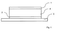
- an organic layer arrangement 4 is arranged between an electrode 1 and a counterelectrode 2, which is formed on a substrate 3, which in turn is in electrical contact with the electrode 1 and the counterelectrode 2.
- an electrical voltage can be applied to the organic layer arrangement 4.
- the application of the electrical voltage causes free charge carriers, namely electrons and holes, to migrate within the organic layer arrangement 4 to a light-emitting region and recombine there with the emission of light.
- ETL - electron transport layer HTL - hole transport layer
- EBL electron block layer HBL hole block layer
- EL light emitting region ETL - electron transport layer
- layers HBL and / or EBL may be omitted, for example, when layer EL is electron transporting / hole transporting.
- At least one pn / np junction is always formed, in which charge carriers are generated on application of an electrical voltage to the two electrodes, namely electrons and holes.
- the aforementioned embodiments for the organic layer arrangement 4 can also be combined with one another as desired, so that two transitions in the organic layer arrangement 4 can also be formed.
- one or more charge-generating regions or charge-generating layers are formed, for example: anode / n-doped ETL / EBL / EL / HBL / p-doped HTL / cathode or anode / n-doped ETL / p-doped HTL / EBL / EL / HBL / n-doped ETL / p-doped HTL / cathode.
- the energy difference between the lowest unoccupied molecular orbital (LUMO - "Lowest Unoccupied Molecular Orbital”) of the material of the n-type doped ETL and the highest occupied molecular orbital (HOMO - "Highest Occupied Molecular Orbital”) of the material the EBL is less than 1.5eV, preferably less than 1.0eV and more preferably less than 0.5eV.
- the energy difference between the HOMO of the material of the p-doped HTL and the LUMO of the material of the HBL is less than 1.5 eV, preferably less than 1.0 eV, and more preferably less than 0.5 eV.
- ITO - indium tin oxide; A1 - aluminum; STTB 2,7-tetra- (di-p-tolylamine) -9,9'-spirobifluorene; Pdop - 1,3,4,5,7,8-hexa-fluoronaphtho-2,6-quinone tetracyanoethane; NPB - N, N'-di (naphthalen-2-yl) -N, N'-diphenylbenzidine; Ndop - tetrakis (1,2,3,3a, 4,5,6,6a, 7,8-decahydro-1,9,9b-triazaphenalenyl) di-tertiary (II); ETM -2,4,7,9-tetraphenyl phenanthrolines: ORE - iridium (III) bis (2-methyl-benzo [f, h] quinoxalines) (acetylacetonates); H
- P-dop has a reduction potential of about + 0.2V vs. Fc / Fc + .
- NPB has an oxidation potential of about 0.3V vs. Fc / Fc + .
- Ndop has an oxidation potential of about -2.2V vs Fc / Fc + .
- ETM has a reduction potential of about -2.2V vs. Fc / Fc + .
- HTM has an oxidation potential of about 0.2 V vs. Fc / Fc + .
- Fullerene C60 has a reduction potential of about -1V.
- STTB has an oxidation potential of about 0.1V vs. Fc / Fc + .
- HAT has a reduction potential of about -0.6V vs. Fc / Fc + .
- p denotes a p-type layer
- i denotes an undoped layer (insulator)
- n denotes an n-type layer.
- Example 1 an organic electronic component having a conventional pin structure was produced as a reference.
- the device has the following layer structure: Substrate: Glass / anode: 90nm ITO / p-doped layer: 50nm Pdop in STTB (1.5wt%) / intrinsic layer: 10nm NPB / intrinsic EL: 20nm ORE in NPB (10%) / intrinsic interlayer: 10nm ETM / n-doped layer: 55nm Ndop in ETM (8wt%) / Cathode: 100nm Al.
- Example 2 an organic electronic device with an npin structure was fabricated: glass / anode: 90nm ITO / 45nm Ndop in ETM (8wt%) / 5nm Pdop in HTM (1.5wt%) / 10nm NPB / 20nm ORE in NPB ( 10%) / 10nm ETM / 55nm Ndop in ETM (8wt%) / 100nm Al.
- the conductivity of the layer of Ndop in ETM is about 2 * 10 -5 S / cm
- an organic electronic device with the following pinp layer structure was fabricated: glass / anode: 90nm ITO / 50nm Pdop in STTB (1.5wt%) / 10nm NPB / 20nm ORE in NPB (10%) / 10nm ETM / 55nm Ndop in ETM (8% by weight) / 5nm Pdop in HTM (1.5% by weight) / 100nm Al.
- the conductivity of the layer of Pdop in HTM is about 4 * 10 -5 S / cm
- Example 4 an organic electronic device with the following layer structure was prepared (npinp): glass / anode: 90nm ITO / 45nm Ndop in ETM (8wt%) / 5nm Pdop in HTM (1.5wt%) / 10nm NPB / 20nm ORE in NPB (10%) / 10nm ETM / 55nm Ndop in ETM (8wt%) / 5nm Pdop in HTM (1.5wt%) / 100nm Al.
- Example 5 glass / 90 nm ITO / 5 nm Pdop in HTM (1.5% by weight) / 45 nm Ndop in ETM (8% by weight) / 10 nm ETM / 20 nm ORE in NPB (10 %) / 10nm NPB / 5nm Pdop in HTM (1.5wt%) / 55nm Ndop in ETM (8wt%) / Anode: 100nm Al
- Example 6 an organic electronic device having a simplified structure was prepared as follows: Glass / Anode: ITO / 1,3,4,5,7,8-hexafluoronaphtho-2,6-quinone tetracyano-methane doped with Ndop (50nm) / NPD: ORE (20nm, 10% by weight) / BPhen (10nm) / BPhen: Cs (8: 1, 60nm) / Al. At an operating voltage of 2.8V, a current density of 10mA / cm 2 was measured. The electrical conductivity of the layer of 1,3,4,5,7,8-hexafluoronaphtho-2,6-quinonetetracyanomethane doped with Ndop is about g * 10 -5 S / cm
- Example 7 a structure was prepared for comparison: glass / anode: ITO / 1,3,4,5,7,8-hexafluoronaphtho-2,6-quinonetetracyanomethane (50nm) / NPD: ORE (20nm, 10% by weight) / BPhen (10nm) / BPhen: Cs (60nm) / Al. At an operating voltage of 3.3V, a current density of 10mA / cm 2 was measured.
- Example 8 an organic electronic device with a simplified structure was fabricated as follows: Glass / Anode: ITO / HAT doped with Ndop (50nm) / NPD: ORE (20nm, 10wt%) / BPhen (10nm) / BPhen: Cs (8 : 1, 60nm) / Al. At an operating voltage of 4.4V, a current density of 10mA / cm 2 was measured. The conductivity of the layer HAT doped with Ndop is about 5 * 10 -5 S / cm
- the layers 22 and 24 form a pn junction, wherein the layer 23 of gold is provided between the two layers as a stabilizing metal layer, which in turn is not closed.
- the electrical conductivity of the layer 22 was less than 0.5 S / cm.
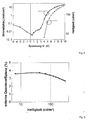
- FIGS. 5 and 6 show data for example 10.
- Examples 9 and 10 a doped layer of fullerene is used in each case.
- Fullerenes in particular the Buckminster fullerene C60, have been intensively researched since their discovery in 1985 and are used, for example, in organic solar cells as acceptor material (cf. US 6,580,027 B2 ).
- WO 92/04279 discloses a process for producing C60 and C70 in larger quantities.
- Fullerenes are now available as inexpensive starting materials.
- fullerene C60 doped with dopants exhibit conductivities greater than 2 S / cm.
- the layer formed from fullerene is preferably applied in a high vacuum by means of simultaneous evaporation of the fullerene and of the organic dopant, ie with the method customary for organic thin films.
- the application of such a fullerene layer adds without additional effort in the production process of the organic light-emitting component.
- an organic electronic device with the following layer structure was fabricated (nip): Cathode ITO / 75nm ETM doped with Ndop (9wt%) / 10nm ETM / 20nm BA1q doped with Ir (pic) 3 (10wt%) / 10nm NPB / 45nm STTB doped with Pdop (6 wt%) / Anode 100nm Al.
- the ITO cathode is located on a transparent glass substrate.
- Example 12 an organic electronic device having the following layer structure was fabricated (nipn): Cathode ITO / 75nm ETM doped with Ndop (9wt%) / 10nm ETM / 20nm BA1q doped with Ir (pic) 3 (10wt%) / 10nm NPB / 20nm STTB doped with Pdop (6wt%) / 25nm ETM doped with Ndop (9wt%) / Anode 100nm Al. Compared to Example 11, a low operating voltage and higher current efficiency were measured using a pn junction in conjunction with the anode.
- An organic electronic device was fabricated with the following layer structure: Anode: 90nm ITO / 50nm Pdop in STTB (1.5wt%) / 10nm NPB / 20nm ORE in NPB (10%) / 10nm ETM / 10nm Ndop in ETM (8wt%) / 5nm Pdop in HTM (1.5 Weight percent) / 40nm Pdop in STTB (1.5 weight percent) / 100nm Al.
- the p-type p-type layer is multilayered to improve the stability of the device.
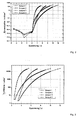
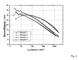
- FIG. 2 shows a graph of the current density as a function of the voltage for various embodiments of an organic component.
- FIG. 3 shows a graph of the luminance as a function of the voltage for the various embodiments of the organic electronic component.
Landscapes
- Physics & Mathematics (AREA)
- Engineering & Computer Science (AREA)
- Chemical & Material Sciences (AREA)
- Nanotechnology (AREA)
- Optics & Photonics (AREA)
- Mathematical Physics (AREA)
- Theoretical Computer Science (AREA)
- Crystallography & Structural Chemistry (AREA)
- Electroluminescent Light Sources (AREA)
- Led Devices (AREA)
Priority Applications (4)
| Application Number | Priority Date | Filing Date | Title |
|---|---|---|---|
| EP06026743A EP1808910B1 (fr) | 2006-01-11 | 2006-12-22 | Composant électronique doté dýau moins un dispositif de couche organique |
| US12/519,912 US20120025171A1 (en) | 2006-01-11 | 2007-12-21 | Electronic Component with at Least One Organic Layer Arrangement |
| JP2009541910A JP2010514174A (ja) | 2006-12-22 | 2007-12-21 | 少なくとも1つの有機層配列を有する電子素子 |
| PCT/EP2007/011353 WO2008077615A1 (fr) | 2006-12-22 | 2007-12-21 | Composant électronique avec au moins un agencement de couches organiques |
Applications Claiming Priority (2)
| Application Number | Priority Date | Filing Date | Title |
|---|---|---|---|
| EP06000436A EP1808909A1 (fr) | 2006-01-11 | 2006-01-11 | Dispositif électroluminescent |
| EP06026743A EP1808910B1 (fr) | 2006-01-11 | 2006-12-22 | Composant électronique doté dýau moins un dispositif de couche organique |
Publications (3)
| Publication Number | Publication Date |
|---|---|
| EP1808910A2 true EP1808910A2 (fr) | 2007-07-18 |
| EP1808910A3 EP1808910A3 (fr) | 2007-12-19 |
| EP1808910B1 EP1808910B1 (fr) | 2011-11-16 |
Family
ID=36572074
Family Applications (3)
| Application Number | Title | Priority Date | Filing Date |
|---|---|---|---|
| EP06000436A Withdrawn EP1808909A1 (fr) | 2006-01-11 | 2006-01-11 | Dispositif électroluminescent |
| EP06026743A Ceased EP1808910B1 (fr) | 2006-01-11 | 2006-12-22 | Composant électronique doté dýau moins un dispositif de couche organique |
| EP07711334.8A Not-in-force EP1982362B1 (fr) | 2006-01-11 | 2007-01-11 | Composant optoélectronique organique |
Family Applications Before (1)
| Application Number | Title | Priority Date | Filing Date |
|---|---|---|---|
| EP06000436A Withdrawn EP1808909A1 (fr) | 2006-01-11 | 2006-01-11 | Dispositif électroluminescent |
Family Applications After (1)
| Application Number | Title | Priority Date | Filing Date |
|---|---|---|---|
| EP07711334.8A Not-in-force EP1982362B1 (fr) | 2006-01-11 | 2007-01-11 | Composant optoélectronique organique |
Country Status (6)
| Country | Link |
|---|---|
| US (3) | US8084766B2 (fr) |
| EP (3) | EP1808909A1 (fr) |
| JP (1) | JP5302690B2 (fr) |
| CN (1) | CN101395734B (fr) |
| DE (1) | DE112007000135B4 (fr) |
| WO (2) | WO2007082674A2 (fr) |
Cited By (9)
| Publication number | Priority date | Publication date | Assignee | Title |
|---|---|---|---|---|
| DE102008058230A1 (de) | 2008-11-19 | 2010-05-20 | Novaled Ag | Chinoxalinverbindung, organische Leuchtdiode, organischer Dünnfilmtransistor und Solarzelle |
| WO2010057471A1 (fr) | 2008-11-19 | 2010-05-27 | Novaled Ag | Composés de chinoxaline et matériaux semi-conducteurs |
| EP2194055A1 (fr) | 2008-12-03 | 2010-06-09 | Novaled AG | Composants de pyridoquinazoline ou phénathronline pontés et matériau de semi-conducteur organique comportant ce composant |
| DE102008061843A1 (de) | 2008-12-15 | 2010-06-17 | Novaled Ag | Heterocyclische Verbindungen und deren Verwendung in elektronischen und optoelektronischen Bauelementen |
| EP2246862A1 (fr) | 2009-04-27 | 2010-11-03 | Novaled AG | Dispositif électronique organique comportant un matériau semi-conducteur organique |
| WO2011063927A1 (fr) | 2009-11-24 | 2011-06-03 | Novaled Ag | Dispositif électronique organique comprenant un matériau semi-conducteur organique |
| EP2452946A1 (fr) | 2010-11-16 | 2012-05-16 | Novaled AG | Oxides de pyridylphosphine pour dispositif électronique organique et dispositif électronique organique |
| EP2463927A1 (fr) | 2010-12-08 | 2012-06-13 | Novaled AG | Matériau pour dispositif électronique organique et dispositif électronique organique |
| WO2013135237A1 (fr) | 2012-03-15 | 2013-09-19 | Novaled Ag | Composés aromatiques amino-triphényles et utilisation desdits composés dans des composants semi-conducteurs organiques |
Families Citing this family (17)
| Publication number | Priority date | Publication date | Assignee | Title |
|---|---|---|---|---|
| WO2009139358A1 (fr) | 2008-05-16 | 2009-11-19 | Semiconductor Energy Laboratory Co., Ltd. | Dérivé de triarylamine, substance émettant de la lumière, élément émettant de la lumière, dispositif émettant de la lumière, et dispositif électronique |
| DE102008049057B4 (de) * | 2008-09-26 | 2019-01-31 | Fraunhofer-Gesellschaft zur Förderung der angewandten Forschung e.V. | Organisches opto-elektrisches Bauelement und ein Verfahren zur Herstellung eines organischen opto-elektrischen Bauelements |
| CN102201541B (zh) | 2010-03-23 | 2015-11-25 | 株式会社半导体能源研究所 | 发光元件、发光装置、电子设备及照明装置 |
| JP5986992B2 (ja) | 2010-06-14 | 2016-09-06 | ノヴァレッド ゲーエムベーハー | 有機発光素子 |
| WO2012070233A1 (fr) * | 2010-11-22 | 2012-05-31 | Idemitsu Kosan Co.,Ltd. | Dispositif électroluminescent organique |
| US8883323B2 (en) | 2010-11-22 | 2014-11-11 | Idemitsu Kosan Co., Ltd. | Organic electroluminescence device |
| US20120126205A1 (en) * | 2010-11-22 | 2012-05-24 | Idemitsu Kosan Co., Ltd. | Organic electroluminescence device |
| US9324950B2 (en) | 2010-11-22 | 2016-04-26 | Idemitsu Kosan Co., Ltd. | Organic electroluminescence device |
| CN104321896B (zh) | 2012-05-31 | 2017-07-14 | 乐金显示有限公司 | 堆叠式有机发光二极管 |
| US9281490B2 (en) | 2012-05-31 | 2016-03-08 | Lg Chem, Ltd. | Organic electroluminescent device |
| CN104335379B (zh) * | 2012-05-31 | 2016-12-21 | 乐金显示有限公司 | 有机电致发光器件、包含该有机电致发光器件的显示器和照明设备 |
| TWI599083B (zh) * | 2012-05-31 | 2017-09-11 | 樂金顯示科技股份有限公司 | 有機電致發光裝置 |
| KR20140055452A (ko) * | 2012-10-31 | 2014-05-09 | 삼성디스플레이 주식회사 | 유기 발광 소자 |
| JPWO2015001691A1 (ja) * | 2013-07-05 | 2017-02-23 | エイソンテクノロジー株式会社 | 有機エレクトロルミネッセント素子 |
| JP5946929B2 (ja) * | 2015-01-29 | 2016-07-06 | ユー・ディー・シー アイルランド リミテッド | 有機電界発光素子 |
| KR102323243B1 (ko) * | 2015-07-22 | 2021-11-08 | 삼성디스플레이 주식회사 | 유기 발광 소자 및 이를 포함하는 유기 발광 표시 장치 |
| DE102015114010A1 (de) * | 2015-08-24 | 2017-03-02 | Osram Opto Semiconductors Gmbh | Optoelektronisches Bauelement, Verfahren zur Herstellung eines optoelektronischen Bauelements und Verfahren zum Betrieb eines optoelektronischen Bauelements |
Family Cites Families (172)
| Publication number | Priority date | Publication date | Assignee | Title |
|---|---|---|---|---|
| US4356429A (en) | 1980-07-17 | 1982-10-26 | Eastman Kodak Company | Organic electroluminescent cell |
| US4769292A (en) | 1987-03-02 | 1988-09-06 | Eastman Kodak Company | Electroluminescent device with modified thin film luminescent zone |
| DE3804293A1 (de) | 1988-02-12 | 1989-08-24 | Philips Patentverwaltung | Anordnung mit einer elektrolumineszenz- oder laserdiode |
| JP2813428B2 (ja) | 1989-08-17 | 1998-10-22 | 三菱電機株式会社 | 電界効果トランジスタ及び該電界効果トランジスタを用いた液晶表示装置 |
| US7494638B1 (en) | 1990-08-30 | 2009-02-24 | Mitsubishi Corporation | Form of carbon |
| US5093698A (en) | 1991-02-12 | 1992-03-03 | Kabushiki Kaisha Toshiba | Organic electroluminescent device |
| US5150006A (en) * | 1991-08-01 | 1992-09-22 | Eastman Kodak Company | Blue emitting internal junction organic electroluminescent device (II) |
| EP0676461B1 (fr) | 1994-04-07 | 2002-08-14 | Covion Organic Semiconductors GmbH | Composés spiro et leur application comme matières électroluminescentes |
| US5707745A (en) | 1994-12-13 | 1998-01-13 | The Trustees Of Princeton University | Multicolor organic light emitting devices |
| US5703436A (en) | 1994-12-13 | 1997-12-30 | The Trustees Of Princeton University | Transparent contacts for organic devices |
| JP3586939B2 (ja) | 1994-12-22 | 2004-11-10 | 株式会社デンソー | El素子およびその製造方法 |
| WO1997020355A1 (fr) | 1995-11-28 | 1997-06-05 | International Business Machines Corporation | Alliages organiques/non-organiques utilises pour ameliorer des dispositifs electroluminescents organiques |
| DE19625622A1 (de) | 1996-06-26 | 1998-01-02 | Siemens Ag | Lichtabstrahlendes Halbleiterbauelement mit Lumineszenzkonversionselement |
| JPH10125469A (ja) | 1996-10-24 | 1998-05-15 | Tdk Corp | 有機el発光素子 |
| US5885498A (en) * | 1996-12-11 | 1999-03-23 | Matsushita Electric Industrial Co., Ltd. | Organic light emitting device and method for producing the same |
| US5811833A (en) | 1996-12-23 | 1998-09-22 | University Of So. Ca | Electron transporting and light emitting layers based on organic free radicals |
| US5917280A (en) | 1997-02-03 | 1999-06-29 | The Trustees Of Princeton University | Stacked organic light emitting devices |
| US6337492B1 (en) | 1997-07-11 | 2002-01-08 | Emagin Corporation | Serially-connected organic light emitting diode stack having conductors sandwiching each light emitting layer |
| JP3736071B2 (ja) | 1997-09-30 | 2006-01-18 | コニカミノルタホールディングス株式会社 | 有機エレクトロルミネセンス素子 |
| US6303238B1 (en) | 1997-12-01 | 2001-10-16 | The Trustees Of Princeton University | OLEDs doped with phosphorescent compounds |
| JP3203227B2 (ja) * | 1998-02-27 | 2001-08-27 | 三洋電機株式会社 | 表示装置の製造方法 |
| GB9805476D0 (en) | 1998-03-13 | 1998-05-13 | Cambridge Display Tech Ltd | Electroluminescent devices |
| JP2991183B2 (ja) * | 1998-03-27 | 1999-12-20 | 日本電気株式会社 | 有機エレクトロルミネッセンス素子 |
| WO1999052992A1 (fr) | 1998-04-09 | 1999-10-21 | Idemitsu Kosan Co., Ltd. | Dispositif electroluminescent organique |
| JP3884564B2 (ja) | 1998-05-20 | 2007-02-21 | 出光興産株式会社 | 有機el発光素子およびそれを用いた発光装置 |
| US6437769B1 (en) | 1998-07-24 | 2002-08-20 | Seiko Epson Corporation | Display apparatus |
| DE19836943B9 (de) | 1998-08-17 | 2008-01-31 | Osram Opto Semiconductors Gmbh | Photolumineszenzschicht im optischen und angrenzenden Spektralbereichen |
| JP2000075836A (ja) * | 1998-09-02 | 2000-03-14 | Sharp Corp | 有機el発光装置とその駆動方法 |
| US6274980B1 (en) | 1998-11-16 | 2001-08-14 | The Trustees Of Princeton University | Single-color stacked organic light emitting device |
| JP2000196140A (ja) | 1998-12-28 | 2000-07-14 | Sharp Corp | 有機エレクトロルミネッセンス素子とその製造法 |
| JP2000231992A (ja) | 1999-02-09 | 2000-08-22 | Stanley Electric Co Ltd | 面光源装置 |
| GB2347013A (en) | 1999-02-16 | 2000-08-23 | Sharp Kk | Charge-transport structures |
| US7001536B2 (en) | 1999-03-23 | 2006-02-21 | The Trustees Of Princeton University | Organometallic complexes as phosphorescent emitters in organic LEDs |
| DE19916745A1 (de) | 1999-04-13 | 2000-10-19 | Mannesmann Vdo Ag | Lichtemittierende Diode mit organischen lichtemittierenden Stoffen zur Erzeugung von Licht mit Mischfarben |
| WO2000076008A1 (fr) | 1999-06-09 | 2000-12-14 | Cambridge Display Technology Limited | Realisation de dispositifs electroluminescents organiques |
| US6579422B1 (en) | 1999-07-07 | 2003-06-17 | Sony Corporation | Method and apparatus for manufacturing flexible organic EL display |
| US6310360B1 (en) * | 1999-07-21 | 2001-10-30 | The Trustees Of Princeton University | Intersystem crossing agents for efficient utilization of excitons in organic light emitting devices |
| BE1012802A3 (fr) | 1999-07-28 | 2001-03-06 | Cockerill Rech & Dev | Dispositif electroluminescent et son procede de fabrication. |
| JP2001148292A (ja) * | 1999-09-08 | 2001-05-29 | Denso Corp | 有機el素子 |
| TW474114B (en) | 1999-09-29 | 2002-01-21 | Junji Kido | Organic electroluminescent device, organic electroluminescent device assembly and method of controlling the emission spectrum in the device |
| US7560175B2 (en) | 1999-12-31 | 2009-07-14 | Lg Chem, Ltd. | Electroluminescent devices with low work function anode |
| KR100377321B1 (ko) | 1999-12-31 | 2003-03-26 | 주식회사 엘지화학 | 피-형 반도체 성질을 갖는 유기 화합물을 포함하는 전기소자 |
| US6639357B1 (en) * | 2000-02-28 | 2003-10-28 | The Trustees Of Princeton University | High efficiency transparent organic light emitting devices |
| US7233026B2 (en) * | 2000-03-23 | 2007-06-19 | Emagin Corporation | Light extraction from color changing medium layers in organic light emitting diode devices |
| US6660410B2 (en) | 2000-03-27 | 2003-12-09 | Idemitsu Kosan Co., Ltd. | Organic electroluminescence element |
| JP4094203B2 (ja) | 2000-03-30 | 2008-06-04 | 出光興産株式会社 | 有機エレクトロルミネッセンス素子及び有機発光媒体 |
| US6777871B2 (en) * | 2000-03-31 | 2004-08-17 | General Electric Company | Organic electroluminescent devices with enhanced light extraction |
| GB2361355B (en) * | 2000-04-14 | 2004-06-23 | Seiko Epson Corp | Light emitting device |
| GB2361356B (en) | 2000-04-14 | 2005-01-05 | Seiko Epson Corp | Light emitting device |
| US7525165B2 (en) * | 2000-04-17 | 2009-04-28 | Semiconductor Energy Laboratory Co., Ltd. | Light emitting device and manufacturing method thereof |
| TW516164B (en) * | 2000-04-21 | 2003-01-01 | Semiconductor Energy Lab | Self-light emitting device and electrical appliance using the same |
| US6645645B1 (en) | 2000-05-30 | 2003-11-11 | The Trustees Of Princeton University | Phosphorescent organic light emitting devices |
| TWI251089B (en) * | 2000-06-19 | 2006-03-11 | Nitto Denko Corp | Polarizer, polarizing plate, and liquid crystal display using the same |
| US6956324B2 (en) | 2000-08-04 | 2005-10-18 | Semiconductor Energy Laboratory Co., Ltd. | Semiconductor device and manufacturing method therefor |
| JP2002082627A (ja) | 2000-09-07 | 2002-03-22 | Sony Corp | 表示装置 |
| TW527848B (en) | 2000-10-25 | 2003-04-11 | Matsushita Electric Industrial Co Ltd | Light-emitting element and display device and lighting device utilizing thereof |
| KR20030072349A (ko) | 2000-11-02 | 2003-09-13 | 쓰리엠 이노베이티브 프로퍼티즈 컴파니 | 방사 디스플레이의 휘도 증대 |
| DE10058578C2 (de) | 2000-11-20 | 2002-11-28 | Univ Dresden Tech | Lichtemittierendes Bauelement mit organischen Schichten |
| US6573651B2 (en) | 2000-12-18 | 2003-06-03 | The Trustees Of Princeton University | Highly efficient OLEDs using doped ambipolar conductive molecular organic thin films |
| JP4220669B2 (ja) | 2000-12-26 | 2009-02-04 | 出光興産株式会社 | 有機エレクトロルミネッセンス素子 |
| TW519770B (en) | 2001-01-18 | 2003-02-01 | Semiconductor Energy Lab | Light emitting device and manufacturing method thereof |
| SG107573A1 (en) | 2001-01-29 | 2004-12-29 | Semiconductor Energy Lab | Light emitting device |
| KR100898304B1 (ko) | 2001-03-02 | 2009-05-19 | 더 트러스티즈 오브 프린스턴 유니버시티 | 이중 도우프층, 인광 유기 발광 디바이스 |
| JP4234998B2 (ja) | 2001-03-29 | 2009-03-04 | 富士フイルム株式会社 | エレクトロルミネッセンス素子 |
| US6933673B2 (en) * | 2001-04-27 | 2005-08-23 | Semiconductor Energy Laboratory Co., Ltd. | Luminescent device and process of manufacturing the same |
| JP2003017276A (ja) * | 2001-04-27 | 2003-01-17 | Semiconductor Energy Lab Co Ltd | 発光装置及びその作製方法 |
| US6580027B2 (en) | 2001-06-11 | 2003-06-17 | Trustees Of Princeton University | Solar cells using fullerenes |
| US6784016B2 (en) | 2001-06-21 | 2004-08-31 | The Trustees Of Princeton University | Organic light-emitting devices with blocking and transport layers |
| JP4152665B2 (ja) * | 2001-07-11 | 2008-09-17 | 株式会社半導体エネルギー研究所 | 発光装置及びその作製方法 |
| DE10135513B4 (de) | 2001-07-20 | 2005-02-24 | Novaled Gmbh | Lichtemittierendes Bauelement mit organischen Schichten |
| JP2003043998A (ja) | 2001-07-30 | 2003-02-14 | Pioneer Electronic Corp | ディスプレイ装置 |
| KR100439648B1 (ko) | 2001-08-29 | 2004-07-12 | 엘지.필립스 엘시디 주식회사 | 유기전계발광소자 |
| US6734038B2 (en) | 2001-09-04 | 2004-05-11 | The Trustees Of Princeton University | Method of manufacturing high-mobility organic thin films using organic vapor phase deposition |
| WO2003023876A1 (fr) * | 2001-09-05 | 2003-03-20 | Sharp Kabushiki Kaisha | Structure polymere, element fonctionnel comportant une telle structure ; transistor et ecran presentant cette structure |
| DE10145492B4 (de) | 2001-09-14 | 2004-11-11 | Novaled Gmbh | Elektrolumineszente Lichtemissionseinrichtung, insbesondere als Weißlichtquelle |
| US6680578B2 (en) | 2001-09-19 | 2004-01-20 | Osram Opto Semiconductors, Gmbh | Organic light emitting diode light source |
| KR100437886B1 (ko) * | 2001-09-25 | 2004-06-30 | 한국과학기술원 | 고발광효율 광결정 유기발광소자 |
| US6620350B2 (en) * | 2001-10-01 | 2003-09-16 | Hon Hai Precision Ind. Co., Ltd. | Method for making gradient refractive index optical components |
| JP2003203769A (ja) | 2001-10-29 | 2003-07-18 | Sony Corp | 線状パターン及びパターン形成方法、画像表示装置及びその製造方法 |
| AU2002366136A1 (en) | 2001-11-22 | 2003-06-10 | Canon Kabushiki Kaisha | Light-emitting element, production method thereof, and light-emitting apparatus |
| JP3852916B2 (ja) | 2001-11-27 | 2006-12-06 | パイオニア株式会社 | ディスプレイ装置 |
| US6734457B2 (en) * | 2001-11-27 | 2004-05-11 | Semiconductor Energy Laboratory Co., Ltd. | Light emitting device |
| DE10157945C2 (de) * | 2001-11-27 | 2003-09-18 | Osram Opto Semiconductors Gmbh | Verfahren zur Herstellung eines organischen, elektrolumineszierenden Displays sowie ein organisches, elektrolumineszierendes Display |
| US7141817B2 (en) * | 2001-11-30 | 2006-11-28 | Semiconductor Energy Laboratory Co., Ltd. | Light emitting device |
| US6903505B2 (en) * | 2001-12-17 | 2005-06-07 | General Electric Company | Light-emitting device with organic electroluminescent material and photoluminescent materials |
| DE10164016B4 (de) * | 2001-12-28 | 2020-01-23 | Osram Opto Semiconductors Gmbh | Organische Leuchtdiode (OLED) und Verfahren zu ihrer Herstellung |
| US7012363B2 (en) * | 2002-01-10 | 2006-03-14 | Universal Display Corporation | OLEDs having increased external electroluminescence quantum efficiencies |
| US6872472B2 (en) | 2002-02-15 | 2005-03-29 | Eastman Kodak Company | Providing an organic electroluminescent device having stacked electroluminescent units |
| DE10207859A1 (de) | 2002-02-20 | 2003-09-04 | Univ Dresden Tech | Dotiertes organisches Halbleitermaterial sowie Verfahren zu dessen Herstellung |
| US6833667B2 (en) * | 2002-02-27 | 2004-12-21 | Matsushita Electric Industrial Co., Ltd. | Organic electroluminescence element and image forming apparatus or portable terminal unit using thereof |
| DE10209789A1 (de) * | 2002-02-28 | 2003-09-25 | Univ Dresden Tech | Photoaktives Bauelement mit organischen Schichten |
| JP3933591B2 (ja) | 2002-03-26 | 2007-06-20 | 淳二 城戸 | 有機エレクトロルミネッセント素子 |
| DE10215210B4 (de) * | 2002-03-28 | 2006-07-13 | Novaled Gmbh | Transparentes, thermisch stabiles lichtemittierendes Bauelement mit organischen Schichten |
| JP2003297561A (ja) | 2002-03-29 | 2003-10-17 | Fuji Photo Film Co Ltd | 有機薄膜素子の製造方法及び有機薄膜素子 |
| GB0208506D0 (en) | 2002-04-12 | 2002-05-22 | Dupont Teijin Films Us Ltd | Film coating |
| GB2388236A (en) | 2002-05-01 | 2003-11-05 | Cambridge Display Tech Ltd | Display and driver circuits |
| CN1666579A (zh) * | 2002-05-08 | 2005-09-07 | 泽奥勒克斯公司 | 使用反馈增强型发光二极管的照明器件 |
| DE10224021B4 (de) | 2002-05-24 | 2006-06-01 | Novaled Gmbh | Phosphoreszentes lichtemittierendes Bauelement mit organischen Schichten |
| US20030230980A1 (en) | 2002-06-18 | 2003-12-18 | Forrest Stephen R | Very low voltage, high efficiency phosphorescent oled in a p-i-n structure |
| US6670772B1 (en) | 2002-06-27 | 2003-12-30 | Eastman Kodak Company | Organic light emitting diode display with surface plasmon outcoupling |
| DE10229231B9 (de) | 2002-06-28 | 2006-05-11 | Osram Opto Semiconductors Gmbh | Verfahren zum Herstellen eines Strahlung emittierenden und/oder empfangenden Halbleiterchips mit einer Strahlungsein- und/oder -auskoppel-Mikrostruktur |
| GB0215309D0 (en) | 2002-07-03 | 2002-08-14 | Cambridge Display Tech Ltd | Combined information display and information input device |
| US6642092B1 (en) | 2002-07-11 | 2003-11-04 | Sharp Laboratories Of America, Inc. | Thin-film transistors formed on a metal foil substrate |
| DE10232238A1 (de) | 2002-07-17 | 2004-02-05 | Philips Intellectual Property & Standards Gmbh | Elektrolumineszierende Vorrichtung aus zweidimensionalem Array |
| US20050270279A1 (en) | 2002-07-23 | 2005-12-08 | Koninklijke Philips Electronics N.V. | Electroluminescent display and electronic device comprising such a display |
| GB2392023A (en) | 2002-08-05 | 2004-02-18 | Gen Electric | Series connected oled structure and fabrication method |
| US7034470B2 (en) | 2002-08-07 | 2006-04-25 | Eastman Kodak Company | Serially connecting OLED devices for area illumination |
| TW556446B (en) | 2002-09-11 | 2003-10-01 | Opto Tech Corp | Organic light-emitting device and the manufacturing method thereof |
| US20040067324A1 (en) * | 2002-09-13 | 2004-04-08 | Lazarev Pavel I | Organic photosensitive optoelectronic device |
| JP4288918B2 (ja) | 2002-09-26 | 2009-07-01 | セイコーエプソン株式会社 | 有機elパネルおよびその製造方法、それを用いた電気光学パネル並びに電子機器 |
| KR20050072424A (ko) * | 2002-10-01 | 2005-07-11 | 코닌클리케 필립스 일렉트로닉스 엔.브이. | 광 출력이 향상된 전기발광 디스플레이 |
| US6965197B2 (en) | 2002-10-01 | 2005-11-15 | Eastman Kodak Company | Organic light-emitting device having enhanced light extraction efficiency |
| US6717358B1 (en) * | 2002-10-09 | 2004-04-06 | Eastman Kodak Company | Cascaded organic electroluminescent devices with improved voltage stability |
| US7224532B2 (en) * | 2002-12-06 | 2007-05-29 | Chevron U.S.A. Inc. | Optical uses diamondoid-containing materials |
| JP2004207065A (ja) * | 2002-12-25 | 2004-07-22 | Fuji Electric Holdings Co Ltd | 色変換発光デバイスおよびその製造方法ならびに該デバイスを用いるディスプレイ |
| JP2004207136A (ja) * | 2002-12-26 | 2004-07-22 | Nitto Denko Corp | 面光源及びこれを用いた表示装置 |
| JP2004214120A (ja) | 2003-01-08 | 2004-07-29 | Sony Corp | 有機電界発光素子の製造装置及び製造方法 |
| JP2004234942A (ja) | 2003-01-29 | 2004-08-19 | Yodogawa Steel Works Ltd | 無機el素子の作製方法 |
| KR100560785B1 (ko) | 2003-02-03 | 2006-03-13 | 삼성에스디아이 주식회사 | 저전압에서 구동되는 유기 전계 발광 소자 |
| JP3910926B2 (ja) * | 2003-02-26 | 2007-04-25 | 株式会社東芝 | 表示装置用透明基板の製造方法 |
| US6870196B2 (en) | 2003-03-19 | 2005-03-22 | Eastman Kodak Company | Series/parallel OLED light source |
| EP1606846B1 (fr) | 2003-03-24 | 2010-10-27 | Konarka Technologies, Inc. | Cellule photovoltaique a electrode a mailles |
| US7521113B2 (en) | 2003-04-28 | 2009-04-21 | Zheng-Hong Lu | Light-emitting devices with fullerene layer |
| US6936961B2 (en) | 2003-05-13 | 2005-08-30 | Eastman Kodak Company | Cascaded organic electroluminescent device having connecting units with N-type and P-type organic layers |
| EP1477892B1 (fr) | 2003-05-16 | 2015-12-23 | Sap Se | Système, procédé, programme informatique et article de fabrication pour entrer des données dans un système informatique |
| CN100477873C (zh) | 2003-07-10 | 2009-04-08 | 理想星株式会社 | 发光元件及发光装置 |
| US6885025B2 (en) * | 2003-07-10 | 2005-04-26 | Universal Display Corporation | Organic light emitting device structures for obtaining chromaticity stability |
| JP4194436B2 (ja) | 2003-07-14 | 2008-12-10 | キヤノン株式会社 | 電界効果型有機トランジスタ |
| DE10335727A1 (de) | 2003-08-05 | 2005-02-24 | H.C. Starck Gmbh | Transparente Elektrode für elektro-optische Aufbauten |
| US20060232992A1 (en) | 2003-08-12 | 2006-10-19 | Koninklijke Philips Electronics N.V. | Circuit arrangement for ac driving of organic diodes |
| JP2005063840A (ja) | 2003-08-13 | 2005-03-10 | Toshiba Matsushita Display Technology Co Ltd | 自発光表示装置及び有機el表示装置 |
| DE10338406A1 (de) | 2003-08-18 | 2005-03-24 | Novaled Gmbh | Dotierte organische Halbleitermaterialien sowie Verfahren zu deren Herstellung |
| US7180089B2 (en) | 2003-08-19 | 2007-02-20 | National Taiwan University | Reconfigurable organic light-emitting device and display apparatus employing the same |
| DE10339772B4 (de) | 2003-08-27 | 2006-07-13 | Novaled Gmbh | Licht emittierendes Bauelement und Verfahren zu seiner Herstellung |
| JP2005116193A (ja) | 2003-10-02 | 2005-04-28 | Toyota Industries Corp | 有機電界発光素子及び当該素子を備えた有機電界発光デバイス |
| DE10347856B8 (de) | 2003-10-10 | 2006-10-19 | Colorado State University Research Foundation, Fort Collins | Halbleiterdotierung |
| US7432124B2 (en) | 2003-11-04 | 2008-10-07 | 3M Innovative Properties Company | Method of making an organic light emitting device |
| JP4243237B2 (ja) | 2003-11-10 | 2009-03-25 | 淳二 城戸 | 有機素子、有機el素子、有機太陽電池、及び、有機fet構造、並びに、有機素子の製造方法 |
| JP2005156925A (ja) | 2003-11-26 | 2005-06-16 | Hitachi Displays Ltd | 表示装置 |
| DE10357044A1 (de) | 2003-12-04 | 2005-07-14 | Novaled Gmbh | Verfahren zur Dotierung von organischen Halbleitern mit Chinondiiminderivaten |
| KR20050066970A (ko) * | 2003-12-26 | 2005-06-30 | 닛토덴코 가부시키가이샤 | 전자발광 장치, 이를 사용하는 면광원 및 디스플레이 |
| US7030554B2 (en) | 2004-02-06 | 2006-04-18 | Eastman Kodak Company | Full-color organic display having improved blue emission |
| JP4276109B2 (ja) | 2004-03-01 | 2009-06-10 | ローム株式会社 | 有機エレクトロルミネッセント素子 |
| DE102004010954A1 (de) | 2004-03-03 | 2005-10-06 | Novaled Gmbh | Verwendung eines Metallkomplexes als n-Dotand für ein organisches halbleitendes Matrixmaterial, organisches Halbleitermaterial und elektronisches Bauteil |
| CN1961613B (zh) * | 2004-03-26 | 2011-06-29 | 松下电工株式会社 | 有机发光器件 |
| CN100508238C (zh) | 2004-05-11 | 2009-07-01 | Lg化学株式会社 | 有机电子器件 |
| US20050269943A1 (en) | 2004-06-04 | 2005-12-08 | Michael Hack | Protected organic electronic devices and methods for making the same |
| US20060014044A1 (en) | 2004-07-14 | 2006-01-19 | Au Optronics Corporation | Organic light-emitting display with multiple light-emitting modules |
| DE102004035965B4 (de) * | 2004-07-23 | 2007-07-26 | Novaled Ag | Top-emittierendes, elektrolumineszierendes Bauelement mit zumindest einer organischen Schicht |
| EP1624502B1 (fr) * | 2004-08-04 | 2015-11-18 | Semiconductor Energy Laboratory Co., Ltd. | Dispositif électroluminescent, dispositif d'affichage et appareil électronique |
| WO2006015567A1 (fr) | 2004-08-13 | 2006-02-16 | Novaled Ag | Ensemble de couches pour un composant émetteur de lumière |
| CN1738069A (zh) | 2004-08-17 | 2006-02-22 | 国际商业机器公司 | 其电极具有增强注入特性的电子器件制造方法和电子器件 |
| US7273663B2 (en) * | 2004-08-20 | 2007-09-25 | Eastman Kodak Company | White OLED having multiple white electroluminescence units |
| DE102004041371B4 (de) | 2004-08-25 | 2007-08-02 | Novaled Ag | Bauelement auf Basis einer organischen Leuchtdiodeneinrichtung und Verfahren zur Herstellung |
| KR20060026776A (ko) | 2004-09-21 | 2006-03-24 | 삼성에스디아이 주식회사 | 유기 전계 발광 소자 및 그의 제조 방법 |
| JP4877874B2 (ja) | 2004-11-05 | 2012-02-15 | 株式会社半導体エネルギー研究所 | 発光素子、発光装置、電子機器及び照明機器 |
| US20060105200A1 (en) | 2004-11-17 | 2006-05-18 | Dmytro Poplavskyy | Organic electroluminescent device |
| US7321133B2 (en) * | 2004-11-17 | 2008-01-22 | Plextronics, Inc. | Heteroatomic regioregular poly(3-substitutedthiophenes) as thin film conductors in diodes which are not light emitting or photovoltaic |
| US7279705B2 (en) * | 2005-01-14 | 2007-10-09 | Au Optronics Corp. | Organic light-emitting device |
| EP1684365A3 (fr) | 2005-01-20 | 2008-08-13 | Fuji Electric Holdings Co., Ltd. | Transistor |
| KR101097301B1 (ko) * | 2005-02-05 | 2011-12-23 | 삼성모바일디스플레이주식회사 | 백색발광소자 |
| DE102005010978A1 (de) * | 2005-03-04 | 2006-09-07 | Technische Universität Dresden | Photoaktives Bauelement mit organischen Schichten |
| ATE381117T1 (de) | 2005-04-13 | 2007-12-15 | Novaled Ag | Anordnung für eine organische leuchtdiode vom pin-typ und verfahren zum herstellen |
| US7629741B2 (en) * | 2005-05-06 | 2009-12-08 | Eastman Kodak Company | OLED electron-injecting layer |
| EP1729346A1 (fr) | 2005-06-01 | 2006-12-06 | Novaled AG | Dispositif électroluminescent comprenant un arrangement d'électrodes |
| JP4890117B2 (ja) | 2005-06-30 | 2012-03-07 | 株式会社半導体エネルギー研究所 | 発光装置及びその作製方法 |
| EP1739765A1 (fr) | 2005-07-01 | 2007-01-03 | Novaled AG | Diode organoluminescent et empilement des OLEDs |
| DE502005005126D1 (de) * | 2005-08-11 | 2008-10-02 | Novaled Ag | Verfahren zum Herstellen eines top-emittierenden Bauteils sowie Verwendung |
| DE502005004675D1 (de) | 2005-12-21 | 2008-08-21 | Novaled Ag | Organisches Bauelement |
| EP1804308B1 (fr) | 2005-12-23 | 2012-04-04 | Novaled AG | Dispositif organique émetteur de lumière ayant plusieurs unités électroluminescentes organiques empilées les unes sur les autres |
| CN101165937A (zh) * | 2006-10-18 | 2008-04-23 | 清华大学 | 有机复合物p-n结及其制备方法以及应用该p-n结的有机复合物二极管 |
| DE102006059509B4 (de) | 2006-12-14 | 2012-05-03 | Novaled Ag | Organisches Leuchtbauelement |
-
2006
- 2006-01-11 EP EP06000436A patent/EP1808909A1/fr not_active Withdrawn
- 2006-12-22 EP EP06026743A patent/EP1808910B1/fr not_active Ceased
-
2007
- 2007-01-11 DE DE112007000135.6T patent/DE112007000135B4/de not_active Expired - Fee Related
- 2007-01-11 WO PCT/EP2007/000211 patent/WO2007082674A2/fr not_active Ceased
- 2007-01-11 CN CN2007800078593A patent/CN101395734B/zh not_active Expired - Fee Related
- 2007-01-11 EP EP07711334.8A patent/EP1982362B1/fr not_active Not-in-force
- 2007-01-11 JP JP2008549831A patent/JP5302690B2/ja not_active Expired - Fee Related
- 2007-01-11 US US12/160,344 patent/US8084766B2/en active Active
- 2007-01-11 WO PCT/EP2007/000208 patent/WO2007082673A2/fr not_active Ceased
- 2007-01-11 US US12/160,503 patent/US8502200B2/en not_active Expired - Fee Related
- 2007-12-21 US US12/519,912 patent/US20120025171A1/en not_active Abandoned
Non-Patent Citations (2)
| Title |
|---|
| TSUZUKI ET AL.: "Solar Energy Materials and Solar Cells", vol. 61, 15 February 2000, ELSEVIER SCIENCE PUBLISHERS, article "The effect of fullerene doping on photoelectric conversion using titanyl phthalocyanine and a perylene pigment", pages: 1 - 8 |
| VON SIGNERSKI ET AL.: "Journal of Non-Crystalline Solids", vol. 352, 1 November 2006, NORTH-HOLLAND PHYSICS PUBLISHING, article "The photovoltaic effect in a heterojunction of molybdenyl phthalocyanine and perylene dye", pages: 4319 - 4324 |
Cited By (11)
| Publication number | Priority date | Publication date | Assignee | Title |
|---|---|---|---|---|
| DE102008058230A1 (de) | 2008-11-19 | 2010-05-20 | Novaled Ag | Chinoxalinverbindung, organische Leuchtdiode, organischer Dünnfilmtransistor und Solarzelle |
| WO2010057471A1 (fr) | 2008-11-19 | 2010-05-27 | Novaled Ag | Composés de chinoxaline et matériaux semi-conducteurs |
| EP2194055A1 (fr) | 2008-12-03 | 2010-06-09 | Novaled AG | Composants de pyridoquinazoline ou phénathronline pontés et matériau de semi-conducteur organique comportant ce composant |
| US8475686B2 (en) | 2008-12-03 | 2013-07-02 | Novaled Ag | Bridged pyridoquinazoline or phenanthroline compounds and organic semiconducting material comprising that compound |
| DE102008061843A1 (de) | 2008-12-15 | 2010-06-17 | Novaled Ag | Heterocyclische Verbindungen und deren Verwendung in elektronischen und optoelektronischen Bauelementen |
| WO2010075836A2 (fr) | 2008-12-15 | 2010-07-08 | Novaled Ag | Composés hétérocycliques et leur utilisation dans des composants électroniques et optoélectroniques |
| EP2246862A1 (fr) | 2009-04-27 | 2010-11-03 | Novaled AG | Dispositif électronique organique comportant un matériau semi-conducteur organique |
| WO2011063927A1 (fr) | 2009-11-24 | 2011-06-03 | Novaled Ag | Dispositif électronique organique comprenant un matériau semi-conducteur organique |
| EP2452946A1 (fr) | 2010-11-16 | 2012-05-16 | Novaled AG | Oxides de pyridylphosphine pour dispositif électronique organique et dispositif électronique organique |
| EP2463927A1 (fr) | 2010-12-08 | 2012-06-13 | Novaled AG | Matériau pour dispositif électronique organique et dispositif électronique organique |
| WO2013135237A1 (fr) | 2012-03-15 | 2013-09-19 | Novaled Ag | Composés aromatiques amino-triphényles et utilisation desdits composés dans des composants semi-conducteurs organiques |
Also Published As
| Publication number | Publication date |
|---|---|
| DE112007000135A5 (de) | 2008-11-20 |
| DE112007000135B4 (de) | 2019-07-11 |
| US20120025171A1 (en) | 2012-02-02 |
| US20110186864A1 (en) | 2011-08-04 |
| JP5302690B2 (ja) | 2013-10-02 |
| EP1808909A1 (fr) | 2007-07-18 |
| EP1808910A3 (fr) | 2007-12-19 |
| CN101395734B (zh) | 2010-06-23 |
| EP1808910B1 (fr) | 2011-11-16 |
| EP1982362B1 (fr) | 2017-03-08 |
| WO2007082673A2 (fr) | 2007-07-26 |
| WO2007082673A3 (fr) | 2007-10-04 |
| WO2007082674A2 (fr) | 2007-07-26 |
| WO2007082674A3 (fr) | 2008-01-24 |
| US20100289007A1 (en) | 2010-11-18 |
| CN101395734A (zh) | 2009-03-25 |
| EP1982362A2 (fr) | 2008-10-22 |
| US8502200B2 (en) | 2013-08-06 |
| US8084766B2 (en) | 2011-12-27 |
| JP2009523304A (ja) | 2009-06-18 |
Similar Documents
| Publication | Publication Date | Title |
|---|---|---|
| EP1808910B1 (fr) | Composant électronique doté dýau moins un dispositif de couche organique | |
| WO2008077615A1 (fr) | Composant électronique avec au moins un agencement de couches organiques | |
| EP1336208B1 (fr) | Composant luminescent comportant des couches organiques | |
| EP2284923B1 (fr) | Agencement pour une diode luminescente organique de type PIN et son procédé de fabrication | |
| DE102013017361B4 (de) | Organisches Licht emittierendes Bauelement und Verfahren zur Herstellung eines organischen Licht ermittierenden Bauelements | |
| EP1806795B1 (fr) | Dispositif organique | |
| WO2011134458A1 (fr) | Matériau semi-conducteur organique et composant électronique | |
| EP2229699B1 (fr) | Complexes de dithiolène-métaux de transition, et composants électroniques ou optoélectroniques | |
| WO2013139660A1 (fr) | Composant optoélectronique et procédé de fabrication d'un composant optoélectronique | |
| DE102013107113B4 (de) | Organisches Licht emittierendes Bauelement und Verfahren zur Herstellung eines organischen Licht emittierenden Bauelements | |
| WO2015007920A1 (fr) | Procédé de production d'un composant optoélectronique et composant optoélectronique | |
| DE102009013685B4 (de) | Verwendung einer organischen Diode als organische Zenerdiode und Verfahren zum Betreiben | |
| WO2007121877A1 (fr) | Composant émetteur de lumière | |
| EP2659529B2 (fr) | Composant optoélectronique à couches dopées | |
| DE102012208235B4 (de) | Optoelektronisches Bauelement und Verfahren zum Herstellen eines optoelektronischen Bauelements | |
| WO2011044867A2 (fr) | Composant semiconducteur organique optoélectronique et procédé de production | |
| WO2005106987A1 (fr) | Systeme de couches pour diode luminescente organique | |
| WO2010057471A1 (fr) | Composés de chinoxaline et matériaux semi-conducteurs | |
| WO2017194213A1 (fr) | Couche organique conductrice d'électrons à dopage n | |
| DE102015102371B4 (de) | Organisches Licht emittierendes Bauelement | |
| DE102008058230B4 (de) | Chinoxalinverbindung, organische Leuchtdiode, organischer Dünnfilmtransistor und Solarzelle | |
| DE102012025879B3 (de) | Optoelektronisches Bauelement und Verfahren zum Herstellen eines optoelektronischen Bauelements | |
| DE102015104314A1 (de) | Verfahren zur Herstellung einer organischen Ladungsträgererzeugungsschicht und eines organischen Licht emittierenden Bauelements mit einer organischen Ladungsträgererzeugungsschicht | |
| WO2016180815A1 (fr) | Procédé de fabrication d'une couche de génération de porteurs de charge, procédé de fabrication d'un composant électroluminescent organique avec une couche de génération de porteurs de charge, et composant électroluminescent organique avec une couche de génération de porteurs de charge |
Legal Events
| Date | Code | Title | Description |
|---|---|---|---|
| PUAI | Public reference made under article 153(3) epc to a published international application that has entered the european phase |
Free format text: ORIGINAL CODE: 0009012 |
|
| AK | Designated contracting states |
Kind code of ref document: A2 Designated state(s): AT BE BG CH CY CZ DE DK EE ES FI FR GB GR HU IE IS IT LI LT LU LV MC NL PL PT RO SE SI SK TR |
|
| AX | Request for extension of the european patent |
Extension state: AL BA HR MK YU |
|
| PUAL | Search report despatched |
Free format text: ORIGINAL CODE: 0009013 |
|
| RIN1 | Information on inventor provided before grant (corrected) |
Inventor name: WALZER, KARSTEN Inventor name: ANSGAR, WERNER Inventor name: WELLMANN, PHILIPP Inventor name: CANZLER, TOBIAS DR. Inventor name: HARADA, KENTARO Inventor name: SCHWARTZ, GEORG Inventor name: PFEIFFER, MARTIN Inventor name: ZEIKA, OLAF |
|
| AK | Designated contracting states |
Kind code of ref document: A3 Designated state(s): AT BE BG CH CY CZ DE DK EE ES FI FR GB GR HU IE IS IT LI LT LU LV MC NL PL PT RO SE SI SK TR |
|
| AX | Request for extension of the european patent |
Extension state: AL BA HR MK YU |
|
| RIC1 | Information provided on ipc code assigned before grant |
Ipc: H01L 51/44 20060101ALI20071112BHEP Ipc: H01L 51/52 20060101AFI20070404BHEP |
|
| 17P | Request for examination filed |
Effective date: 20080331 |
|
| AKX | Designation fees paid |
Designated state(s): DE FR GB |
|
| 17Q | First examination report despatched |
Effective date: 20080811 |
|
| GRAP | Despatch of communication of intention to grant a patent |
Free format text: ORIGINAL CODE: EPIDOSNIGR1 |
|
| GRAS | Grant fee paid |
Free format text: ORIGINAL CODE: EPIDOSNIGR3 |
|
| GRAA | (expected) grant |
Free format text: ORIGINAL CODE: 0009210 |
|
| RIN1 | Information on inventor provided before grant (corrected) |
Inventor name: SCHWARTZ, GREGOR Inventor name: DR.ANSGAR, WERNER Inventor name: DR.PFEIFFER, MARTIN Inventor name: CANZLER, TOBIAS DR. Inventor name: WELLMANN, PHILIPP Inventor name: ZEIKA, OLAF Inventor name: WALZER, KARSTEN Inventor name: HARADA, KENTARO |
|
| AK | Designated contracting states |
Kind code of ref document: B1 Designated state(s): DE FR GB |
|
| REG | Reference to a national code |
Ref country code: GB Ref legal event code: FG4D Free format text: NOT ENGLISH |
|
| RIN1 | Information on inventor provided before grant (corrected) |
Inventor name: ZEIKA, OLAF Inventor name: WALZER, KARSTEN Inventor name: SCHWARTZ, GREGOR Inventor name: CANZLER, TOBIAS, DR. Inventor name: PFEIFFER, MARTIN, DR. Inventor name: HARADA, KENTARO Inventor name: WELLMANN, PHILIPP Inventor name: WERNER, ANSGAR, DR. |
|
| REG | Reference to a national code |
Ref country code: DE Ref legal event code: R081 Ref document number: 502006010594 Country of ref document: DE Owner name: NOVALED GMBH, DE Free format text: FORMER OWNER: NOVALED AG, 01307 DRESDEN, DE |
|
| REG | Reference to a national code |
Ref country code: DE Ref legal event code: R096 Ref document number: 502006010594 Country of ref document: DE Effective date: 20120119 |
|
| PLBE | No opposition filed within time limit |
Free format text: ORIGINAL CODE: 0009261 |
|
| STAA | Information on the status of an ep patent application or granted ep patent |
Free format text: STATUS: NO OPPOSITION FILED WITHIN TIME LIMIT |
|
| 26N | No opposition filed |
Effective date: 20120817 |
|
| REG | Reference to a national code |
Ref country code: DE Ref legal event code: R097 Ref document number: 502006010594 Country of ref document: DE Effective date: 20120817 |
|
| REG | Reference to a national code |
Ref country code: FR Ref legal event code: PLFP Year of fee payment: 10 |
|
| REG | Reference to a national code |
Ref country code: FR Ref legal event code: PLFP Year of fee payment: 11 |
|
| REG | Reference to a national code |
Ref country code: FR Ref legal event code: PLFP Year of fee payment: 12 |
|
| REG | Reference to a national code |
Ref country code: DE Ref legal event code: R082 Ref document number: 502006010594 Country of ref document: DE Representative=s name: BOEHMERT & BOEHMERT ANWALTSPARTNERSCHAFT MBB -, DE Ref country code: DE Ref legal event code: R081 Ref document number: 502006010594 Country of ref document: DE Owner name: NOVALED GMBH, DE Free format text: FORMER OWNER: NOVALED AG, 01307 DRESDEN, DE |
|
| REG | Reference to a national code |
Ref country code: DE Ref legal event code: R079 Ref document number: 502006010594 Country of ref document: DE Free format text: PREVIOUS MAIN CLASS: H01L0051520000 Ipc: H10K0050800000 |
|
| P01 | Opt-out of the competence of the unified patent court (upc) registered |
Effective date: 20230515 |
|
| PGFP | Annual fee paid to national office [announced via postgrant information from national office to epo] |
Ref country code: GB Payment date: 20231102 Year of fee payment: 18 |
|
| PGFP | Annual fee paid to national office [announced via postgrant information from national office to epo] |
Ref country code: FR Payment date: 20231108 Year of fee payment: 18 Ref country code: DE Payment date: 20231024 Year of fee payment: 18 |
|
| REG | Reference to a national code |
Ref country code: DE Ref legal event code: R119 Ref document number: 502006010594 Country of ref document: DE |
|
| GBPC | Gb: european patent ceased through non-payment of renewal fee |
Effective date: 20241222 |
|
| PG25 | Lapsed in a contracting state [announced via postgrant information from national office to epo] |
Ref country code: DE Free format text: LAPSE BECAUSE OF NON-PAYMENT OF DUE FEES Effective date: 20250701 |
|
| PG25 | Lapsed in a contracting state [announced via postgrant information from national office to epo] |
Ref country code: GB Free format text: LAPSE BECAUSE OF NON-PAYMENT OF DUE FEES Effective date: 20241222 |
|
| PG25 | Lapsed in a contracting state [announced via postgrant information from national office to epo] |
Ref country code: FR Free format text: LAPSE BECAUSE OF NON-PAYMENT OF DUE FEES Effective date: 20241231 |