EP1808960B1 - Verkleinerte Sensorschaltung - Google Patents
Verkleinerte Sensorschaltung Download PDFInfo
- Publication number
- EP1808960B1 EP1808960B1 EP07000919.6A EP07000919A EP1808960B1 EP 1808960 B1 EP1808960 B1 EP 1808960B1 EP 07000919 A EP07000919 A EP 07000919A EP 1808960 B1 EP1808960 B1 EP 1808960B1
- Authority
- EP
- European Patent Office
- Prior art keywords
- amplifier
- signal
- circuit
- capacitor
- input
- Prior art date
- Legal status (The legal status is an assumption and is not a legal conclusion. Google has not performed a legal analysis and makes no representation as to the accuracy of the status listed.)
- Ceased
Links
- 239000003990 capacitor Substances 0.000 claims description 61
- 238000000034 method Methods 0.000 claims description 8
- 238000001914 filtration Methods 0.000 claims description 5
- 230000005669 field effect Effects 0.000 claims description 3
- 229910044991 metal oxide Inorganic materials 0.000 claims description 3
- 150000004706 metal oxides Chemical class 0.000 claims description 3
- 239000004065 semiconductor Substances 0.000 claims description 3
- 230000001133 acceleration Effects 0.000 claims description 2
- 230000005484 gravity Effects 0.000 claims description 2
- 230000005855 radiation Effects 0.000 claims description 2
- 230000001953 sensory effect Effects 0.000 claims 7
- 238000007781 pre-processing Methods 0.000 description 8
- 230000008878 coupling Effects 0.000 description 6
- 238000010168 coupling process Methods 0.000 description 6
- 238000005859 coupling reaction Methods 0.000 description 6
- 238000004519 manufacturing process Methods 0.000 description 4
- 230000009977 dual effect Effects 0.000 description 3
- 230000003321 amplification Effects 0.000 description 2
- 230000008901 benefit Effects 0.000 description 2
- 238000010586 diagram Methods 0.000 description 2
- 238000003199 nucleic acid amplification method Methods 0.000 description 2
- 230000009467 reduction Effects 0.000 description 2
- 235000004348 Perilla frutescens Nutrition 0.000 description 1
- 244000124853 Perilla frutescens Species 0.000 description 1
- 238000004458 analytical method Methods 0.000 description 1
- 238000001514 detection method Methods 0.000 description 1
- 230000006872 improvement Effects 0.000 description 1
- WABPQHHGFIMREM-BKFZFHPZSA-N lead-212 Chemical compound [212Pb] WABPQHHGFIMREM-BKFZFHPZSA-N 0.000 description 1
- WABPQHHGFIMREM-RKEGKUSMSA-N lead-214 Chemical compound [214Pb] WABPQHHGFIMREM-RKEGKUSMSA-N 0.000 description 1
- 230000008569 process Effects 0.000 description 1
- 230000004044 response Effects 0.000 description 1
- 230000035945 sensitivity Effects 0.000 description 1
- 238000005549 size reduction Methods 0.000 description 1
Images



Classifications
-
- H—ELECTRICITY
- H03—ELECTRONIC CIRCUITRY
- H03F—AMPLIFIERS
- H03F3/00—Amplifiers with only discharge tubes or only semiconductor devices as amplifying elements
- H03F3/04—Amplifiers with only discharge tubes or only semiconductor devices as amplifying elements with semiconductor devices only
- H03F3/08—Amplifiers with only discharge tubes or only semiconductor devices as amplifying elements with semiconductor devices only controlled by light
- H03F3/087—Amplifiers with only discharge tubes or only semiconductor devices as amplifying elements with semiconductor devices only controlled by light with IC amplifier blocks
-
- H—ELECTRICITY
- H03—ELECTRONIC CIRCUITRY
- H03F—AMPLIFIERS
- H03F1/00—Details of amplifiers with only discharge tubes, only semiconductor devices or only unspecified devices as amplifying elements
- H03F1/34—Negative-feedback-circuit arrangements with or without positive feedback
-
- H—ELECTRICITY
- H03—ELECTRONIC CIRCUITRY
- H03F—AMPLIFIERS
- H03F3/00—Amplifiers with only discharge tubes or only semiconductor devices as amplifying elements
- H03F3/45—Differential amplifiers
- H03F3/45071—Differential amplifiers with semiconductor devices only
- H03F3/45076—Differential amplifiers with semiconductor devices only characterised by the way of implementation of the active amplifying circuit in the differential amplifier
- H03F3/45179—Differential amplifiers with semiconductor devices only characterised by the way of implementation of the active amplifying circuit in the differential amplifier using MOSFET transistors as the active amplifying circuit
-
- H—ELECTRICITY
- H03—ELECTRONIC CIRCUITRY
- H03F—AMPLIFIERS
- H03F3/00—Amplifiers with only discharge tubes or only semiconductor devices as amplifying elements
- H03F3/45—Differential amplifiers
- H03F3/45071—Differential amplifiers with semiconductor devices only
- H03F3/45076—Differential amplifiers with semiconductor devices only characterised by the way of implementation of the active amplifying circuit in the differential amplifier
- H03F3/45475—Differential amplifiers with semiconductor devices only characterised by the way of implementation of the active amplifying circuit in the differential amplifier using IC blocks as the active amplifying circuit
-
- H—ELECTRICITY
- H03—ELECTRONIC CIRCUITRY
- H03F—AMPLIFIERS
- H03F2200/00—Indexing scheme relating to amplifiers
- H03F2200/153—Feedback used to stabilise the amplifier
Definitions
- the present invention relates to circuits for sensors and corresponding methods, and, more particularly, to sensors implemented at least in part by way of integrated circuits.
- US 3 989 959 A describes an amplifier circuit for amplifying low level signals. Further examples of amplifiers are disclosed in US 6 762 596 B2 , US 6 292 052 B1 , US 2006/002720 A1 and US 2002/101270 A1 .
- electrical circuit devices are used that cannot be easily implemented on integrated circuits, for example, inductors, large capacitors or large resistors. When implemented as discrete devices, these devices tend to be relatively large such that they significantly increase the size of the overall electrical component (e.g., as constructed on a circuit board).
- additional leads/pins can increase not only the size but also the cost of the integrated circuit.
- additional leads increase the susceptibility of the overall electrical component to noise.
- an improved sensor design could be developed in which fewer discrete devices were used and/or the number of leads/pins of an integrated circuit included within the sensor could be reduced in comparison with conventional sensor designs. Indeed, in at least some embodiments, it would be advantageous if such an improved sensor design could be implemented without the use of any discrete devices except possibly a sensing device such as, in the case of a photosensor, a photodiode.
- the present inventor has recognized the desirability of achieving a sensor with a reduced size and/or cost, and further recognized that, in order to achieve such goals, it would be advantageous to design a sensor with fewer discrete devices and/or an integrated circuit having fewer leads/pins than are employed in conventional sensor designs.
- the present inventor has further recognized that many conventional sensors that utilize integrated circuits also include discrete devices that assist in preprocessing signals from a sensing device (e.g., current output by a photodiode) so that time-varying (e.g., AC) signals are provided to additional sensor processing circuitry while non-time-varying (e.g., DC) signals are filtered/rejected, and that to accommodate these discrete devices the integrated circuits often must have additional leads/pins.
- a sensing device e.g., current output by a photodiode
- the present inventor has additionally recognized that such conventional sensors could be reduced in their size and/or cost, in at least some embodiments, by employing an integrated capacitor and a bias-stabilizing circuit, such that the number of discrete devices that are used could be reduced and such that the number of leads/pins of the integrated circuits could also be reduced. This is achieved by the features of the independent claims.
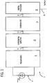
- FIG. 1 a simplified block diagram of an exemplary sensor, in this case shown to be a photosensor 2, is shown.
- the photosensor 2 includes a sensing device 4 that in this case is a photodiode coupled to an improved preamplifier or front end amplification section 6, which in turn outputs a signal 8 (or possibly more than one signal) to a differential amplifier 10.
- the differential amplifier 10 outputs an additional signal (or signals) 12 to a comparator 14, which in turn outputs a further signal (or signals) 16 to a digital processor 18.
- the digital processor 18 then is capable of providing an output signal 20 (or potentially more than one output signal) to another device or other devices, for example, an output device such as an LCD display, a computer, the internet or some other device or system that can utilize the information output by the digital processor 18.
- an output device such as an LCD display, a computer, the internet or some other device or system that can utilize the information output by the digital processor 18.
- the preamplifier 6 serves to take a signal or signals from the photodiode 4 and to amplify or at least pass a time-varying (e.g., AC) portion of those signals while filtering or rejecting a non-time-varying (e.g., DC) portion of those signals, such that the output signals 8 include only a time-varying component.
- the exact passband depends on the embodiment.
- the differential amplifier 10 it serves to amplify a difference between the signal 8 and another signal level, or potentially a difference between two signals provided as the signal 8.
- the comparator 14 typically in turn compares the output signal 12 from the differential amplifier with a particular comparison value or other standard, or even potentially compare two signals received from the differential amplifier 10 as the signal 12, and provide the signal 16 based upon that comparison.
- the digital processor 18 can perform a wide variety of operations based upon the signal or signals 16 received from the comparator 14 as well as other information received from other sources.
- the digital processor 18 in certain embodiments can be a microprocessor or other device capable of high levels of processing of the information received from the comparator, for the purpose of analysis or other purposes such as generating signals appropriate for driving output devices such as a display.
- the improved preamplifier 6 can take the form shown in FIGS. 4A and 4B in which all of the components of the preamplifier can be implemented on an integrated circuit, and even on the same integrated circuit on which are implemented the differential amplifier 10, the comparator 14 and the digital processor 18.
- photosensors employing the preamplifier 6 shown in FIGS. 4A and 4B can be physically smaller and less costly to manufacture than conventional photosensors employing preamplifiers such as those in FIGS. 2A-3B .
- the integrated circuit (or circuits) that are used to implement photosensors employing the preamplifier 6 shown in FIGS. 4A and 4B need not have as many leads/pins as integrated circuits implemented in conjunction with conventional preamplifiers such as those of FIGS. 2A-3B .
- the present invention is intended to encompass photosensors such as the photosensor 2 shown in FIG. 1 , it is also intended that the present invention encompass sensors of types other than photosensors, for example, vibration sensors, sound sensors, infrared sensors, other types of radiation sensors, position (or orientation/rotation) sensors, velocity or acceleration sensors, gravity sensors and other sensors. Further, the present invention is intended to encompass improved sensors utilizing improved preamplifiers such as that shown in FIGS. 4A-4B even when such sensors do not have each of a differential amplifier, comparator and digital processor (for example, in some cases, the sensors might only employ a differential amplifier and comparator in addition to the preamplifier, and the signals 16 from the comparator could be considered to be the output signals of the sensors).
- the present invention is intended to encompass not merely sensors having "preamplifier” circuits but rather is intended to encompass any preprocessing or processing circuitry, whether implemented in sensors or other applications, that serves to filter or otherwise process signals, and that can be fully implemented on an integrated circuit through the use of an integrated capacitor and bias-stabilizing current generating circuitry similar to that described below in relation to FIGS. 4A-4B .
- the preamplifier 22 includes a transimpedance amplifier (TIA) 24 including both an inverting amplifier 26 in parallel with a transimpedance feedback resistor 28 coupled between the input and output terminals of the operational amplifier 26.
- the TIA 24 is connected in series between the cathode of the photodiode 4 (the anode of which is connected to ground) and a capacitor 30.
- the capacitor 30 in turn is coupled in series between the TIA 24 and a high transconductance amplifier 32 having first and second input ports 34 and 36 and additionally first (inverting) and second (non-inverting) output ports 38 and 40, respectively.
- the two input ports 34 and 36 are coupled by way of a resistor 42. Additionally, while the first input port 34 is coupled to the capacitor 30, the second input port 36 is coupled to ground by way of a DC bias voltage source 44.
- the high transconductance amplifier 32 outputs across the output ports 38 and 40 a differential output current, which serves as the signal 8 shown in FIG. 1 and is provided to a differential amplifier such as the differential amplifier 10.
- FIG. 2B shows various circuit components that can be used to form the TIA 24 and the high transconductance amplifier 32 of FIG. 2A and which further can be implemented on an integrated circuit. Also evident from FIG. 2B are the output ports 38, 40 of the high transconductance amplifier 32, as well as the capacitor 30.
- the capacitor 30 in this embodiment necessarily is an discrete device external of the integrated circuit, due to its large size (in this case, 10 nanofarads). Because the external capacitor 30 is so large, and cannot be implemented on an integrated circuit, the integrated circuit on which the TIA 24 and the transconductance amplifier 32 are implemented must include first and second additional leads/pins 46 and 48, respectively, to which are coupled the leads of the capacitor 30.
- the preamplifier 22 shown in FIG. 2B is capable of satisfactorily operating as a preamplifier in a photosensor, the circuitry for the preamplifier cannot be reduced in size beyond a minimal amount of volume required to hold both the integrated circuit and the capacitor 30, and requires the special pins 46, 48 in order to mount the capacitor. For this reason, the preamplifier 22 is size-restricted, and manufacture of the preamplifier necessarily involves incurring costs relating to the implementation of the capacitor 30.
- FIG. 3A another conventional (Prior Art) embodiment of a preamplifier 52 that could be implemented in place of the preamplifier 6 of FIG. 1 is shown in a simplified schematic form, in combination with the photodiode 4.
- the preamplifier 52 includes a TIA 54 formed from the parallel combination of an inverting amplifier 56 and a transimpedance feedback resistor 58.
- the preamplifier 52 includes a high transconductance amplifier 62 having first and second input ports 64 and 66, respectively, which are coupled by way of a resistor 72, and also first (inverting) and second (non-inverting) output ports 68 and 70, respectively.
- the TIA 54 (in particular, the output node of the inverting amplifier 56 that is coupled to the transimpedance resistor 58) is the same node as the first input port 64 of the high transconductance amplifier 62, without any capacitor therebetween. Also, rather than coupling the second input port 66 of the transconductance amplifier 62 to a DC bias voltage source, the second port 66 instead is coupled to ground by way of a first capacitor 60.
- the input port of the TIA 54 to which the transimpedance feedback resistor 58 is coupled, is coupled both to ground by way of an additional resistor 74 and to the cathode of the photodiode 4 by way of a second capacitor 80, thus setting the appropriate bias voltage for the transconductance amplifier 62.
- the cathode of the photodiode 4 is also coupled to a positive DC voltage source 76 by way of a series combination of first and second additional resistors 78 and 82, respectively.
- a node between the resistors 78, 82 is also coupled to ground by way of an additional capacitor 84.
- the preamplifier 52 has not merely one external discrete device (e.g., the external capacitor 30 of FIG. 2B ) but rather has 5 external discrete devices including the capacitors 60, 80 and 84, as well as the resistors 78 and 82.
- the preamplifier 52 While having a larger number of external devices than the preamplifier 22, the preamplifier 52 requires only one additional pin/lead 86 allowing the capacitor 60 to be coupled to the high transconductance amplifier 62. In any event, as in the case of the preamplifier 22, the preamplifier 52 requires a number of external discrete devices that cannot be mounted on the integrated circuit and also requires at least one extra lead/pin be provided on the integrated circuit to accommodate these external devices.
- FIGS. 2A-3B show two conventional embodiments of preamplifiers
- another conventional design utilizes the output difference of dual photodiode and transimpedance amplifiers with different band pass regions, thus rejecting low frequency photo current.
- dual photodiode/transimpedance amplifier configurations require dual photodiodes, of which only one of the two photodiode/transimpedance amplifier circuits is sensitive to the desired time-varying signal.
- additional amplifiers e.g., a second transimpedance amplifier
- the preamplifier 102 includes a TIA 104 that includes an inverting amplifier 106 having input and output terminals that are coupled together by way of a transimpedance feedback resistor 108, with the input terminal also being coupled to the cathode of the photodiode 4.
- the preamplifier 102 includes a high transconductance amplifier 112 having first and second input ports 114 and 116, respectively, and first (inverting) and second (non-inverting) output ports 118 and 120, respectively.
- the output port of the TIA 104 is coupled to the first input port 114 of the high transconductance amplifier 120 by way of a capacitor 110.
- the capacitor 110 is much smaller than the capacitor 30 of the preamplifier 22 and, in the present embodiment, is 15 picofarads.
- the input ports 114 and 116 of the high transconductance amplifier 112 are respectively coupled to different respective ports of a low transconductance amplifier 122.
- the low transconductance amplifier 122 has an output port 124 that is coupled both to the first input port 114 of the high transconductance amplifier 112 and also to an inverting input 126 of the low transconductance amplifier 122.
- a DC biasing voltage source 128 is coupled between ground and each of the second input port 116 of the high transconductance amplifier 112 and also a non-inverting input 130 of the low transconductance amplifier 122.
- the preamplifier 102 operates as follows.
- the TIA 104 converts a current signal from the photodiode 4 into a voltage signal at the output of the TIA for receipt by the capacitor 110, with the voltage being related to the current by a factor of the resistance of the resistor 108 (e.g., by 60K).
- the capacitor 110 not only receives this voltage signal but also sees a low impedance circuit looking back towards the TIA 104 and the photodiode 4, such that the impedance looking back from the first input port 114 of the high transconductance amplifier 112 looking back towards the capacitor 110 appears to be merely the impedance/capacitance provided by that capacitor (e.g., 15 picofarads).
- the capacitor 110 while serving to link the TIA 104 with the transconductance amplifiers 112 and 122, also defines a frequency response with a low frequency cutoff such that low frequency signals and DC signals are not transmitted from the TIA to the transconductance amplifiers.
- high frequency (e.g., high frequency AC) signals that are of interest from the photodiode are transmitted to the transconductance amplifiers 112, 122, while any DC or low frequency (ambient) signals are filtered out/rejected.
- the low transconductance amplifier 122 serves to provide bias-stabilizing negative feedback current to the first input port 114 of the high transconductance amplifier 112.
- the bias-stabilizing feedback current which is a weak, AC ("push-pull") current, bias stabilizes the high transconductance amplifier 112.
- the low transconductance amplifier 122 tends to provide a current that charges the capacitor 110 so as to lift the voltage at the input port 114, and if the voltage at the input port 114 tends to increase above the voltage at the input port 116, then the low transconductance amplifier tends to output a current in relation to the capacitor 110 tending to reduce the voltage at the port 114.
- the low transconductance amplifier 122 tends to provide negative feedback such that the voltage at the input port 114 of the high transconductance amplifier 112 tracks the voltage of the port 116
- the AC signal communicated from the photodiode 4 by way of the TIA 104 and the capacitor 110 nevertheless tends to be reflected in the time-varying output at the output ports 118 and 120.
- the desired signal is passed within the pass band defined by the low frequency pull created by the capacitance value of the capacitor 110 and the bias-stabilizing feedback current and the high frequency pull of the amplifier roll-off.
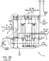
- the preamplifier 102 is shown in more detail along with the photodiode 4.
- the TIA 104 is formed by the combination of the resistor 108 coupled between base and collector terminals of a bipolar junction transistor (BJT) that forms the inverting amplifier 106, with the emitter of the BJT being coupled to ground.
- BJT bipolar junction transistor
- an additional small resistor 132 (which is optional, and which in the present embodiment prevents high-frequency peaking of the transimpedance amplifier output voltage due to the photodiode's capacitance) can also be coupled between the input port of the TIA 104 (and the resistor 108) and the photodiode 4.
- FIG. 4B also shows additional capacitances associated with the TIA 104 (e.g., a capacitance in parallel with the resistor 108 and capacitances between the output port of the TIA and ground), these are merely contended to represent stray capacitances and are not actual circuit elements.
- the high transconductance amplifier 112 in at least some embodiments includes first and second MOSFETs (metal oxide semiconductor field effect transistors) 134 and 136, which are N-type MOSFETs.
- the gate of the MOSFET 134 constitutes the first input port 114 of the high transconductance amplifier 112, and is coupled to the capacitor 110, which in turn is coupled to the resistor 108 and the BJT forming the inverting amplifier 106 of the TIA 104.
- the gate of the MOSFET 136 is the second input port 116 of the high transconductance amplifier 112 and is, as discussed in further detail below, coupled to several components of the low transconductance amplifier 122.
- the high transconductance amplifier 112 further includes, in addition to the MOSFETs 134 and 136, six additional BJTs 138, 140, 142, 144, 146 and 148, with the transistors 138, 142, 144 and 148 being NPN BJTs and the transistors 140 and 146 being PNP BJTs.
- the gate and drain of the MOSFET 134 is coupled to the emitter of the BJT 138, the collector of which is coupled to the base of the BJT 142.
- the base of the BJT 138 is coupled to the emitter of the BJT 140, the base of which is coupled to the emitter of the BJT 142.
- the drain and gate of the MOSFET 136 are coupled to the emitter of the BJT 148, the base of which is coupled to the emitter of the BJT 146 and the collector of which is coupled to the base of the BJT 144.
- the base of the BJT 146 further is coupled to the emitter of the BJT 144.
- the bases of the BJTs 140 and 146 are coupled together by way of a resistor 150 that conducts a differential current if there is a voltage differential between the voltages on the respective bases of the BJTs 140, 146. If such a differential current occurs through the resistor 150, then differential currents appear at the respective collectors of the BJTs 142 and 144, which respectively constitute the first and second output ports 118 and 120 of the high transconductance amplifier 112.
- the capacitor 110 is also coupled to the gate of an additional MOSFET 152 that constitutes the input port 126 of the low transconductance amplifier 122 and that, together with a MOSFET 154, form a differential pair of MOSFETs of the low transconductance amplifier 122.
- the gate of the MOSFET 154 is coupled to a node 156 between a resistor 158 and a series combination of a NPN BJT 160 and a PNP BJT 162.
- drains of the MOSFETs 152 and 154 are respectively coupled to respective sources of respective additional MOSFETs 164 and 166, which are P-type MOSFETS and together constitute a folded cascode of MOSFETs, the gates of MOSFETs 164 and 166 being coupled to the node 156. Because of the linking of the drains of the MOSFETs 152 and 154 with the sources of the MOSFETs 164 and 166, the currents within the drains of the MOSFETs 164 and 166 mirror those of the drains of the MOSFETs 152 and 154.
- a common drain of the MOSFET 164 and an additional series-connected MOSFET 168 is the output port 124 of the low transconductance amplifier 122 and is coupled both to the gate of the MOSFET 134 that is the first input port 114 of the high transconductance amplifier 112, as well as to the gate of the MOSFET 152 that is the inverting input port 126 of the low transconductance amplifier 122.
- the current communicated to or from the common drain of MOSFETs 164 and 168 is provided from or to the capacitor 110 that is coupled to each of the gates of the MOSFETs 134 and 152, and constitutes the negative bias-stabilizing feedback current of the low transconductance amplifier 122.
- MOSFETs 168, 170, 172, and 174 constitute a current mirror, reflecting the drain current of MOSFET 166 to the drain current of MOSFET 168.
- the preamplifier 102 additionally includes further MOSFETs and other components used to power and/or bias the other components discussed above. These include a set of two pairs of series coupled, mirrored MOSFETs 176 used to bias the output port of the TIA 104, where one of the series-connected pair of MOSFETs is coupled to that output port and the other of the pair of series-connected MOSFETs is coupled to ground by way of a pair of resistors 178.
- these include a set of five MOSFETs 180 including a first MOSFET 182 that is series coupled with a pair of mirrored MOSFETs 184 and 186 that are respectively coupled to the BJTs 138 and 140 and the BJTs 146 and 148, respectively. Additionally the set of MOSFETs 180 further includes two additional pairs of mirrored MOSFETs 188 and 190, where the MOSFETs 188 are respectively coupled to the MOSFET 134 and the collector of the BJT 138, and the MOSFETs 190 are respectively coupled to the MOSFET 136 and the collector of the BJT 148.
- the high transconductance amplifier 112 includes four further MOSFETs 192, 194, 196 and 198, with the MOSFETs 192 and 194 being respectively coupled to the MOSFETs 134 and 136, and the MOSFETs 196 and 198 being respectively coupled to the emitters of the BJTs 142 and 144, respectively, which are as discussed above also coupled to the respective opposite ends of the resistor 150.
- the low transconductance amplifier 122 also includes a series-connected pair of MOSFETs 200 that are coupled in series with the resistor 158 and BJTs 160 and 162, as well as a BJT 202 that is series-connected with a set of three mirrored MOSFETs 204, one of which is series-connected with an additional MOSFET 206 and the other two of which are respectively series coupled to the MOSFETs 164 and 166, respectively, as well as to the MOSFETs 152 and 154, respectively. Also as shown, each of the sources of the MOSFETs 152 and 154 is series-connected with a further MOSFET 218, which is coupled to ground.
- each of the MOSFETs 192, 194, 196, 198, 218 and 206 are all tied to a bias voltage (e.g., in the range of about 0.8 to 0.9 V) provided by a bias voltage source (not shown), such as a mirrored MOSFET.
- a bias voltage e.g., in the range of about 0.8 to 0.9 V
- the preamplifier 102 of FIGS. 4A and 4B is advantageous in comparison with each of the conventional preamplifiers described above with respect to FIGS. 2A-3B in several respects. Because the preamplifier 102 allows for the use of the capacitor 110, which is a small capacitor relative to the capacitor 30 of the preamplifier 22, the capacitor 110 can be implemented on the same integrated circuit on which all of the other components of the preamplifier are implemented, and potentially even all of the other components of the differential amplifier 10, the comparator 14 and the digital processor 18 of the photosensor 2 are implemented.
- the capacitor 110 can be an integrated capacitor that is integrated with the other components of the preamplifier and potentially the other components of the photosensor 2 (including even possibly, in some embodiments, the photodiode 4 itself), and no discrete components other than the photodiode 4 are required.
- the preamplifier 102 of FIGS. 4A and 4B can be implemented using an integrated circuit that has none of the extra leads/pins that were required in the embodiments of FIGS. 2A-3B to accommodate external components such as the capacitors 30, 60, 80 and 82, or the resistors 78 and 84.
- the integrated circuit can be implemented with only a minimum number of leads including two leads 208 and 210 by which the integrated circuit is coupled to the photodiode 4 (see FIG.
- the gain lead 216 is for controlling gain associated with another stage of circuitry implemented on the integrated circuit (e.g., the differential amplifier), albeit in alternate embodiments the gain lead or other control lead(s) could be utilized to control operation of a pre-amplifier circuit such as the circuit 102 shown.
- the leads corresponding to the output ports 118 and 120 need not be leads/pins external to the integrated circuit, but rather can be internal leads connecting the components of the preamplifier 102 to the components of the differential amplifier 10 that also can be implemented on the very same integrated circuit.
- the circuitry associated with the photosensor 2 can be reduced to as small of a size as is necessary to accommodate merely the integrated circuit and the minimum number of leads identified above, and indeed the photosensor can be implemented in an exceedingly simple manner involving merely the coupling of a photodiode to the leads 208 and 210 of the integrated circuit constituting the photosensor and then coupling the integrated circuit to power, ground and a control signal (or signals) as necessary and allowing for output signals as appropriate (e.g., by coupling the leads of the integrated circuit to leads on a circuit board).
- the preamplifier and the photosensor both can be manufactured with less difficulty and lower cost. Additionally, it is even possible in some other embodiments that the photodiode itself will be integrated as part of the integrated circuit, such that no external leads are required on the integrated circuit for coupling to the photodiode.
- manufacture of a sensor circuit merely requires mounting of the integrated circuit onto a circuit board (or other support structure), by which the integrated circuit can be coupled to a power source, ground, any control input(s) (e.g., a gain signal), and one or more device to which the integrated circuit is to provide output signals.
- a circuit board or other support structure
- the integrated circuit can be coupled to a power source, ground, any control input(s) (e.g., a gain signal), and one or more device to which the integrated circuit is to provide output signals.
- a further benefit provided by at least some embodiment of the present invention is improvement in signal to noise ratio by the additional rejection of low frequency noise internally generated by preceding amplification.
- Many sensors such as photosensors require a high sensitivity to modulated light from a light source, while rejecting ambient and low frequency light from sources such as natural and artificial lighting.
- the sensor can allow for detection of intensity differences that are greater than three orders of magnitude.
- an input device such as the photodiode 4, particularly an input device providing a low impedance/voltage output, could be coupled directly to the capacitor 110.
- transconductance amplifier 112 in the embodiment of FIGS. 4A-4B provides two differential current outputs, in alternate embodiments only a single output need be provided and/or the output or outputs could be voltage-type outputs.
Landscapes
- Engineering & Computer Science (AREA)
- Power Engineering (AREA)
- Amplifiers (AREA)
Claims (17)
- Schaltung zur Implementierung in einem Sensor, wobei die Schaltung umfasst:ein Mittel (104, 110) zum Filtern von mindestens einem aus einem Eingangssignal und einem weiteren Signal, das aus dem Eingangssignal abgeleitet wird, um ein Zwischensignal zu erzeugen;ein Mittel (112) zum Verstärken des Zwischensignals, um ein Ausgangssignal zu erzeugen, wobei das Mittel (112) zum Verstärken des Zwischensignals einen ersten Verstärker (112) mit einer zweiten Eingangsklemme (114) zum Empfangen des Zwischensignals, eine dritte Eingangsklemme (116) zum Empfangen einer Vorspannung, und eine zweite Ausgangsklemme (118, 120) aufweist;ein Mittel (122) zum Erzeugen eines Vorspannungsrückführsignals, wobei das Mittel (122) zum Erzeugen eines Vorspannungsrückführsignals einen zweiten Verstärker (122) mit einer vierten Eingangsklemme (126) umfasst, bei der es sich um eine invertierende Anschlussklemme zum Empfangen des Zwischensignals handelt, eine fünfte Eingangsklemme (130), bei der es sich um eine nicht invertierende Anschlussklemme zum Empfangen der Vorspannung handelt, und eine dritte Ausgangsklemme (124), wobei die dritte Ausgangsklemme (124) mit der zweiten Eingangsklemme (114) verbunden ist;wobei das Mittel (104, 110) zum Filtern des Weiteren einen Transimpedanzverstärker (104) und einen Kondensator (110) beinhaltet; wobeider Kondensator (110) eine erste Eingangsklemme aufweist, die mit einer einzelnen Ausgangsklemme des Transimpedanzverstärkers (104) verbunden ist, und eine erste Ausgangsklemme, die elektrisch mit der zweiten Eingangsklemme (114), der vierten Eingangsklemme (126) und der dritten Ausgangsklemme (124) verbunden ist, so dass der zweite Verstärker (122) einen Rückführstrom bezüglich des Kondensators (100) in Abhängigkeit von den Signalen bereitstellt, die an der vierten und fünften Eingangsklemme (126, 130) bereitgestellt werden;der Transimpedanzverstärker (104) eine sechste Eingangsklemme zum Empfangen des Eingangssignals von einer Sensorvorrichtung (4) umfasst; undder erste Verstärker (112) ein hoher Transkonduktanzverstärker ist und der zweite Verstärker (122) ein niedriger Transkonduktanzverstärker ist.
- Schaltung nach Anspruch 1, wobei:die Schaltung des Weiteren ein Mittel (10) zum weiteren Verstärken des Ausgangssignals beinhaltet; oderdie Schaltung des Weiteren ein Mittel zum Verarbeiten von mindestens einem aus dem Ausgangssignal und einem Ableitungssignal beinhaltet, das zumindest indirekt auf dem Ausgangssignal basiert, wobei das Mittel zum Verarbeiten mindestens eines aus einem Komparator und einem digitalen Prozessor beinhaltet; oderwobei die Schaltung des Weiteren die Sensorvorrichtung (4) beinhaltet, die das Eingangssignal bereitstellt.
- Schaltung nach Anspruch 1, wobei:der Kondensator (110) eine ausreichend geringe Größe aufweist, um mit jedem der Verstärker auf einer integrierten Schaltung implementiert zu werden; oderder Rückführstrom ein negativer Vorspannungsrückführstrom ist; oderder Kondensator (110) als ein Hochpassfilter dient; oderdie Schaltung eine Vorverstärkungsschaltung ist;
- Schaltung nach Anspruch 1, wobei
der Kondensator (110) eine ausreichend geringe Größe aufweist, um mit jedem der Verstärker auf einer integrierten Schaltung implementiert zu werden; und
die erste Eingangsklemme des Kondensators (110) ein Spannungseingangssignal von einer Schaltung mit einem niederohmigen Ausgang empfängt. - Schaltung nach Anspruch 1, wobei:
der erste Verstärker (112) dazu konfiguriert ist, ein Paar von verschiedenen Stromausgangssignalen bereitzustellen. - Schaltung nach Anspruch 1, wobei
die Sensorvorrichtung (4) eine Fotodiode ist; oder
jeder der Verstärker (112, 122) und der Kondensator (110) auf mindestens einer integrierten Schaltung implementiert sind; oder
jedes aus der Sensorvorrichtung (4), dem Kondensator (110) und den zwei Verstärkern (112, 122) auf einer einzelnen integrierten Schaltung implementiert ist. - Schaltung nach Anspruch 1, wobei mindestens einer aus dem ersten (112) und dem zweiten (122) Verstärker aus einer Vielzahl von Metalloxid-Halbleiter-Feldeffekttransistoren besteht, und wobei mindestens zwei aus der zweiten (114), der dritten (116), der vierten (126) und der fünften (130) Eingangsklemme als jeweilige Gates des ersten und zweiten Metalloxid-Halbleiter-Feldeffekttransistors ausgebildet sind.
- Integrierte Schaltung, auf der die Schaltung nach einem der Ansprüche 1 bis 7 implementiert ist, wobei die integrierte Schaltung beinhaltet:eine Vielzahl von externen Leitungen, wobei die Vielzahl von externen Leitungen auf nicht mehr als eine Versorgungsleitung, eine Masseleitung, eine Verstärkungsleitung, mindestens eine Sensorvorrichtungsleitung und mindestens eine Ausgangssignalleitung beschränkt ist; undeinen Differenzialverstärker (10),einen Komparator (14), odereinen digitalen Prozessor (18).
- Integrierte Schaltung nach Anspruch 8, wobei die integrierte Schaltung den Differenzialverstärker (10), den Komparator (14) und den digitalen Prozessor (18) beinhaltet; wobei
die integrierte Schaltung des Weiteren die Sensorvorrichtung (4) umfasst, die elektrisch mit der ersten Eingangsklemme des Kondensators (110) verbunden ist, den Differenzialverstärker (10), der elektrisch mit der zweiten Ausgangsklemme des ersten Verstärkers (112) verbunden ist, den Komparator (14), der mit dem Differenzialverstärker (10) verbunden ist, und den digitalen Prozessor (18), der mit dem Komparator (14) verbunden ist; und
wobei die integrierte Schaltung mindestens eine Leitung beinhaltet, durch die mindestens ein Ausgangssignal von dem digitalen Prozessor an eine externe Vorrichtung bereitgestellt wird, wobei die externe Vorrichtung mindestens eines aus einem Mikroprozessor, einem Computer, einem Netzwerk und einem drahtlosen Sender beinhaltet. - Fotosensor, umfassend die Schaltung nach einem der Ansprüche 1 bis 9 und eine Fotodiode.
- Fotosensor nach Anspruch 10, wobei die Fotodiode mit der Schaltung verbunden ist und eine Stromanzeige dafür bereitstellt.
- Sensor, umfassend die Schaltung nach einem der Ansprüche 1 bis 9, wobei der Sensor ein Strahlungssensor, ein Licht, ein Positionssensor, ein Geschwindigkeitssensor, ein Beschleunigungssensor, ein Schwerkraftsensor, ein Schwingungssensor oder ein Klangsensor ist.
- Verfahren zum Betreiben eines Sensors, wobei das Verfahren umfasst:i) Bereitstellen eines Eingangssignals von einer Sensorvorrichtung;ii) Verstärken des Zwischensignals, das zumindest zum Teil aus dem Eingangssignal mithilfe eines Transimpedanzverstärkers (104) abgeleitet wird, mithilfe eines ersten Verstärkers (112), um ein Ausgangssignal zu erzeugen, wobei der erste Verstärker (112) eine zweite (114) und dritte (116) Eingangsklemme und eine zweite Ausgangsklemme (118, 120) aufweist; undiii) Erzeugen eines Vorspannungsrückführsignals mithilfe eines zweiten Verstärkers (122), um die Verstärkung zu beeinflussen, wobei der zweite Verstärker (122) eine vierte Eingangsklemme (126) aufweist, bei der es sich um eine invertierende Anschlussklemme handelt, und eine fünfte Eingangsklemme (130), bei der es sich um eine nicht invertierende Anschlussklemme handelt, und eine dritte Ausgangsklemme (124);
wobei das Zwischensignal mithilfe eines Kondensators (110) abgeleitet wird, dessen erste Eingangsklemme mit einer einzelnen Ausgangsklemme des Transimpedanzverstärkers (104) verbunden ist, und dessen erste Ausgangsklemme elektrisch mit der zweiten Eingangsklemme (114), der vierten Eingangsklemme (126) und der dritten Ausgangsklemme (124) verbunden ist;
wobei das Vorspannungsrückführsignal bezüglich des Kondensators (110) in Abhängigkeit von Signalen erzeugt wird, die für die vierte Eingangsklemme (126) und die fünfte Eingangsklemme (130) bereitgestellt werden; und
mindestens die Schritte ii) bis iii) durch eine integrierte Schaltung ausgeführt werden; undiv) Anlegen einer Vorspannung aus einer Vorspannungsquelle an die dritte Anschlussklemme (116); undv) Einstellen der fünften Eingangsklemme (130) auf die Vorspannung;
wobei
der erste Verstärker (112) ein hoher Transkonduktanzverstärker ist und der zweite Verstärker (122) ein niedriger Transkonduktanzverstärker ist. - Verfahren nach Anspruch 13, des Weiteren umfassend das Filtern von mindestens einem aus dem Eingangssignal und einem weiteren Signal, das aus dem Eingangssignal mithilfe des Kondensators (110) abgeleitet wird, um das Zwischensignal zu erzeugen.
- Verfahren nach Anspruch 13, des Weiteren umfassend das Verstärken des Eingangssignals, um das weitere Signal zu erzeugen, das dann gefiltert wird.
- Verfahren nach Anspruch 13, wobei:das Eingangssignal zumindest indirekt von der Sensorvorrichtung empfangen wird, die auch auf der integrierten Schaltung implementiert ist; oderder Sensor ein Fotosensor ist und das Eingangssignal zumindest indirekt von einer Fotodiode empfangen wird.
- Verfahren nach Anspruch 14, wobei das Filtern durch den Transimpedanzverstärker (104) ausgeführt wird.
Applications Claiming Priority (1)
| Application Number | Priority Date | Filing Date | Title |
|---|---|---|---|
| US11/333,717 US7358819B2 (en) | 2006-01-17 | 2006-01-17 | Reduced-size sensor circuit |
Publications (3)
| Publication Number | Publication Date |
|---|---|
| EP1808960A2 EP1808960A2 (de) | 2007-07-18 |
| EP1808960A3 EP1808960A3 (de) | 2007-08-22 |
| EP1808960B1 true EP1808960B1 (de) | 2018-09-19 |
Family
ID=37944719
Family Applications (1)
| Application Number | Title | Priority Date | Filing Date |
|---|---|---|---|
| EP07000919.6A Ceased EP1808960B1 (de) | 2006-01-17 | 2007-01-17 | Verkleinerte Sensorschaltung |
Country Status (2)
| Country | Link |
|---|---|
| US (1) | US7358819B2 (de) |
| EP (1) | EP1808960B1 (de) |
Families Citing this family (20)
| Publication number | Priority date | Publication date | Assignee | Title |
|---|---|---|---|---|
| USRE46672E1 (en) | 2006-07-13 | 2018-01-16 | Velodyne Lidar, Inc. | High definition LiDAR system |
| JP5185354B2 (ja) * | 2010-11-26 | 2013-04-17 | リズム時計工業株式会社 | 光学モーションセンサー |
| US9762234B2 (en) * | 2011-02-10 | 2017-09-12 | Synaptics Incorporated | Input device interference determination |
| DE102012207276B4 (de) | 2011-08-01 | 2018-04-05 | Continental Automotive Gmbh | Vollaktiver Piezostack mit Passivierung |
| US9184957B2 (en) | 2012-12-27 | 2015-11-10 | Intel Corporation | High speed receivers circuits and methods |
| US9048777B2 (en) * | 2012-12-31 | 2015-06-02 | Silicon Laboratories Inc. | Apparatus for integrated circuit interface and associated methods |
| US10175271B2 (en) * | 2012-12-31 | 2019-01-08 | Silicon Laboratories Inc. | Apparatus for differencing comparator and associated methods |
| US10627490B2 (en) | 2016-01-31 | 2020-04-21 | Velodyne Lidar, Inc. | Multiple pulse, LIDAR based 3-D imaging |
| CA3017735C (en) | 2016-03-19 | 2023-03-14 | Velodyne Lidar, Inc. | Integrated illumination and detection for lidar based 3-d imaging |
| WO2017210418A1 (en) | 2016-06-01 | 2017-12-07 | Velodyne Lidar, Inc. | Multiple pixel scanning lidar |
| JP7290571B2 (ja) | 2017-03-31 | 2023-06-13 | ベロダイン ライダー ユーエスエー,インコーポレイテッド | 統合化されたlidar照明出力制御 |
| JP2020519881A (ja) | 2017-05-08 | 2020-07-02 | ベロダイン ライダー, インク. | Lidarデータ収集及び制御 |
| US11294041B2 (en) * | 2017-12-08 | 2022-04-05 | Velodyne Lidar Usa, Inc. | Systems and methods for improving detection of a return signal in a light ranging and detection system |
| US11029406B2 (en) * | 2018-04-06 | 2021-06-08 | Luminar, Llc | Lidar system with AlInAsSb avalanche photodiode |
| US11971507B2 (en) | 2018-08-24 | 2024-04-30 | Velodyne Lidar Usa, Inc. | Systems and methods for mitigating optical crosstalk in a light ranging and detection system |
| US10712434B2 (en) | 2018-09-18 | 2020-07-14 | Velodyne Lidar, Inc. | Multi-channel LIDAR illumination driver |
| US11082010B2 (en) | 2018-11-06 | 2021-08-03 | Velodyne Lidar Usa, Inc. | Systems and methods for TIA base current detection and compensation |
| US12061263B2 (en) | 2019-01-07 | 2024-08-13 | Velodyne Lidar Usa, Inc. | Systems and methods for a configurable sensor system |
| US11885958B2 (en) | 2019-01-07 | 2024-01-30 | Velodyne Lidar Usa, Inc. | Systems and methods for a dual axis resonant scanning mirror |
| US10613203B1 (en) | 2019-07-01 | 2020-04-07 | Velodyne Lidar, Inc. | Interference mitigation for light detection and ranging |
Citations (4)
| Publication number | Priority date | Publication date | Assignee | Title |
|---|---|---|---|---|
| US6292052B1 (en) * | 2000-03-06 | 2001-09-18 | Tektronix, Inc. | Output amplifier for a discrete filter-less optical reference receiver |
| US20020101270A1 (en) * | 2001-01-30 | 2002-08-01 | Fujitsu Limited | Current pulse receiving circuit |
| US6762596B2 (en) * | 2001-09-12 | 2004-07-13 | Sharp Kabushiki Kaisha | Constant voltage circuit and infrared remote control receiver using the same |
| US20060002720A1 (en) * | 2004-05-14 | 2006-01-05 | Naoki Nishiyama | Optical receiving unit reducing cross talk between optical transmitting unit and optical transmitting/receiving apparatus installing the same |
Family Cites Families (8)
| Publication number | Priority date | Publication date | Assignee | Title |
|---|---|---|---|---|
| US3989959A (en) * | 1975-08-28 | 1976-11-02 | Vitatron Medical B.V. | Low current drain amplifier incorporating feedback means for establishing sensitivity |
| US5182477A (en) * | 1990-03-22 | 1993-01-26 | Silicon Systems, Inc. | Bipolar tunable transconductance element |
| US5808296A (en) * | 1996-03-22 | 1998-09-15 | Banner Engineering Corporation | Programmable detection sensor with means to automatically adjust sensor operating characteristics to optimize performance for both high gain and low contrast applications |
| US6784750B2 (en) * | 2002-04-09 | 2004-08-31 | Microsemi Corporation | Transimpedance amplifier with selective DC compensation |
| US6803825B2 (en) * | 2002-04-09 | 2004-10-12 | Microsemi Corporation | Pseudo-differential transimpedance amplifier |
| US6822515B2 (en) * | 2002-07-19 | 2004-11-23 | Ikuroh Ichitsubo | Accurate power sensing circuit for power amplifiers |
| US7184799B1 (en) * | 2003-05-14 | 2007-02-27 | Marvell International Ltd. | Method and apparatus for reducing wake up time of a powered down device |
| US7199652B2 (en) * | 2003-11-21 | 2007-04-03 | Matsushita Electric Industrial Co., Ltd. | Amplifier; and transmitter and communication device incorporating the same |
-
2006
- 2006-01-17 US US11/333,717 patent/US7358819B2/en not_active Expired - Lifetime
-
2007
- 2007-01-17 EP EP07000919.6A patent/EP1808960B1/de not_active Ceased
Patent Citations (4)
| Publication number | Priority date | Publication date | Assignee | Title |
|---|---|---|---|---|
| US6292052B1 (en) * | 2000-03-06 | 2001-09-18 | Tektronix, Inc. | Output amplifier for a discrete filter-less optical reference receiver |
| US20020101270A1 (en) * | 2001-01-30 | 2002-08-01 | Fujitsu Limited | Current pulse receiving circuit |
| US6762596B2 (en) * | 2001-09-12 | 2004-07-13 | Sharp Kabushiki Kaisha | Constant voltage circuit and infrared remote control receiver using the same |
| US20060002720A1 (en) * | 2004-05-14 | 2006-01-05 | Naoki Nishiyama | Optical receiving unit reducing cross talk between optical transmitting unit and optical transmitting/receiving apparatus installing the same |
Also Published As
| Publication number | Publication date |
|---|---|
| US7358819B2 (en) | 2008-04-15 |
| US20070164825A1 (en) | 2007-07-19 |
| EP1808960A3 (de) | 2007-08-22 |
| EP1808960A2 (de) | 2007-07-18 |
Similar Documents
| Publication | Publication Date | Title |
|---|---|---|
| EP1808960A2 (de) | Verkleinerte Sensorschaltung | |
| JP3541750B2 (ja) | 光受信前置増幅器 | |
| US7276965B1 (en) | Nested transimpedance amplifier | |
| JPH1183624A (ja) | 赤外線検出装置 | |
| JP2017152776A (ja) | 光受信回路 | |
| CN106788280B (zh) | 一种低噪高速跨阻放大器 | |
| US6054901A (en) | Low noise preamplifier | |
| CN101488808A (zh) | 一种跨阻补偿式光接收机 | |
| CN113654460A (zh) | 一种适用于光镊系统位置探测的差分四象限光电探测器 | |
| EP0127743A2 (de) | Lichtdetektionsschaltung | |
| JP4011317B2 (ja) | 定電圧回路およびそれを用いる赤外線リモコン受信機 | |
| CN102437823B (zh) | 宽带低噪声传感器放大电路 | |
| WO2005101538A2 (en) | Transconductance circuit for piezoelectric transducer | |
| US7659780B2 (en) | Gain control circuit | |
| CN110546883A (zh) | 跨阻放大器电路 | |
| US6768384B1 (en) | High-speed differential preamplifier | |
| JP3217806B2 (ja) | 光検出回路 | |
| KR100509907B1 (ko) | 포토 다이오드 회로 | |
| CN113316895B (zh) | 一种放大电路 | |
| CN209627330U (zh) | 提升跨阻放大电路中rssi脚抗噪能力的电路 | |
| JP3844544B2 (ja) | 光受信回路 | |
| JP4567177B2 (ja) | 広帯域プリアンプ | |
| US7518447B1 (en) | Transimpedance amplifier | |
| JPH10318834A (ja) | 焦電型赤外線検出装置 | |
| CN108900187B (zh) | 一种光电二极管差分信号的获取电路 |
Legal Events
| Date | Code | Title | Description |
|---|---|---|---|
| PUAI | Public reference made under article 153(3) epc to a published international application that has entered the european phase |
Free format text: ORIGINAL CODE: 0009012 |
|
| AK | Designated contracting states |
Kind code of ref document: A2 Designated state(s): AT BE BG CH CY CZ DE DK EE ES FI FR GB GR HU IE IS IT LI LT LU LV MC NL PL PT RO SE SI SK TR |
|
| AX | Request for extension of the european patent |
Extension state: AL BA HR MK YU |
|
| PUAL | Search report despatched |
Free format text: ORIGINAL CODE: 0009013 |
|
| AK | Designated contracting states |
Kind code of ref document: A3 Designated state(s): AT BE BG CH CY CZ DE DK EE ES FI FR GB GR HU IE IS IT LI LT LU LV MC NL PL PT RO SE SI SK TR |
|
| AX | Request for extension of the european patent |
Extension state: AL BA HR MK YU |
|
| 17P | Request for examination filed |
Effective date: 20080222 |
|
| 17Q | First examination report despatched |
Effective date: 20080328 |
|
| AKX | Designation fees paid |
Designated state(s): DE FR GB IT |
|
| STAA | Information on the status of an ep patent application or granted ep patent |
Free format text: STATUS: EXAMINATION IS IN PROGRESS |
|
| GRAP | Despatch of communication of intention to grant a patent |
Free format text: ORIGINAL CODE: EPIDOSNIGR1 |
|
| STAA | Information on the status of an ep patent application or granted ep patent |
Free format text: STATUS: GRANT OF PATENT IS INTENDED |
|
| GRAJ | Information related to disapproval of communication of intention to grant by the applicant or resumption of examination proceedings by the epo deleted |
Free format text: ORIGINAL CODE: EPIDOSDIGR1 |
|
| GRAP | Despatch of communication of intention to grant a patent |
Free format text: ORIGINAL CODE: EPIDOSNIGR1 |
|
| INTG | Intention to grant announced |
Effective date: 20180130 |
|
| GRAJ | Information related to disapproval of communication of intention to grant by the applicant or resumption of examination proceedings by the epo deleted |
Free format text: ORIGINAL CODE: EPIDOSDIGR1 |
|
| STAA | Information on the status of an ep patent application or granted ep patent |
Free format text: STATUS: EXAMINATION IS IN PROGRESS |
|
| INTG | Intention to grant announced |
Effective date: 20180223 |
|
| INTG | Intention to grant announced |
Effective date: 20180223 |
|
| INTC | Intention to grant announced (deleted) | ||
| GRAP | Despatch of communication of intention to grant a patent |
Free format text: ORIGINAL CODE: EPIDOSNIGR1 |
|
| STAA | Information on the status of an ep patent application or granted ep patent |
Free format text: STATUS: GRANT OF PATENT IS INTENDED |
|
| INTG | Intention to grant announced |
Effective date: 20180430 |
|
| GRAS | Grant fee paid |
Free format text: ORIGINAL CODE: EPIDOSNIGR3 |
|
| GRAA | (expected) grant |
Free format text: ORIGINAL CODE: 0009210 |
|
| STAA | Information on the status of an ep patent application or granted ep patent |
Free format text: STATUS: THE PATENT HAS BEEN GRANTED |
|
| AK | Designated contracting states |
Kind code of ref document: B1 Designated state(s): DE FR GB IT |
|
| REG | Reference to a national code |
Ref country code: GB Ref legal event code: FG4D |
|
| REG | Reference to a national code |
Ref country code: DE Ref legal event code: R096 Ref document number: 602007056162 Country of ref document: DE |
|
| PG25 | Lapsed in a contracting state [announced via postgrant information from national office to epo] |
Ref country code: IT Free format text: LAPSE BECAUSE OF FAILURE TO SUBMIT A TRANSLATION OF THE DESCRIPTION OR TO PAY THE FEE WITHIN THE PRESCRIBED TIME-LIMIT Effective date: 20180919 |
|
| REG | Reference to a national code |
Ref country code: DE Ref legal event code: R097 Ref document number: 602007056162 Country of ref document: DE |
|
| PLBE | No opposition filed within time limit |
Free format text: ORIGINAL CODE: 0009261 |
|
| STAA | Information on the status of an ep patent application or granted ep patent |
Free format text: STATUS: NO OPPOSITION FILED WITHIN TIME LIMIT |
|
| 26N | No opposition filed |
Effective date: 20190620 |
|
| PGFP | Annual fee paid to national office [announced via postgrant information from national office to epo] |
Ref country code: FR Payment date: 20191219 Year of fee payment: 14 |
|
| PGFP | Annual fee paid to national office [announced via postgrant information from national office to epo] |
Ref country code: DE Payment date: 20191218 Year of fee payment: 14 Ref country code: GB Payment date: 20191224 Year of fee payment: 14 |
|
| REG | Reference to a national code |
Ref country code: DE Ref legal event code: R119 Ref document number: 602007056162 Country of ref document: DE |
|
| GBPC | Gb: european patent ceased through non-payment of renewal fee |
Effective date: 20210117 |
|
| PG25 | Lapsed in a contracting state [announced via postgrant information from national office to epo] |
Ref country code: FR Free format text: LAPSE BECAUSE OF NON-PAYMENT OF DUE FEES Effective date: 20210131 |
|
| PG25 | Lapsed in a contracting state [announced via postgrant information from national office to epo] |
Ref country code: GB Free format text: LAPSE BECAUSE OF NON-PAYMENT OF DUE FEES Effective date: 20210117 Ref country code: DE Free format text: LAPSE BECAUSE OF NON-PAYMENT OF DUE FEES Effective date: 20210803 |