EP1811547A1 - Optischer integrierer, optische beleuchtungsvorrichtung, belichtungsvorrichtung und belichtungsverfahren - Google Patents
Optischer integrierer, optische beleuchtungsvorrichtung, belichtungsvorrichtung und belichtungsverfahren Download PDFInfo
- Publication number
- EP1811547A1 EP1811547A1 EP06712307A EP06712307A EP1811547A1 EP 1811547 A1 EP1811547 A1 EP 1811547A1 EP 06712307 A EP06712307 A EP 06712307A EP 06712307 A EP06712307 A EP 06712307A EP 1811547 A1 EP1811547 A1 EP 1811547A1
- Authority
- EP
- European Patent Office
- Prior art keywords
- mirror
- optical
- elements
- exposure
- mask
- Prior art date
- Legal status (The legal status is an assumption and is not a legal conclusion. Google has not performed a legal analysis and makes no representation as to the accuracy of the status listed.)
- Withdrawn
Links
Images






Classifications
-
- G—PHYSICS
- G03—PHOTOGRAPHY; CINEMATOGRAPHY; ANALOGOUS TECHNIQUES USING WAVES OTHER THAN OPTICAL WAVES; ELECTROGRAPHY; HOLOGRAPHY
- G03F—PHOTOMECHANICAL PRODUCTION OF TEXTURED OR PATTERNED SURFACES, e.g. FOR PRINTING, FOR PROCESSING OF SEMICONDUCTOR DEVICES; MATERIALS THEREFOR; ORIGINALS THEREFOR; APPARATUS SPECIALLY ADAPTED THEREFOR
- G03F7/00—Photomechanical, e.g. photolithographic, production of textured or patterned surfaces, e.g. printing surfaces; Materials therefor, e.g. comprising photoresists; Apparatus specially adapted therefor
- G03F7/70—Microphotolithographic exposure; Apparatus therefor
- G03F7/70058—Mask illumination systems
- G03F7/70075—Homogenization of illumination intensity in the mask plane by using an integrator, e.g. fly's eye lens, facet mirror or glass rod, by using a diffusing optical element or by beam deflection
-
- G—PHYSICS
- G02—OPTICS
- G02B—OPTICAL ELEMENTS, SYSTEMS OR APPARATUS
- G02B17/00—Systems with reflecting surfaces, with or without refracting elements
- G02B17/002—Arrays of reflective systems
-
- G—PHYSICS
- G02—OPTICS
- G02B—OPTICAL ELEMENTS, SYSTEMS OR APPARATUS
- G02B17/00—Systems with reflecting surfaces, with or without refracting elements
- G02B17/02—Catoptric systems, e.g. image erecting and reversing system
- G02B17/06—Catoptric systems, e.g. image erecting and reversing system using mirrors only, i.e. having only one curved mirror
- G02B17/0647—Catoptric systems, e.g. image erecting and reversing system using mirrors only, i.e. having only one curved mirror using more than three curved mirrors
- G02B17/0657—Catoptric systems, e.g. image erecting and reversing system using mirrors only, i.e. having only one curved mirror using more than three curved mirrors off-axis or unobscured systems in which all of the mirrors share a common axis of rotational symmetry
-
- G—PHYSICS
- G02—OPTICS
- G02B—OPTICAL ELEMENTS, SYSTEMS OR APPARATUS
- G02B17/00—Systems with reflecting surfaces, with or without refracting elements
- G02B17/02—Catoptric systems, e.g. image erecting and reversing system
- G02B17/06—Catoptric systems, e.g. image erecting and reversing system using mirrors only, i.e. having only one curved mirror
- G02B17/0647—Catoptric systems, e.g. image erecting and reversing system using mirrors only, i.e. having only one curved mirror using more than three curved mirrors
- G02B17/0663—Catoptric systems, e.g. image erecting and reversing system using mirrors only, i.e. having only one curved mirror using more than three curved mirrors off-axis or unobscured systems in which not all of the mirrors share a common axis of rotational symmetry, e.g. at least one of the mirrors is warped, tilted or decentered with respect to the other elements
-
- G—PHYSICS
- G02—OPTICS
- G02B—OPTICAL ELEMENTS, SYSTEMS OR APPARATUS
- G02B19/00—Condensers, e.g. light collectors or similar non-imaging optics
- G02B19/0004—Condensers, e.g. light collectors or similar non-imaging optics characterised by the optical means employed
- G02B19/0019—Condensers, e.g. light collectors or similar non-imaging optics characterised by the optical means employed having reflective surfaces only (e.g. louvre systems, systems with multiple planar reflectors)
- G02B19/0023—Condensers, e.g. light collectors or similar non-imaging optics characterised by the optical means employed having reflective surfaces only (e.g. louvre systems, systems with multiple planar reflectors) at least one surface having optical power
-
- G—PHYSICS
- G02—OPTICS
- G02B—OPTICAL ELEMENTS, SYSTEMS OR APPARATUS
- G02B19/00—Condensers, e.g. light collectors or similar non-imaging optics
- G02B19/0004—Condensers, e.g. light collectors or similar non-imaging optics characterised by the optical means employed
- G02B19/0028—Condensers, e.g. light collectors or similar non-imaging optics characterised by the optical means employed refractive and reflective surfaces, e.g. non-imaging catadioptric systems
-
- G—PHYSICS
- G02—OPTICS
- G02B—OPTICAL ELEMENTS, SYSTEMS OR APPARATUS
- G02B19/00—Condensers, e.g. light collectors or similar non-imaging optics
- G02B19/0033—Condensers, e.g. light collectors or similar non-imaging optics characterised by the use
- G02B19/0047—Condensers, e.g. light collectors or similar non-imaging optics characterised by the use for use with a light source
-
- G—PHYSICS
- G02—OPTICS
- G02B—OPTICAL ELEMENTS, SYSTEMS OR APPARATUS
- G02B19/00—Condensers, e.g. light collectors or similar non-imaging optics
- G02B19/0033—Condensers, e.g. light collectors or similar non-imaging optics characterised by the use
- G02B19/0095—Condensers, e.g. light collectors or similar non-imaging optics characterised by the use for use with ultraviolet radiation
-
- G—PHYSICS
- G02—OPTICS
- G02B—OPTICAL ELEMENTS, SYSTEMS OR APPARATUS
- G02B27/00—Optical systems or apparatus not provided for by any of the groups G02B1/00 - G02B26/00, G02B30/00
- G02B27/09—Beam shaping, e.g. changing the cross-sectional area, not otherwise provided for
- G02B27/0905—Dividing and/or superposing multiple light beams
-
- G—PHYSICS
- G02—OPTICS
- G02B—OPTICAL ELEMENTS, SYSTEMS OR APPARATUS
- G02B27/00—Optical systems or apparatus not provided for by any of the groups G02B1/00 - G02B26/00, G02B30/00
- G02B27/09—Beam shaping, e.g. changing the cross-sectional area, not otherwise provided for
- G02B27/0938—Using specific optical elements
- G02B27/0977—Reflective elements
- G02B27/0983—Reflective elements being curved
-
- G—PHYSICS
- G03—PHOTOGRAPHY; CINEMATOGRAPHY; ANALOGOUS TECHNIQUES USING WAVES OTHER THAN OPTICAL WAVES; ELECTROGRAPHY; HOLOGRAPHY
- G03F—PHOTOMECHANICAL PRODUCTION OF TEXTURED OR PATTERNED SURFACES, e.g. FOR PRINTING, FOR PROCESSING OF SEMICONDUCTOR DEVICES; MATERIALS THEREFOR; ORIGINALS THEREFOR; APPARATUS SPECIALLY ADAPTED THEREFOR
- G03F7/00—Photomechanical, e.g. photolithographic, production of textured or patterned surfaces, e.g. printing surfaces; Materials therefor, e.g. comprising photoresists; Apparatus specially adapted therefor
- G03F7/70—Microphotolithographic exposure; Apparatus therefor
- G03F7/70058—Mask illumination systems
- G03F7/702—Reflective illumination, i.e. reflective optical elements other than folding mirrors, e.g. extreme ultraviolet [EUV] illumination systems
-
- G—PHYSICS
- G02—OPTICS
- G02B—OPTICAL ELEMENTS, SYSTEMS OR APPARATUS
- G02B27/00—Optical systems or apparatus not provided for by any of the groups G02B1/00 - G02B26/00, G02B30/00
- G02B27/09—Beam shaping, e.g. changing the cross-sectional area, not otherwise provided for
- G02B27/0938—Using specific optical elements
- G02B27/095—Refractive optical elements
- G02B27/0955—Lenses
- G02B27/0961—Lens arrays
-
- G—PHYSICS
- G02—OPTICS
- G02B—OPTICAL ELEMENTS, SYSTEMS OR APPARATUS
- G02B7/00—Mountings, adjusting means, or light-tight connections, for optical elements
- G02B7/02—Mountings, adjusting means, or light-tight connections, for optical elements for lenses
- G02B7/14—Mountings, adjusting means, or light-tight connections, for optical elements for lenses adapted to interchange lenses
- G02B7/16—Rotatable turrets
Definitions
- the present invention relates to an optical integrator, illumination optical apparatus, exposure apparatus, and exposure method. More particularly, the present invention relates to an illumination optical apparatus in an exposure apparatus used for fabricating micro devices such as semiconductor devices, image pickup devices, liquid-crystal display devices, and thin-film magnetic heads by lithography.
- the conventional exposure apparatus used in fabrication of semiconductor devices and others is arranged to project a circuit pattern formed on a mask (reticle), through a projection optical system onto a photosensitive substrate (e.g., a wafer) to transfer the circuit pattern onto the photosensitive substrate.
- the photosensitive substrate is coated with a resist, and the projection exposure through the projection optical system results in exposing the resist to light and obtaining a resist pattern corresponding to the mask pattern.
- the resolving power W of exposure apparatus is dependent upon the wavelength ⁇ of exposure light and the numerical aperture NA of the projection optical system and is expressed by Eq (a) below.
- W k ⁇ ⁇ / NA k : constant
- EUVL ExtraViolet Lithography
- the EUVL exposure apparatus uses EUV (Extreme UltraViolet) light in the wavelength range of approximately 5-20 nm, in comparison with the conventional exposure methods using KrF excimer laser light at the wavelength of 248 nm and ArF excimer laser light at the wavelength of 193 nm.
- EUV Extreme UltraViolet
- the EUVL exposure apparatus necessarily uses a reflective optical integrator, a reflective mask, and a reflective projection optical system (e.g., cf. Patent Document 1).
- Patent Document 1 Japanese Patent Application Laid-Open No. 11-312638
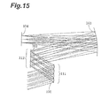
- the conventional reflective optical integrator disclosed in Patent Document 1 is comprised, as shown in Fig. 15, of a first reflecting element group 111 consisting of a plurality of concave reflector elements 101 arranged in parallel, and a second reflecting element group 112 consisting of a plurality of concave reflector elements 102 arranged in parallel.
- Parallel light incident to the entrance-side first reflecting element group 111 is divided by the individual concave reflector elements 101 to be focused on or near the corresponding concave reflector elements 102 of the exit-side second reflecting element group 112.
- Rays diverging from a point on one concave reflector element 101 in the first reflecting element group 111 are focused via a corresponding concave reflector element 102 in the second reflecting element group 112 and via a condenser optical system 103 on a surface to be illuminated (a pattern surface of reflective mask) 104.
- the entrance surface of the first reflecting element group 111 reflecting surfaces of the concave reflector elements 101
- the distance between the entrance surface and the exit surface i.e., the distance between the first reflecting element group 111 and the second reflecting element group 112 is almost uniquely determined depending upon the specifications of the optical integrator. Specifically, the distance between the first reflecting element group 111 and the second reflecting element group 112 depends on the focal length of the entrance-side first reflecting element group 111 and a degree of convergence of the incident beam to the optical integrator, and, since it is common practice to introduce parallel light into the optical integrator, the distance is substantially dependent only on the focal length of the entrance-side first reflecting element group 111.
- the present invention has been accomplished in view of the above problem and an object of the invention is to provide an optical integrator of a wavefront dividing type permitting an arbitrary distance to be set between an entrance surface and an exit surface, for example, without production of aberration and without reduction in reflectance on reflecting films.
- Another object of the present invention is to provide an illumination optical apparatus capable of illuminating a surface to be illuminated, under a desired illumination condition, using an optical integrator permitting an arbitrary distance to be set between an entrance surface and an exit surface.
- Still another object of the present invention is to provide an exposure apparatus and exposure method capable of performing good projection exposure under a good illumination condition, using an illumination optical apparatus for illuminating a mask as a surface to be illuminated, under a desired illumination condition.
- a first aspect of the present invention provides an optical integrator of a wavefront dividing type comprising:
- a second aspect of the present invention provides an illumination optical apparatus for illuminating a surface to be illuminated, based on light from a light source, the illumination optical apparatus comprising the optical integrator of the first aspect disposed in an optical path between the light source and the surface to be illuminated.
- a third aspect of the present invention provides an exposure apparatus comprising the illumination optical apparatus of the second aspect, and adapted for performing exposure of a photosensitive substrate with a pattern of a mask placed on the surface to be illuminated.
- a fourth aspect of the present invention provides an exposure method of illuminating a mask placed on the surface to be illuminated, via the illumination optical apparatus of the second aspect, for exposure of a photosensitive substrate with a pattern of the mask.
- a fifth aspect of the present invention provides an optical integrator of a wavefront dividing type comprising:
- a sixth aspect of the present invention provides an optical integrator of a wavefront dividing type comprising:
- a seventh aspect of the present invention provides an illumination optical apparatus for illuminating a surface to be illuminated, based on light from a light source, the illumination optical apparatus comprising the optical integrator of the fifth aspect or the sixth aspect disposed in an optical path between the light source and the surface to be illuminated.
- An eighth aspect of the present invention provides an exposure apparatus comprising the illumination optical apparatus of the seventh aspect, and adapted for exposure of a photosensitive substrate with a pattern of a mask placed on the surface to be illuminated.
- a ninth aspect of the present invention provides an exposure method of illuminating a mask placed on the surface to be illuminated, via the illumination optical apparatus of the seventh aspect, for exposure of a photosensitive substrate with a pattern of the mask.
- a tenth aspect of the present invention provides a method of fabricating a device, comprising:
- the relay optical system disposed in the optical path between the plurality of first concave reflector elements (first focusing elements) and the plurality of second concave reflector elements (second focusing elements) arranged in parallel so as to correspond to each other, refocuses a light beam focused via one of the first concave reflector elements, on or near a corresponding second concave reflector element so as to establish the imaging relation of one-to-one correspondence between one of the first concave reflector elements and one of the second concave reflector elements.
- the optical integrator of the present invention permits us to relatively freely set the distance between the entrance surface and the exit surface, i.e., the distance between the first concave reflector elements and the second concave reflector elements, independent of the focal length of the first concave reflector elements.
- the optical integrator of the present invention permits us to relatively freely set the distance between the entrance surface and the exit surface, i.e., the distance between the first concave reflector elements and the second concave reflector elements, independent of the focal length of the first concave reflector elements.
- the present invention realizes the optical integrator of the wavefront dividing type permitting an arbitrary distance to be set between the entrance surface and the exit surface, for example, without production of aberration and without reduction in reflectance on reflecting films.
- the illumination optical apparatus of the present invention is able to illuminate the surface to be illuminated, under a desired illumination condition, using the optical integrator permitting an arbitrary distance to be set between the entrance surface and the exit surface.
- the exposure apparatus and exposure method of the present invention permit us to fabricate good devices by good projection exposure under a good illumination condition, using the illumination, optical apparatus for illuminating a mask as a surface to be illuminated, under a desired illumination condition.
- Fig. 1 is a drawing schematically showing an overall configuration of an exposure apparatus according to the first embodiment of the present invention.
- Fig. 2 is a drawing schematically showing internal configurations of a light source, illumination optical system, and projection optical system shown in Fig 1.
- a Z-axis is set along a direction of an optical axis of the projection optical system, i.e., along a direction of a normal to a surface of wafer W being a photosensitive substrate, a Y-axis along a direction parallel to the plane of Fig. 1 in the plane of wafer W, and an X-axis along a direction normal to the plane of Fig. 1 in the plane of wafer W.
- the present invention is applied to an EUVL exposure apparatus with a laser plasma light source.
- the exposure apparatus of the first embodiment has a light source for supplying exposure light, e.g., a laser plasma light source 1.
- a light source for supplying exposure light
- Light emitted from the light source 1 is guided through a wavelength-selecting filter (not shown) to enter an illumination optical system 2.
- the wavelength-selecting filter herein has such characteristics as to selectively transmit only EUV light of a predetermined wavelength (e.g., 13.4 nm or 11.5 nm) and to interrupt light of the other wavelengths out of the light supplied from the light source 1.
- the EUV light 3 having passed through the wavelength-selecting filter travels via the illumination optical system 2 and a plane reflecting mirror 4 as a path deflector to illuminate a reflective mask (reticle) M in which a pattern to be transferred is formed.
- the mask M is held by a mask stage 5, which is movable along the Y-direction, so that a pattern surface thereof extends along the XY plane.
- a laser interferometer 6 is arranged to measure movement of the mask stage 5.
- the light from the pattern of mask M illuminated is guided via a reflective projection optical system PL to form an image of the mask pattern on a wafer W being a photosensitive substrate. Namely, for example, an arcuate static exposure region (effective exposure region) symmetric with respect to the Y-axis is formed on the wafer W, as described later.
- the wafer W is held by a wafer stage 7, which is two-dimensionally movable along the X-direction and the Y-direction, so that an exposure surface thereof extends along the XY plane.
- a laser interferometer 8 is arranged to measure movement of the wafer stage 7, as in the case of the mask stage 5. While the mask stage 5 and wafer stage 7 are moved along the Y-direction, i.e., while the mask M and wafer W are moved relative to the projection optical system PL along the Y-direction, scanning exposure (scan exposure) is performed to transfer the pattern of mask M into one rectangular shot area of the wafer W.
- a projection magnification (transfer magnification) of the projection optical system PL is, for example, 1/4
- synchronous scanning is performed in such setting that a moving speed of the wafer stage 7 is set to a quarter of a moving speed of the mask stage 5.
- the scanning exposure is repeated while two-dimensionally moving the wafer stage 7 along the X-direction and Y-direction, whereby the pattern of mask M is sequentially transferred into each of shot areas of the wafer W.
- the laser plasma light source 1 is arranged so that light (non-EUV light) emitted from a laser light source 11 is focused on a gas target 13 by a condenser lens 12.
- a high-pressure gas consisting of xenon (Xe) is supplied from a nozzle 14 and the gas ejected from the nozzle 14 forms the gas target 13.
- the gas target 13 is given energy by the focused laser beam to turn into a plasma, which emits EUV light.
- the gas target 13 is positioned at a first focus of an ellipsoidal reflector 15.
- the EUV light emitted from the laser plasma light source 1 is focused at a second focus of the ellipsoidal reflector 15.
- the gas after the emission is drawn through a duct 16 to the outside.
- the EUV light focused at the second focus of the ellipsoidal reflector 15 is guided via a concave reflecting mirror 17 to become a nearly parallel beam and enter an optical integrator OP.
- the optical integrator OP is comprised of a pair of fly eye mirrors 18 and 20, and a concave reflecting mirror 19 as a relay optical system disposed in the optical path between the fly eye mirrors, and the detailed configuration and action thereof will be described later.
- the beam incident to the optical integrator OP (18-20) forms a substantial surface illuminant (secondary light source) of a predetermined shape near the reflecting surface of the second fly eye mirror 20, i.e., near the exit surface of the optical integrator OP.
- the substantial surface illuminant is formed at or near the position of the exit pupil of the illumination optical system 2, i.e., on or near a plane optically conjugate with the entrance pupil of the projection optical system PL.
- Light from the substantial surface illuminant is guided via a condenser optical system (21, 22) as a light-guiding optical system comprised of a convex reflecting mirror 21 and a concave reflecting mirror 22, to be outputted from the illumination optical system 2.
- the light outputted from the illumination optical system 2 is deflected by the plane reflecting mirror 4 and then travels through an arcuate aperture portion (light transmitting portion) of a field stop (not shown) disposed approximately in parallel with and in the vicinity of the mask M, to form an arcuate illumination region on the mask M.
- the light source 1 (11-16), illumination optical system 2 (17-22), plane reflecting mirror 4, and field stop (not shown) constitute an illumination optical apparatus for implementing Köhler illumination on the mask M provided with the predetermined pattern.
- the projection optical system PL is comprised of a first reflective imaging optical system for forming an intermediate image of the pattern of mask M, and a second reflective imaging optical system for forming an image of the intermediate image of the mask pattern (i.e., a secondary image of the pattern of the mask M) on the wafer W.
- the first reflective imaging optical system is comprised of four reflecting mirrors M1-M4, and the second reflective imaging optical system is comprised of two reflecting mirrors M5 and M6.
- the projection optical system PL is an optical system telecentric on the wafer side (image side).
- Fig. 3 is a drawing schematically illustrating one scanning exposure process in the first embodiment.
- the arcuate static exposure region (effective exposure region) ER symmetric with respect to the Y-axis moves from a scan start position indicated by solid lines in the drawing to a scan end position indicated by dashed lines in the drawing.
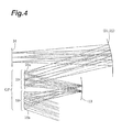
- Fig. 4 is a drawing schematically showing the configuration and action of the optical integrator in the first embodiment.
- the optical integrator OP of the first embodiment is comprised of a first fly eye mirror 18 consisting of a plurality of first concave reflector elements (first mirror elements; first focusing elements) 18a arranged in parallel; a second fly eye mirror 20 consisting of a plurality of second concave reflector elements (second mirror elements; second focusing elements) 20a arranged in parallel so as to correspond to the plurality of first concave reflector elements 18a; and a concave reflecting mirror (relay mirror) 19 as a relay optical system disposed in the optical path between the pair of fly eye mirrors 18 and 20.
- a first fly eye mirror 18 consisting of a plurality of first concave reflector elements (first mirror elements; first focusing elements) 18a arranged in parallel
- a second fly eye mirror 20 consisting of a plurality of second concave reflector elements (second mirror elements; second focusing elements) 20a arranged in
- the condenser optical system (21, 22) is illustrated as a single concave reflecting mirror, and the concave reflector elements 18a, 20a forming the pair of fly eye mirrors 18, 20 are illustrated only by a number much smaller than the actual number.
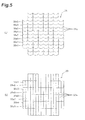
- the first fly eye mirror 18, as shown in Fig. 5(a), is comprised of first concave reflector elements 18a of an arcuate outer shape arranged vertically and horizontally and densely.
- the second fly eye mirror 20, as shown in Fig. 5(b) is comprised of second concave reflector elements 20a of a rectangular outer shape arranged vertically and horizontally and almost densely.
- the first concave reflector elements 18a and the second concave reflector elements 20a have their respective optical surfaces (reflecting surfaces) of the outer shapes different from each other.
- the pattern of parallel arrangement of the first concave reflector elements 18a is different from the pattern of parallel arrangement of the second concave reflector elements 20a, which will be described later.
- the contour of the first fly eye mirror 18, when viewed from the traveling direction of light is a shape close to a circular shape in order to enhance illumination efficiency (cf. Fig. 5(a)).
- each of the first concave reflector elements 18a, the second concave reflector elements 20a, and the concave reflecting mirror 19 is constructed as a toric mirror.
- the focal length in the direction parallel to the plane of Fig. 4 is different from the focal length in the direction normal to the plane of Fig. 4.
- the concave reflecting mirror 19 as a relay optical system has mutually different focal lengths in the direction parallel to the plane of Fig. 4 and in the direction normal to the plane of Fig. 4, and thus has object-image distances different from each other in these two directions eventually.
- the optical integrator OP of the first embodiment when a parallel beam is incident to the first fly eye mirror 18, as indicated by solid lines in the drawing, the incident light is subjected to wavefront dividing by the individual first concave reflector elements 18a. A beam reflected by each first concave reflector element 18a is focused once, and thereafter travels via the concave reflecting mirror 19 as a relay optical system to be focused at a point on or near a reflecting surface of a corresponding second concave reflector element 20a. In this manner, a substantial surface illuminant is formed on or near the exit surface of the optical integrator OP.
- first concave reflector elements 18a are constructed as toric mirrors as described above, a position where a beam reflected by a first concave reflector element 18a is focused at a point in a plane parallel to the plane of Fig. 4 is different from a position where the beam is focused at a point in a plane normal to the plane of Fig. 4.
- Beams each of which is focused at a point on or near a reflecting surface of a second concave reflector element 20a i.e., beams from respective light sources forming the substantial surface illuminant are guided via the condenser optical system (21, 22) to illuminate the arcuate illumination region on the mask M as a surface to be illuminated, in a superimposed manner.
- the concave reflecting mirror (relay optical system) 19 refocuses a beam focused via one of the first concave reflector elements 18a, on or near a corresponding second concave reflector element 20a so as to establish an imaging relation of one-to-one correspondence between one of the first concave reflector elements 18a forming the first fly eye mirror 18 and one of the second concave reflector elements 20a forming the second fly eye mirror 20.
- first concave reflector elements 18a1-18a8 in the leftmost column in Fig. 5(a); the four upper first concave reflector elements 18a1-18a4 correspond to four second concave reflector elements 20a1-20a4, respectively, in the leftmost column in Fig. 5(b).
- the four lower first concave reflector elements 18a5-18a8 correspond to four second concave reflector elements 20a5-20a8, respectively, in the second column from the left in Fig. 5(b).
- the first concave reflector elements 18a in one column in the first fly eye mirror 18 correspond to the second concave reflector elements 20a in two columns in the second fly eye mirror 20 as described above; therefore, the first fly eye mirror 18 is of 8-column structure, while the second fly eye mirror 20 is of 16-column structure.
- each first concave reflector element 18a rays diverging from a point on a reflecting surface of each first concave reflector element 18a, as indicated by dashed lines in the drawing, are guided via the concave reflecting mirror 19 as a relay optical system to be focused once, and thereafter are incident to a corresponding second concave reflector element 20a.
- the concave reflecting mirror 19 is also constructed as a toric mirror as described above, a position where a beam reflected by the concave reflecting mirror 19 is focused at a point in a plane parallel to the plane of Fig. 4 is different from a position where the beam is focused at a point in a plane normal to the plane of Fig. 4.
- each second concave reflector element 20a is guided via the condenser optical system (21, 22) to be focused at a point in the arcuate illumination region on the mask M.
- each of the reflecting surfaces of all the first concave reflector elements 18a forming the first fly eye mirror 18 is arranged so as to be conjugate with the pattern surface of the mask M.
- the reason why the first concave reflector elements 18a forming the first fly eye mirror 18 have the arcuate outer shape is that the arcuate illumination region can efficiently be illuminated on the mask M.
- the reason why the second concave reflector elements 20a forming the second fly eye mirror 20 have the rectangular outer shape vertically long is that the light source images formed on or near the reflecting surfaces of the second concave reflector elements 20a are of a vertically long elliptic shape. When the etendue of the light source is close to that of the apparatus, this configuration can improve transmission efficiency of optical energy.
- a preferred configuration is such that a clearance is provided between the second concave reflector elements 20a forming the second fly eye mirror 20, to provide an adjustment margin in positioning of the individual second concave reflector elements 20a, i.e., to enable positional adjustment of the individual second concave reflector elements 20a.
- the concave reflecting mirror 19 as a relay optical system is disposed in the optical path between the first fly eye mirror 18 and the second fly eye mirror 20.
- the concave reflecting mirror (relay optical system) 19 refocuses a light beam focused via one of the first concave reflector elements 18a, on or near a corresponding second concave reflector element 20a so as to establish an imaging relation of one-to-one correspondence between one of the first concave reflector elements 18a forming the first fly eye mirror 18 and one of the second concave reflector elements 20a forming the second fly eye mirror 20.
- the distance between the entrance surface and the exit surface i.e., the distance between the first fly eye mirror 18 and the second fly eye mirror 20 is permitted to be relatively freely set independent of the focal length of the first fly eye mirror 18.
- the first embodiment realizes the optical integrator OP of the wavefront dividing type permitting an arbitrary distance to be set between the entrance surface and the exit surface, for example, without production of aberration and without reduction in reflectance on reflecting films.
- the illumination optical apparatus of the first embodiment is able to illuminate the mask M as a surface to be illuminated, under a desired illumination condition, using the optical integrator OP permitting an arbitrary distance to be set between the entrance surface and the exit surface.
- the exposure apparatus of the first embodiment is able to perform good projection exposure under a good illumination condition, using the illumination optical apparatus for illuminating the mask M as a surface to be illuminated, under a desired illumination condition.
- each of the reflecting surfaces of all the first concave reflector elements 18a forming the first fly eye mirror 18 is set to be conjugate with the pattern surface of the mask M (and with the exposure surface of the wafer W eventually). Therefore, in order to enhance illumination efficiency according to the conventional technology, the first concave reflector elements 18a are required to have an oblong arcuate outer shape similar to the outer shape of the illumination region on the mask M (in turn, the static exposure region ER on the wafer W) (cf. Fig. 3).
- the outer shape of the first fly eye mirror 18, when viewed from the traveling direction of light, is required to have a shape close to a circular shape (cf. Fig. 5(a)) in order to increase the illumination efficiency.
- the first concave reflector elements 18a need to be arranged in parallel by an enough number both in the horizontal direction and in the vertical direction, in order to achieve the required wavefront dividing effect. For this reason, if the outer shape of the first concave reflector elements 18a is set to the oblong arcuate shape similar to the outer shape of the static exposure region ER of the wafer W as in the conventional technology, the number of first concave reflector elements arranged along the transverse direction of the outer shape will become too large (cf. Fig. 12(b) for the second embodiment described later), which will adversely affect the production cost of the first fly eye mirror 18 and, in turn, the production cost of the optical integrator OP.
- each of the first concave reflector elements 18a, the second concave reflector elements 20a, and the concave reflecting mirror 19 is constructed as a toric mirror, and thus the outer shape of the first concave reflector elements 18a can be set to the relatively wide arcuate shape of an aspect ratio different from that of the outer shape of the static exposure region ER of the wafer W.
- the first fly eye mirror 18 of the first embodiment as shown in Fig.
- the number of first concave reflector elements 18a arranged along the transverse direction of the arcuate outer shape is not too large, which can keep the production cost of the first fly eye mirror 18 low and, in turn, the production cost of the optical integrator OP low.
- the light source images formed on or near the reflecting surfaces of the second concave reflector elements 20a are of the vertically long elliptic shape, and the second concave reflector elements 20a forming the second fly eye mirror 20 have the vertically long rectangular outer shape in order to improve the transmission efficiency of optical energy.
- the contour of the second fly eye mirror 20 when viewed from the traveling direction of light, will become extremely thin and long along the longitudinal direction of the second concave reflector elements 20a of the rectangular shape (the vertical direction in Fig. 5(b)).
- the pattern of parallel arrangement of the first concave reflector elements 18a is different from the pattern of parallel arrangement of the second concave reflector elements 20a.
- the first concave reflector elements 18a in one column of the first fly eye mirror 18 correspond to the second concave reflector elements 20a in two columns of the second fly eye mirror 20, the first fly eye mirror 18 is of the 8-column structure, and the second fly eye mirror 20 is of the 16-column structure.
- the contour of the second fly eye mirror 20 viewed from the traveling direction of light, is the shape close to the circular shape as in the case of the first fly eye mirror 18.
- the EUVL exposure apparatus of the first embodiment described above uses the laser plasma light source as a light source for supplying EUV light.
- the light source can be any other adequate light source for supplying EUV light, e.g., a synchrotron (SOR) light source.
- SOR synchrotron
- ⁇ -value NA1/NA2: ratio of the mask-side numerical aperture NA1 of the illumination optical system 2 to the mask-side numerical aperture NA2 of the projection optical system PL
- ⁇ -value NA1/NA2: ratio of the mask-side numerical aperture NA1 of the illumination optical system 2 to the mask-side numerical aperture NA2 of the projection optical system PL
- the controller CR determines whether the ⁇ -value is to be changed, based on the input information from the input device, every time a wafer W is mounted on the wafer stage 7.
- the controller CR determines that the ⁇ -value needs to be changed, it actuates a driver DR1 to replace an aperture stop 24e for circular illumination located near the reflecting surface of the second fly eye mirror 20, with another aperture stop for circular illumination having a different aperture diameter.
- a turret method, a slide method, or the like can be used for the changeover between aperture stops. The following will describe an example in which the turret method is applied to the changeover between aperture stops.
- a turret plate 23 which can be rotated about a predetermined rotation axis 23a by action of the driver DR1.
- the turret plate 23, as shown in Fig. 7, is provided with a plurality of aperture stops 24a-24f (six aperture stops as an example in Fig. 7) different in the shape or size of the aperture portion (light transmitting portion) from each other.
- hatched regions correspond to the aperture portions of the respective aperture stops.
- the aperture stop 24a is an aperture stop for annular illumination having an annular aperture portion 24aa
- aperture stops 24b and 24e are aperture stops for circular illumination having their respective aperture portions 24ba and 24ea of circular shape having different aperture diameters.
- the aperture stop 24c is an aperture stop for quadrupole illumination having four fan-shaped aperture portions 24ca-24cd, and the aperture stop 24d an aperture stop for quadrupole illumination having four circular aperture portions 24da-24dd.
- the aperture stop 24f is an aperture stop for annular illumination having an aperture portion 24fa with an annular ratio different from that of the aperture stop 24a. The definition of the annular ratio, and use of the annular illumination aperture stops 24a, 24f and quadrupole illumination aperture stops 24c, 24d will be described later. It is noted that a variety of modification examples can be contemplated as to the number and arrangement of aperture stops, the shape and size of the aperture portions, etc. in the turret plate 23.
- Fig. 4 exemplifies the configuration in which the first fly eye mirror 18 and the second fly eye mirror 20 are arranged at nearly equal positions along the horizontal direction in the drawing, but the interposition of the relay optical system 19 permits a variety of configuration examples to be realized as to the horizontal positions of the first fly eye mirror 18 and the second fly eye mirror 20 in the horizontal direction in the drawing. Namely, the first fly eye mirror 18 can be located to the right side or to the left side in the drawing of the second fly eye mirror 20, whereby the required space can be secured around the second fly eye mirror 20 (cf. the arrangement in Fig. 1).
- the center of curvature of the reflecting surface of the relay optical system (relay mirror) 19 is present between the first concave reflector elements (first mirror elements) 18a and the relay optical system 19 or between the second concave reflector elements (second mirror elements) 20a and the relay optical system 19.
- the reflecting surface of the relay optical system 19 is a toric surface
- the centers of curvature of the reflecting surface in two mutually orthogonal directions are also preferably present between either one of the first concave reflector elements and the second concave reflector elements, and the relay optical system 19.
- the first embodiment permits such design as to set the focal length of the first fly eye mirror 18 to a small value, as described above, whereby it becomes feasible to set the outer shapes of the first concave reflector elements (first mirror elements) 18a and the second concave reflector elements (second mirror elements) 20a small.
- the first embodiment permits the wavefront-dividing surfaces of the optical integrator OP to be set small, whereby occurrence of illumination unevenness due to change of the ⁇ -value can be suppressed well without need for replacement of the concave reflecting mirror 17 as a collimating mirror.
- a reflective conical axicon system 25 as an annular beam converting unit is provided in a retractable state relative to the illumination optical path between the concave reflecting mirror 17 as a collimating mirror and the first fly eye mirror 18.
- the conical axicon system 25 has a function of converting an EUV beam of a circular cross section into an EUV beam of an annular (ring) cross section.
- the conical axicon system 25 is comprised of the following members in the order of incidence of light: a first reflecting member 25a having a reflecting surface 25aa of a convex conical shape; and a second reflecting member 25b (the main body of which is omitted from the illustration in order to clarify the drawing) having a reflecting surface 25ba of an annular conical shape which is obtained by cutting an annular, rotationally symmetric region away from a concave conical surface complementary to the reflecting surface 25aa of the first reflecting member 25a.
- At least one of the first reflecting member 25a and the second reflecting member 25b is arranged movable along the optical axis AX, whereby the distance is variable between the reflecting surface 25aa of the first reflecting member 25a and the reflecting surface 25ba of the second reflecting member 25b.
- the resulting beam becomes an EUV beam La2 of an annular shape having a larger outside diameter and inside diameter, which is guided to the first fly eye mirror 18 of the optical integrator OP.
- an optical intensity distribution (secondary light source) of an annular shape is formed on the illumination pupil (near the exit surface of the second fly eye mirror 20) by action of the reflective conical axicon system 25.
- the outside diameter (inside diameter) of the secondary light source of annular shape will change while keeping the width of the secondary light source of the annular shape (half of the difference between the outside diameter and inside diameter of the annular secondary light source) constant.
- the annular ratio (inside diameter/outside diameter) and size (outside diameter) of the secondary light source of annular shape varies through action of the conical axicon system 25.
- the insertion/retraction of the conical axicon system 25 relative to the illumination optical path, and the relative movement between the first reflecting member 25a and the second reflecting member 25b along the illumination optical path are implemented by a driver DR2 which operates based on a command from the controller CR.
- the controller CR selects one of "first annular illumination,” “second annular illumination,” “first normal circular illumination,” “second normal circular illumination,” “first quadrupole illumination,” and “second quadrupole illumination,” based on input information from an input device (not shown) for inputting necessary information for selection of an illumination condition on the mask M or on the wafer W.
- the input device is a device for inputting exposure information about exposure conditions for respective wafers successively mounted by an unrepresented conveying device (a conveyance map of wafers including exposure information, or the like) according to fineness of patterns to be transferred onto the wafers W and a process of patterns to be transferred onto the wafers W, and mount information about various masks successively mounted on the mask stage 5.
- the secondary light source is formed in an annular shape on the illumination pupil (near the exit surface of the second fly eye mirror 20) to illuminate the reflective mask M and wafer W obliquely with EUV light, thereby improving the original resolving power and depth of focus of the projection optical system PL.
- the "quadrupole illumination (more generally, multi-pole illumination)” is defined as follows: the secondary light source formed on the illumination pupil consists of four (multiple in general) discrete off-axis light sources decentered by a predetermined distance from the center of the secondary light source, to illuminate the reflective mask M and wafer W obliquely with EUV light, thereby improving the original resolving power and depth of focus of the projection optical system PL.
- the "normal circular illumination” is illumination in which the shape of the secondary light source formed on the illumination pupil is approximately circular so that the reflective mask M and wafer W are illuminated under an optimal ⁇ -value.
- the controller CR selects "first normal circular illumination” or “second normal circular illumination,” based on the input information from the input device.
- the difference between “first normal circular illumination” and “second normal circular illumination” is a difference of ⁇ -value.
- the controller CR selects "first normal circular illumination,” it drives the driver DR1 to rotate the turret plate 23 so that the aperture stop 24e is located at the position of the secondary light source (substantial surface illuminant consisting of a number of light sources) formed on the illumination pupil (near the exit surface of the second fly eye mirror 20).
- the controller CR changes an aperture diameter of a variable aperture stop (not shown) in the projection optical system PL as occasion may demand.
- the controller CR actuates the driver DR2 to retract the conical axicon system 25 from the illumination optical path.
- the controller CR When the controller CR selects "second normal circular illumination,” it drives the driver DR1 to rotate the turret plate 23 so that the aperture stop 24b is located at the position of the secondary light source formed on the illumination pupil. At the same time as it, the controller CR changes the aperture diameter of the variable aperture stop (not shown) in the projection optical system PL as occasion may demand. At this time, if the conical axicon system 25 is set in the illumination optical path, the controller CR actuates the driver DR2 to retract the conical axicon system 25 from the illumination optical path.
- the pattern of the reflective mask M When the pattern of the reflective mask M is illuminated with EUV light in the above setting condition, the pattern of the reflective mask M can be projected through the projection optical system PL onto the photosensitive substrate (wafer) W under an appropriate condition of "second normal circular illumination" (a ⁇ -value larger than that in the first normal circular illumination).
- the controller CR selects one of "first annular illumination,” “second annular illumination,” “first quadrupole illumination,” and “second quadrupole illumination,” based on the input information from the input device.
- first annular illumination and “second annular illumination” are different in the annular ratio of the secondary light source of the annular shape from each other.
- the “first quadrupole illumination” and “second quadrupole illumination” are different mainly in the shape of the surface illuminant of each pole. Namely, the secondary light source in “first quadrupole illumination” consists of four fan-shaped regions, and the secondary light source in “second quadrupole illumination” consists of four circular regions.
- the controller CR drives the driver DR1 to rotate the turret plate 23 so that the aperture stop 24a is located at the position of the secondary light source formed on the illumination pupil.
- the controller CR drives the driver DR1 to rotate the turret plate 23 so that the aperture stop 24f is located at the position of the secondary light source formed on the illumination pupil.
- the controller CR drives the driver DR1 to rotate the turret plate 23 so that the aperture stop 24c is located at the position of the secondary light source formed on the illumination pupil.
- the controller CR drives the driver DR1 to rotate the turret plate 23 so that the aperture stop 24d is located at the position of the secondary light source formed on the illumination pupil.
- the controller CR changes the aperture diameter of the variable aperture stop (not shown) in the projection optical system PL as occasion may demand. Then the controller CR drives the driver DR2 to set the conical axicon system 25 as an annular beam converting unit on the illumination optical path and to adjust the conical axicon system 25. First, if the conical axicon system 25 is not set in the illumination optical path, the controller CR drives the driver DR2 to set the conical axicon system 25 at a predetermined position in the illumination optical path.
- the controller CR drives the driver DR2 to change the relative distance between the two reflecting members (25a, 25b) in the conical axicon system 25 so that the annular beam is efficiently guided to the aperture portion of one aperture stop among the four aperture stops (24a, 24c, 24d, 24f) set at the position of the secondary light source formed on the illumination pupil.
- This enables the conical axicon system 25 to convert the incident beam of nearly circular shape into an annular shape having an appropriate annular ratio.
- the secondary light source having an appropriate annular ratio according to each aperture portion among the four aperture stops (24a, 24c, 24d, 24f) is formed on the illumination pupil, whereby the mask M and wafer W can be illuminated by off-axis illumination at high illumination efficiency.
- the illumination state can worsen with occurrence of illumination unevenness or the like in the arcuate illumination region (static exposure region ER) formed on the wafer W or on the mask M.
- the wavefront dividing surfaces of the optical integrator OP can be set small in the first embodiment as described above, whereby occurrence of illumination unevenness due to the changeover of the aperture stop (24a-24f) can be suppressed well without need for replacement of the concave reflecting mirror 17 as a collimating mirror.
- the above description concerned the configuration wherein the information such as the illumination condition was fed through the input device to the controller CR, but it is also possible to adopt a configuration wherein there is a detector for reading information on the reflective mask M.
- information about an illumination method e.g., a barcode or the like, is recorded outside a circuit pattern region of the mask M.
- the detector reads the information about the illumination condition and transmits it to the controller CR.
- the controller CR controls the drivers (DR1, DR2), based on the information about the illumination condition.
- a quadrangular pyramid axicon system is comprised, for example, of a first reflecting member having a reflecting surface of a convex quadrangular pyramid shape, and a second reflecting member having a reflecting surface of an annular, quadrangular pyramid shape obtained by cutting a rotationally symmetric region of annular shape away from a concave quadrangular pyramid surface complementary to the reflecting surface of the first reflecting member.
- an optical intensity distribution (secondary light source) of quadrupole shape is formed on the circular pupil plane (indicated by a dashed line in the drawing) by the action of the quadrangular pyramid axicon system.
- the outside diameter (inside diameter) of the secondary light source of quadrupole shape varies while keeping the width of the secondary light source of quadrupole shape (half of a difference between a diameter (outside diameter) of a circle circumscribing the secondary light source of quadrupole shape and a diameter (inside diameter) of a circle inscribing the secondary light source) constant.
- the annular ratio (inside diameter/outside diameter) and size (outside diameter) of the secondary light source of quadrupole shape varies through action of the quadrangular pyramid axicon system.
- a secondary light source of a dipole shape can also be formed by means of a reflective V-groove axicon system (not shown) as a dipole beam converting unit.
- the V-groove axicon system is comprised, for example, of a first reflecting member having a reflecting surface of a convex V-shape, and a second reflecting member having a reflecting surface of an annular V-shape obtained by cutting a rotationally symmetric region of an annular shape away from a concave V-shape complementary to the reflecting surface of the first reflecting member.
- an optical intensity distribution (secondary light source) of dipole shape is formed on the circular pupil plane (indicated by a dashed line in the drawing) by the action of the V-groove axicon system.
- the aperture stop was located at the position of the secondary light source formed on the illumination pupil.
- the installation of the aperture stop can be omitted depending upon circumstances.
- the first embodiment permits the wavefront dividing surfaces of the optical integrator OP to be set small and the optical intensity distribution (secondary light source) of almost desired shape is thus formed on the illumination pupil by means of the conical axicon system, rectangular pyramid axicon system, V-groove axicon system, or the like.
- the aperture stop is located at the position of the secondary light source formed on the illumination pupil, in order to suppress influence of flare.
- the above first embodiment showed the example in which the aperture stops (24b, 24e) with different aperture diameters to vary the ⁇ -value were set in the illumination optical path, but it is also possible to adopt a configuration wherein a plurality of collimating mirrors 17 with mutually different focal lengths are arranged replaceable, in order to improve the illumination efficiency.
- the illumination optical system 2 of the first embodiment is arranged as follows: a multilayer film for reflecting EUV light is provided, for example, on the reflecting surface of the concave reflecting mirror 17, the reflecting surface of each first concave reflector element (first mirror element) 18a in the first fly eye mirror 18, the reflecting surface of each second concave reflector element (second mirror element) 20a in the second fly eye mirror 20, and the reflecting surface of the concave reflecting mirror 19.
- the incidence angle of EUV light incident to a reflecting surface is desirably kept at about 10°, in order to secure a required reflectance on the reflecting surface consisting of an ordinary multilayer film.
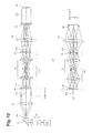
- Fig. 10 is a drawing schematically showing a configuration of an exposure apparatus according to the second embodiment of the present invention.
- a Y-axis is set along a direction of the optical axis AX of the projection optical system PL, i.e., along a direction of a normal to the plane of wafer W as a photosensitive substrate, a Z-axis along a direction parallel to the plane of Fig. 10 in the plane of wafer W, and an X-axis along a direction perpendicular to the plane of Fig. 10 in the plane of wafer W.
- the present invention is applied to the exposure apparatus, for example, with an ArF excimer laser light source for supplying light at the wavelength of 193 nm or with a KrF excimer laser light source for supplying light at the wavelength of 248 nm.
- the exposure apparatus of the second embodiment has a light source 31 for supplying exposure light (illumination light).
- a light source 31 for supplying exposure light (illumination light).
- Light emitted from the light source 31 such as the ArF excimer laser light source or the KrF excimer laser light source is guided through a shaping optical system 32 to be expanded into a beam of a required sectional shape, and thereafter the light is reflected by a path bending mirror 33 to enter a fly eye lens 34.
- the beam incident to the fly eye lens 34 is two-dimensionally divided by a number of lens elements to form a number of light sources on or near the rear focal plane thereof.
- the optical integrator OP is composed of a pair of fly eye members 36 and 37, and a relay optical system 38 disposed in the optical path between them, the detailed configuration and action of which will be described later.
- the beams incident to the optical integrator OP (36-38) form a substantial surface illuminant (secondary light source) of a predetermined shape near the second fly eye member, i.e., near the exit surface of the optical integrator OP.
- the substantial surface illuminant is formed at or near the position of the exit pupil of the illumination optical system (32-39), i.e., on or near a plane optically conjugate with the entrance pupil of the projection optical system PL.
- Light from the substantial surface illuminant is guided through a condenser optical system 39 as a light-guiding optical system to illuminate a mask M with a predetermined pattern in a superimposed manner.
- a pattern to be transformed is formed in the mask M, and a pattern region of a rectangular shape (slit shape) having longer sides along the X-direction and shorter sides along the Z-direction is illuminated in the entire pattern region.
- a beam passing through the pattern of mask M travels through the projection optical system PL to form a pattern image of the mask M on a wafer W as a photosensitive substrate.
- the pattern image is also formed in a static exposure region (effective exposure region) of a rectangular shape having longer sides along the X-direction and shorter sides along the Z-direction on the wafer W, so as to optically correspond to the illumination region of the rectangular shape on the mask M.
- the mask M and wafer W are synchronously moved (to scan) along the Z-direction (scanning direction) in the plane (XZ plane) perpendicular to the optical axis AX of the projection optical system PL according to the so-called step-and-scan method, as shown in Fig.
- the mask pattern is formed by scanning exposure in a shot area (exposure region) SR having a width equal to the X-directional size of the static exposure region ER and a length according to a scanning distance (movement amount) of the wafer W, on the wafer W.
- the optical integrator OP of the second embodiment is composed of the first fly eye member 36 consisting of a plurality of first positive lens elements (first focusing elements) 36a arranged in parallel, the second fly eye member 37 consisting of a plurality of second positive lens elements (second focusing elements) 37a arranged in parallel so as to correspond to the plurality of first positive lens elements 36a, and the relay optical system 38 disposed in the optical path between the pair of fly eye members 36 and 37.
- the positive lens (positive single lens) elements 36a, 37a constituting the pair of fly eye members 36, 37 are illustrated by a number much smaller than the actual number.
- the first fly eye member 36 is constructed by arranging the first positive lens elements 36a of rectangular outer shape vertically and horizontally and densely.
- the second fly eye member 37 is also constructed by arranging the second positive lens elements 37a of rectangular outer shape vertically and horizontally and densely, according to a pattern of parallel arrangement similar to that of the first fly eye member 36. Since the sectional shape of the beam incident to the optical integrator OP is nearly circular, the contour shape of the first fly eye member 36, when viewed from the traveling direction of light, is of a shape close to a circular shape in order to enhance the illumination efficiency (cf. Fig. 12(a)). Fig.
- the relay optical system 38 was composed of three, positive, negative, and positive lenses, but the relay optical system 38 can also be constructed of a positive single lens. Furthermore, the relay optical system can also be constructed of a plurality of lens units, e.g., positive, negative, and positive lens units.
- each of the first positive lens elements 36a, the second positive lens elements 37a, and the relay optical system 38 is constructed as a toric lens. Namely, in the first positive lens elements 36a and the second positive lens elements 37a, the focal length about the YZ plane is different from the focal length about the XY plane.
- the relay optical system 38 has mutually different focal lengths on the YZ plane and on the XY plane, and thus has mutually different object-image distances in these two directions.
- the optical integrator OP of the second embodiment when the parallel beam is incident to the first fly eye member 37, the incident beam is subject to wavefront dividing by the individual first positive lens elements 36a, as indicated by solid lines in Fig. 10. Then a beam through each first positive lens element 36a is focused once and thereafter travels through the relay optical system 38 to be focused at a point on or near a corresponding second positive lens element 37a. In this manner, a substantial surface illuminant is formed on or near the exit surface of the optical integrator OP.
- each first positive lens element 36a is constructed as a toric lens as described above, a position where a beam through a first positive lens element 36a is focused at a point in the YZ plane is different from a position where the beam is focused at a point in the XZ plane.
- Beams each focused at a point on or near each second positive lens element 37a, i.e., beams from respective light sources constituting the substantial surface illuminant are guided through the condenser optical system 39 to illuminate the rectangular illumination region on the mask M as a surface to be illuminated, in a superimposed manner.
- the relay optical system 38 refocuses a beam focused via one of the first positive lens elements 36a, on or near a corresponding second positive lens element 37a so as to establish an imaging relation of one-to-one correspondence between one of the first positive lens elements 36a forming the first fly eye member 36 and one of the second positive lens elements 37a forming the second fly eye member 37.
- rays diverging from a point on each first positive lens element 36a are guided through the relay optical system 38 to be focused once, as indicated by dashed lines in Fig. 5, and thereafter are incident to each corresponding second positive lens element 37a.
- the relay optical system 38 is also constructed as a toric lens (toric optical system) as described above, a position where the beam through the relay optical system 38 is focused at a point in the YZ plane is different from a position where the beam is focused at a point in the XY plane.
- the beams passing through the respective second positive lens elements 37a are guided through the condenser optical system 39 to be focused at a point in the rectangular illumination region on the mask M.
- each of all the first positive lens elements 36a forming the first fly eye member 36 is arranged so as to be conjugate with the pattern surface of the mask M. The reason why the first positive lens elements 36a forming the first fly eye member 36 have the rectangular outer shape is that the rectangular illumination region can efficiently be illuminated on the mask M.
- the relay optical system 38 is disposed in the optical path between the first fly eye member 36 and the second fly eye member 37.
- the relay optical system 38 refocuses a light beam focused via one of the first positive lens elements 36a, on or near a corresponding second positive lens element 37a so as to establish an imaging relation of one-to-one correspondence between one of the first positive lens elements 36a forming the first fly eye member 36 and one of the second positive lens elements 37a forming the second fly eye member 37.
- the second embodiment also permits the distance between the first fly eye member 36 and the second fly eye member 37 to be relatively freely set independent of the focal length of the first fly eye member 36.
- the first positive lens elements 36a forming the first fly eye member 36 are set each to be conjugate with the pattern surface of the mask M (and with the exposure surface of the wafer W eventually). Therefore, in order to enhance the illumination efficiency according to the conventional technology, the first positive lens elements 36a are required to have an oblong rectangular outer shape similar to the outer shape of the illumination region of the mask M (and the static exposure region ER of the wafer W eventually) (cf. Fig. 11). On the other hand, since the sectional shape of the beam incident to the optical integrator OP is nearly circular as described above, the contour of the first fly eye member 36, when viewed from the traveling direction of light, needs to be a shape close to the circular shape (cf. Fig. 12(a)) in order to enhance the illumination efficiency.
- the first positive lens elements 36a need to be arranged in parallel by an enough number both in the horizontal direction and in the vertical direction, in order to achieve the required wavefront dividing effect. For this reason, if the outer shape of the first positive lens elements 36a is set to an oblong rectangular shape similar to the outer shape of the static exposure region ER of the wafer W as in the conventional technology, the number of first positive lens elements arranged in the transverse direction of the outer shape will be too large (cf. Fig. 12(b)), which will adversely affect the production cost of the first fly eye member 36 and, in turn, the production cost of the optical integrator OP.
- each of the first positive lens elements 36a, the second positive lens elements 37a, and the relay optical system 38 is constructed as a toric lens as described above, the outer shape of the first positive lens elements 36a can be set to a rectangular shape close to a square in an aspect ratio different from that of the outer shape of the static exposure region ER in the wafer W.
- the number of first positive lens elements 36a arranged along the transverse direction of the rectangular outer shape is not too large, which can keep down the production cost of the first fly eye member 36 and, in turn, the production cost of the optical integrator OP.
- the above-described second embodiment adopted the scanning exposure of the mask pattern in each shot area SR performed by synchronously moving the mask M and the wafer W relative to the projection optical system PL according to the step-and-scan method.
- the condenser optical system 39 focuses the light from the secondary light source (the substantial surface illuminant formed near the exit surface of the optical integrator OP) to illuminate the mask M in a superimposed manner.
- the condenser optical system 39 focuses the light from the secondary light source to illuminate the illumination field stop in a superimposed manner, and the imaging optical system forms an image of an aperture portion (light transmitting portion) of the illumination field stop on the mask M.
- the exposure apparatus can be used to produce micro devices (semiconductor devices, image pickup devices, liquid-crystal display devices, thin-film magnetic heads, etc.) by illuminating a mask (reticle) by the illumination optical apparatus (illumination step) and exposing a photosensitive substrate to a pattern for printing formed on the mask, by the projection optical system (exposure step).
- a mask reticle
- illumination optical apparatus illumination step
- exposure step exposing a photosensitive substrate to a pattern for printing formed on the mask
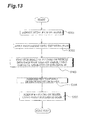
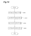
- exposure step An example of a method of fabricating semiconductor devices as micro devices by forming a predetermined circuit pattern on a wafer or the like as a photosensitive substrate with the use of the exposure apparatus of the above embodiment will be described below with reference to the flowchart of Fig. 13.
- the first step 301 in Fig. 13 is to deposit a metal film on each of wafers in one lot.
- the next step 302 is to apply a photoresist onto the metal film on each wafer in the lot.
- the subsequent step 303 is to project and print an image of a pattern on a mask into each shot area on each wafer in the lot through the projection optical system, using the exposure apparatus of the above embodiments.
- the next step 304 is to perform development of the photoresist on each wafer in the lot, and the subsequent step 305 is to perform etching with the resist pattern as a mask on each wafer in the lot to form a circuit pattern corresponding to the pattern on the mask, in each shot area on each wafer.
- circuit patterns of upper layers are further formed and other steps are carried out to fabricate devices such as semiconductor devices.
- the above-described semiconductor device fabrication method permits us to obtain semiconductor devices with extremely fine circuit patterns at high throughput.
- a pattern forming step 401 is to execute a so-called photolithography step of transferring and printing a pattern of a mask onto a photosensitive substrate (a glass substrate coated with a resist, or the like) with the use of the exposure apparatus of the above embodiments.
- This photolithography step results in forming the predetermined pattern including a number of electrodes and others on the photosensitive substrate.
- the exposed substrate is subjected to steps such as a development step, an etching step, and a resist removing step, whereby the predetermined pattern is formed on the substrate, followed by the next color filter forming step 402.
- the next color filter forming step 402 is to form a color filter in which a number of sets of three dots corresponding to R (Red), G (Green), and B (Blue) are arrayed in a matrix or in which a plurality of sets of three stripes of R, G, and B are arrayed in a direction of horizontal scan lines.
- a cell assembling step 403 is carried out.
- the cell assembling step 403 is to assemble a liquid crystal panel (liquid crystal cell), using the substrate with the predetermined pattern obtained by the pattern forming step 401, the color filter obtained by the color filter forming step 402, and so on.
- a liquid crystal is poured into between the substrate with the predetermined, pattern obtained by the pattern forming step 401 and the color filter obtained by the color filter forming step 402, to fabricate the liquid crystal panel (liquid crystal cell).
- the subsequent module assembling step 404 is to mount such components as an electric circuit and a backlight for implementing a display operation of the assembled liquid crystal panel (liquid crystal cell), to complete a liquid-crystal display device.
- the method of fabricating the liquid-crystal display device as described above permits us to obtain the liquid-crystal display devices with extremely fine circuit patterns at high throughput.
- the foregoing embodiments showed the examples in which the present invention was applied to the optical integrators for uniformizing the illumination light for illuminating the surface to be illuminated in the illumination optical apparatus, but, without having to be limited to this, the present invention can also be applied to the general optical integrators of the wavefront dividing type.
- the foregoing embodiments were the examples in which the present invention was applied to the illumination optical apparatus for illuminating the mask in the exposure apparatus, but, without having to be limited to this, the present invention can also be applied to the general illumination optical apparatus for illuminating a surface to be illuminated, except for masks.
Landscapes
- Physics & Mathematics (AREA)
- General Physics & Mathematics (AREA)
- Optics & Photonics (AREA)
- Exposure And Positioning Against Photoresist Photosensitive Materials (AREA)
- Exposure Of Semiconductors, Excluding Electron Or Ion Beam Exposure (AREA)
- Lenses (AREA)
Applications Claiming Priority (2)
| Application Number | Priority Date | Filing Date | Title |
|---|---|---|---|
| JP2005027528 | 2005-02-03 | ||
| PCT/JP2006/301112 WO2006082738A1 (ja) | 2005-02-03 | 2006-01-25 | オプティカルインテグレータ、照明光学装置、露光装置、および露光方法 |
Publications (2)
| Publication Number | Publication Date |
|---|---|
| EP1811547A1 true EP1811547A1 (de) | 2007-07-25 |
| EP1811547A4 EP1811547A4 (de) | 2010-06-02 |
Family
ID=36777126
Family Applications (1)
| Application Number | Title | Priority Date | Filing Date |
|---|---|---|---|
| EP06712307A Withdrawn EP1811547A4 (de) | 2005-02-03 | 2006-01-25 | Optischer integrierer, optische beleuchtungsvorrichtung, belichtungsvorrichtung und belichtungsverfahren |
Country Status (8)
| Country | Link |
|---|---|
| US (1) | US7471456B2 (de) |
| EP (1) | EP1811547A4 (de) |
| JP (1) | JPWO2006082738A1 (de) |
| KR (1) | KR20070100964A (de) |
| CN (1) | CN101069267A (de) |
| IL (1) | IL182857A0 (de) |
| TW (1) | TW200629007A (de) |
| WO (1) | WO2006082738A1 (de) |
Cited By (8)
| Publication number | Priority date | Publication date | Assignee | Title |
|---|---|---|---|---|
| WO2008149178A1 (en) * | 2007-06-07 | 2008-12-11 | Carl Zeiss Smt Ag | Catoptric illumination system for microlithography tool |
| WO2010037453A1 (en) * | 2008-09-30 | 2010-04-08 | Carl Zeiss Smt Ag | Field facet mirror for use in an illumination optics of a projection exposure apparatus for euv microlithography |
| NL2008048A (en) * | 2011-01-01 | 2012-07-03 | Canon Kk | Illumination optical system, exposure apparatus, and method of manufacturing device. |
| CN102596126A (zh) * | 2009-07-29 | 2012-07-18 | 爱尔康蓝斯克斯股份有限公司 | 用于眼科手术激光的光学系统 |
| WO2013007731A1 (en) * | 2011-07-11 | 2013-01-17 | Carl Zeiss Smt Gmbh | Illumination optical unit for projection lithography |
| WO2013156278A1 (en) * | 2012-04-16 | 2013-10-24 | Carl Zeiss Smt Gmbh | Optical system of a microlithographic projection exposure apparatus |
| DE102012010093A1 (de) | 2012-05-23 | 2013-11-28 | Carl Zeiss Smt Gmbh | Facettenspiegel |
| CN113625458A (zh) * | 2021-09-13 | 2021-11-09 | 北京理工大学 | 双共焦反射式变倍扩束镜 |
Families Citing this family (53)
| Publication number | Priority date | Publication date | Assignee | Title |
|---|---|---|---|---|
| EP1930771A1 (de) * | 2006-12-04 | 2008-06-11 | Carl Zeiss SMT AG | Projektionsobjektive mit Spiegelelementen mit Reflexbeschichtungen |
| US20090040493A1 (en) * | 2007-08-09 | 2009-02-12 | Hideki Komatsuda | Illumination optical system, illumination optical apparatus, exposure apparatus, and device manufacturing method |
| DE102007041004A1 (de) | 2007-08-29 | 2009-03-05 | Carl Zeiss Smt Ag | Beleuchtungsoptik für die EUV-Mikrolithografie |
| WO2009124595A1 (en) * | 2008-04-11 | 2009-10-15 | Carl Zeiss Smt Ag | Optical aperture device |
| DE102008049585A1 (de) * | 2008-09-30 | 2010-04-08 | Carl Zeiss Smt Ag | Feldfacettenspiegel zum Einsatz in einer Beleuchtungsoptik einer Projektionsbelichtungsanlage für die EUV-Mikrolithographie |
| US8264666B2 (en) * | 2009-03-13 | 2012-09-11 | Nikon Corporation | Exposure apparatus, exposure method, and method of manufacturing device |
| WO2011065374A1 (ja) * | 2009-11-24 | 2011-06-03 | 株式会社ニコン | 結像光学系、露光装置、およびデバイス製造方法 |
| DE102009047179B8 (de) * | 2009-11-26 | 2016-08-18 | Carl Zeiss Smt Gmbh | Projektionsobjektiv |
| US9703204B2 (en) | 2010-04-02 | 2017-07-11 | Nikon Corporation | Light source apparatus, optical apparatus, exposure apparatus, device manufacturing method, illuminating method, exposure method, and method for manufacturing optical apparatus |
| DE102012209132A1 (de) * | 2012-05-31 | 2013-12-05 | Carl Zeiss Smt Gmbh | Beleuchtungsoptik für die Projektionslithographie |
| WO2014079478A1 (en) | 2012-11-20 | 2014-05-30 | Light In Light Srl | High speed laser processing of transparent materials |
| EP2754524B1 (de) | 2013-01-15 | 2015-11-25 | Corning Laser Technologies GmbH | Verfahren und Vorrichtung zum laserbasierten Bearbeiten von flächigen Substraten, d.h. Wafer oder Glaselement, unter Verwendung einer Laserstrahlbrennlinie |
| EP2781296B1 (de) | 2013-03-21 | 2020-10-21 | Corning Laser Technologies GmbH | Vorrichtung und verfahren zum ausschneiden von konturen aus flächigen substraten mittels laser |
| DE102013218132A1 (de) * | 2013-09-11 | 2015-03-12 | Carl Zeiss Smt Gmbh | Kollektor |
| US9701563B2 (en) | 2013-12-17 | 2017-07-11 | Corning Incorporated | Laser cut composite glass article and method of cutting |
| US10293436B2 (en) | 2013-12-17 | 2019-05-21 | Corning Incorporated | Method for rapid laser drilling of holes in glass and products made therefrom |
| US11556039B2 (en) | 2013-12-17 | 2023-01-17 | Corning Incorporated | Electrochromic coated glass articles and methods for laser processing the same |
| US9850160B2 (en) | 2013-12-17 | 2017-12-26 | Corning Incorporated | Laser cutting of display glass compositions |
| US20150165560A1 (en) | 2013-12-17 | 2015-06-18 | Corning Incorporated | Laser processing of slots and holes |
| US9676167B2 (en) | 2013-12-17 | 2017-06-13 | Corning Incorporated | Laser processing of sapphire substrate and related applications |
| US9815730B2 (en) | 2013-12-17 | 2017-11-14 | Corning Incorporated | Processing 3D shaped transparent brittle substrate |
| US10442719B2 (en) | 2013-12-17 | 2019-10-15 | Corning Incorporated | Edge chamfering methods |
| KR102445217B1 (ko) | 2014-07-08 | 2022-09-20 | 코닝 인코포레이티드 | 재료를 레이저 가공하는 방법 및 장치 |
| LT3169477T (lt) * | 2014-07-14 | 2020-05-25 | Corning Incorporated | Skaidrių medžiagų apdorojimo sistema ir būdas, naudojant lazerio pluošto židinio linijas, kurių ilgis ir skersmuo yra reguliuojami |
| EP3536440A1 (de) | 2014-07-14 | 2019-09-11 | Corning Incorporated | Glasartikel mit einem defektweg |
| WO2016010949A1 (en) | 2014-07-14 | 2016-01-21 | Corning Incorporated | Method and system for forming perforations |
| WO2016010991A1 (en) | 2014-07-14 | 2016-01-21 | Corning Incorporated | Interface block; system for and method of cutting a substrate being transparent within a range of wavelengths using such interface block |
| US10047001B2 (en) | 2014-12-04 | 2018-08-14 | Corning Incorporated | Glass cutting systems and methods using non-diffracting laser beams |
| JP2018507154A (ja) | 2015-01-12 | 2018-03-15 | コーニング インコーポレイテッド | マルチフォトン吸収方法を用いた熱強化基板のレーザー切断 |
| KR102601220B1 (ko) * | 2015-03-02 | 2023-11-09 | 에이에스엠엘 네델란즈 비.브이. | 방사선 시스템 |
| WO2016154284A1 (en) | 2015-03-24 | 2016-09-29 | Corning Incorporated | Laser cutting and processing of display glass compositions |
| CN107666983B (zh) | 2015-03-27 | 2020-10-02 | 康宁股份有限公司 | 可透气窗及其制造方法 |
| KR102499697B1 (ko) | 2015-07-10 | 2023-02-14 | 코닝 인코포레이티드 | 유연한 기판 시트에서의 홀의 연속 제조 방법 및 이에 관한 물품 |
| KR102405144B1 (ko) | 2016-05-06 | 2022-06-07 | 코닝 인코포레이티드 | 투명 기판들로부터의 윤곽 형상들의 레이저 절단 및 제거 |
| US10410883B2 (en) | 2016-06-01 | 2019-09-10 | Corning Incorporated | Articles and methods of forming vias in substrates |
| US10794679B2 (en) | 2016-06-29 | 2020-10-06 | Corning Incorporated | Method and system for measuring geometric parameters of through holes |
| JP7090594B2 (ja) | 2016-07-29 | 2022-06-24 | コーニング インコーポレイテッド | レーザ加工するための装置および方法 |
| US10522963B2 (en) | 2016-08-30 | 2019-12-31 | Corning Incorporated | Laser cutting of materials with intensity mapping optical system |
| WO2018064409A1 (en) | 2016-09-30 | 2018-04-05 | Corning Incorporated | Apparatuses and methods for laser processing transparent workpieces using non-axisymmetric beam spots |
| LT3529214T (lt) | 2016-10-24 | 2021-02-25 | Corning Incorporated | Substrato apdorojimo stotis lakšto formos stiklo substratų lazeriniam mašininiam apdorojimui |
| US10752534B2 (en) | 2016-11-01 | 2020-08-25 | Corning Incorporated | Apparatuses and methods for laser processing laminate workpiece stacks |
| US10688599B2 (en) | 2017-02-09 | 2020-06-23 | Corning Incorporated | Apparatus and methods for laser processing transparent workpieces using phase shifted focal lines |
| CN110914760B (zh) * | 2017-05-11 | 2024-06-18 | 株式会社尼康 | 反射系统、极紫外线曝光工具及光刻曝光工具 |
| US10580725B2 (en) | 2017-05-25 | 2020-03-03 | Corning Incorporated | Articles having vias with geometry attributes and methods for fabricating the same |
| US11078112B2 (en) | 2017-05-25 | 2021-08-03 | Corning Incorporated | Silica-containing substrates with vias having an axially variable sidewall taper and methods for forming the same |
| US10626040B2 (en) | 2017-06-15 | 2020-04-21 | Corning Incorporated | Articles capable of individual singulation |
| DE102017220586A1 (de) * | 2017-11-17 | 2019-05-23 | Carl Zeiss Smt Gmbh | Pupillenfacettenspiegel, Beleuchtungsoptik und optisches System für eine Projek-tionsbelichtungsanlage |
| US12180108B2 (en) | 2017-12-19 | 2024-12-31 | Corning Incorporated | Methods for etching vias in glass-based articles employing positive charge organic molecules |
| US11554984B2 (en) | 2018-02-22 | 2023-01-17 | Corning Incorporated | Alkali-free borosilicate glasses with low post-HF etch roughness |
| DE102018131009B3 (de) * | 2018-12-05 | 2020-02-20 | Schölly Fiberoptic GmbH | Bildaufnahmeverfahren und Bildaufnahmevorrichtung |
| JP7450363B2 (ja) * | 2019-10-23 | 2024-03-15 | キヤノン株式会社 | 照明光学系、露光装置および物品製造方法 |
| WO2024138530A1 (zh) * | 2022-12-29 | 2024-07-04 | 中国科学院光电技术研究所 | 一种兼容同轴和离轴的照明装置及照明的方法 |
| WO2025221585A1 (en) * | 2024-04-17 | 2025-10-23 | Corning Incorporated | Reconfigurable optical components using multiple metamaterial elements |
Family Cites Families (12)
| Publication number | Priority date | Publication date | Assignee | Title |
|---|---|---|---|---|
| JP3005203B2 (ja) * | 1997-03-24 | 2000-01-31 | キヤノン株式会社 | 照明装置、露光装置及びデバイス製造方法 |
| WO1999025009A1 (en) * | 1997-11-10 | 1999-05-20 | Nikon Corporation | Exposure apparatus |
| JP4238390B2 (ja) | 1998-02-27 | 2009-03-18 | 株式会社ニコン | 照明装置、該照明装置を備えた露光装置および該露光装置を用いて半導体デバイスを製造する方法 |
| US6563567B1 (en) * | 1998-12-17 | 2003-05-13 | Nikon Corporation | Method and apparatus for illuminating a surface using a projection imaging apparatus |
| DE50014428D1 (de) * | 1999-07-30 | 2007-08-02 | Zeiss Carl Smt Ag | Steuerung der Beleuchtungsverteilung in der Austrittspupille eines EUV-Beleuchtungssystems |
| DE10062579A1 (de) * | 1999-12-15 | 2001-06-21 | Nikon Corp | Optischer Integrierer,optische Beleuchtungseinrichtung, Photolithographie-Belichtungseinrichtung,und Beobachtungseinrichtung |
| US6717651B2 (en) * | 2000-04-12 | 2004-04-06 | Nikon Corporation | Exposure apparatus, method for manufacturing thereof and method for manufacturing microdevice |
| JP3605055B2 (ja) * | 2001-07-31 | 2004-12-22 | キヤノン株式会社 | 照明光学系、露光装置及びデバイス製造方法 |
| JP3605053B2 (ja) * | 2001-07-27 | 2004-12-22 | キヤノン株式会社 | 照明光学系、露光装置及びデバイス製造方法 |
| DE60217771T3 (de) * | 2001-07-27 | 2012-02-09 | Canon K.K. | Belichtungssystem, Projektionsbelichtungsapparat und Verfahren zur Herstellung eines Artikels |
| US7417708B2 (en) * | 2002-10-25 | 2008-08-26 | Nikon Corporation | Extreme ultraviolet exposure apparatus and vacuum chamber |
| AU2003277515A1 (en) * | 2002-10-25 | 2004-05-13 | Nikon Corporation | Extreme ultraviolet light exposure system and vacuum chamber |
-
2006
- 2006-01-25 KR KR1020077017882A patent/KR20070100964A/ko not_active Withdrawn
- 2006-01-25 EP EP06712307A patent/EP1811547A4/de not_active Withdrawn
- 2006-01-25 CN CNA2006800013077A patent/CN101069267A/zh active Pending
- 2006-01-25 JP JP2007501539A patent/JPWO2006082738A1/ja active Pending
- 2006-01-25 WO PCT/JP2006/301112 patent/WO2006082738A1/ja not_active Ceased
- 2006-01-26 TW TW095103021A patent/TW200629007A/zh unknown
- 2006-12-29 US US11/647,252 patent/US7471456B2/en not_active Expired - Lifetime
-
2007
- 2007-04-29 IL IL182857A patent/IL182857A0/en unknown
Cited By (19)
| Publication number | Priority date | Publication date | Assignee | Title |
|---|---|---|---|---|
| WO2008149178A1 (en) * | 2007-06-07 | 2008-12-11 | Carl Zeiss Smt Ag | Catoptric illumination system for microlithography tool |
| US9588434B2 (en) | 2007-06-07 | 2017-03-07 | Carl Zeiss Smt Gmbh | Catoptric illumination system for microlithography tool |
| US9304406B2 (en) | 2008-09-30 | 2016-04-05 | Carl Zeiss Smt Gmbh | Field facet mirror for an illumination optics of a projection exposure apparatus for EUV microlithography |
| WO2010037453A1 (en) * | 2008-09-30 | 2010-04-08 | Carl Zeiss Smt Ag | Field facet mirror for use in an illumination optics of a projection exposure apparatus for euv microlithography |
| US8717541B2 (en) | 2008-09-30 | 2014-05-06 | Carl Zeiss Smt Gmbh | Field facet mirror for an illumination optics of a projection exposure apparatus for EUV microlithography |
| TWI506304B (zh) * | 2008-09-30 | 2015-11-01 | 卡爾蔡司Smt有限公司 | 用於極紫外光微影之投影曝光裝置之照明光學件的場組合反射鏡 |
| CN102596126A (zh) * | 2009-07-29 | 2012-07-18 | 爱尔康蓝斯克斯股份有限公司 | 用于眼科手术激光的光学系统 |
| CN102596126B (zh) * | 2009-07-29 | 2014-08-13 | 爱尔康蓝斯克斯股份有限公司 | 用于眼科手术激光的光学系统 |
| NL2008048A (en) * | 2011-01-01 | 2012-07-03 | Canon Kk | Illumination optical system, exposure apparatus, and method of manufacturing device. |
| US8891062B2 (en) | 2011-01-01 | 2014-11-18 | Canon Kabushiki Kaisha | Illumination optical system, exposure apparatus, and method of manufacturing device |
| WO2013007731A1 (en) * | 2011-07-11 | 2013-01-17 | Carl Zeiss Smt Gmbh | Illumination optical unit for projection lithography |
| US9507269B2 (en) | 2011-07-11 | 2016-11-29 | Carl Zeiss Smt Gmbh | Illumination optical unit for projection lithography |
| US9817317B2 (en) | 2012-04-16 | 2017-11-14 | Carl Zeiss Smt Gmbh | Optical system of a microlithographic projection exposure apparatus |
| WO2013156278A1 (en) * | 2012-04-16 | 2013-10-24 | Carl Zeiss Smt Gmbh | Optical system of a microlithographic projection exposure apparatus |
| TWI611271B (zh) * | 2012-04-16 | 2018-01-11 | 卡爾蔡司Smt有限公司 | 微影投射曝光裝置的光學系統 |
| WO2013174644A1 (en) | 2012-05-23 | 2013-11-28 | Carl Zeiss Smt Gmbh | Facet mirror |
| DE102012010093A1 (de) | 2012-05-23 | 2013-11-28 | Carl Zeiss Smt Gmbh | Facettenspiegel |
| US10599041B2 (en) | 2012-05-23 | 2020-03-24 | Carl Zeiss Smt Gmbh | Facet mirror |
| CN113625458A (zh) * | 2021-09-13 | 2021-11-09 | 北京理工大学 | 双共焦反射式变倍扩束镜 |
Also Published As
| Publication number | Publication date |
|---|---|
| TW200629007A (en) | 2006-08-16 |
| KR20070100964A (ko) | 2007-10-15 |
| JPWO2006082738A1 (ja) | 2008-06-26 |
| CN101069267A (zh) | 2007-11-07 |
| IL182857A0 (en) | 2007-08-19 |
| EP1811547A4 (de) | 2010-06-02 |
| WO2006082738A1 (ja) | 2006-08-10 |
| US20070132977A1 (en) | 2007-06-14 |
| US7471456B2 (en) | 2008-12-30 |
Similar Documents
| Publication | Publication Date | Title |
|---|---|---|
| US7471456B2 (en) | Optical integrator, illumination optical device, exposure device, and exposure method | |
| JP4324957B2 (ja) | 照明光学装置、露光装置および露光方法 | |
| US7095560B2 (en) | Diffractive optical device, refractive optical device, illumination optical system, exposure apparatus and exposure method | |
| JP5500454B2 (ja) | オプティカルインテグレータ、照明光学装置、露光装置、露光方法、およびデバイス製造方法 | |
| US20070258077A1 (en) | Illumination optical apparatus, exposure apparatus, and device manufacturing method | |
| US20080225257A1 (en) | Optical integrator system, illumination optical apparatus, exposure apparatus, and device manufacturing method | |
| US8587764B2 (en) | Optical integrator system, illumination optical apparatus, exposure apparatus, and device manufacturing method | |
| US9075322B2 (en) | Reflective imaging optical system, exposure apparatus, and method for producing device | |
| JP2004266259A (ja) | 照明光学装置、露光装置および露光方法 | |
| US8743342B2 (en) | Reflective imaging optical system, exposure apparatus, and method for producing device | |
| JP2009071011A (ja) | オプティカルインテグレータ、照明光学系、露光装置、およびデバイス製造方法 | |
| US10976669B2 (en) | Reflective image-forming optical system, exposure apparatus, and device manufacturing method | |
| HK1101791A (en) | Optical integrator, illumination optical device, exposure device, and exposure method | |
| US20250068083A1 (en) | Catadioptric projection objective, projection illumination system and projection illumination method | |
| JPWO2004112107A1 (ja) | 照明光学装置、露光装置および露光方法 | |
| JP2003178951A (ja) | 回折光学装置、屈折光学装置、照明光学装置、露光装置および露光方法 | |
| JP2022142328A (ja) | 照明光学系、露光装置、および物品の製造方法 | |
| JP2004207389A (ja) | 照明光学装置、露光装置、露光方法、照明光学装置の調整方法、および露光装置の製造方法 | |
| HK1191411B (en) | Manufacturing method of illumination optical device, illumination method, exposure method, manufacturing method of device | |
| HK1191411A1 (zh) | 照明光学装置的制造方法、照明方法、曝光方法和装置制造方法 | |
| HK1108062B (en) | Optical integrator, illumination optical apparatus, exposure apparatus, exposure method, and device manufacturing method | |
| HK1165019B (en) | Illumination optical system, exposure apparatus, optical element and manufacturing method thereof, and device manufacturing method | |
| HK1141332A (en) | Illumination optical system, exposure apparatus, optical element and manufacturing method thereof, and device manufacturing method |
Legal Events
| Date | Code | Title | Description |
|---|---|---|---|
| PUAI | Public reference made under article 153(3) epc to a published international application that has entered the european phase |
Free format text: ORIGINAL CODE: 0009012 |
|
| 17P | Request for examination filed |
Effective date: 20070514 |
|
| AK | Designated contracting states |
Kind code of ref document: A1 Designated state(s): AT BE BG CH CY CZ DE DK EE ES FI FR GB GR HU IE IS IT LI LT LU LV MC NL PL PT RO SE SI SK TR |
|
| REG | Reference to a national code |
Ref country code: HK Ref legal event code: DE Ref document number: 1101791 Country of ref document: HK |
|
| DAX | Request for extension of the european patent (deleted) | ||
| A4 | Supplementary search report drawn up and despatched |
Effective date: 20100506 |
|
| RAP1 | Party data changed (applicant data changed or rights of an application transferred) |
Owner name: NIKON CORPORATION |
|
| STAA | Information on the status of an ep patent application or granted ep patent |
Free format text: STATUS: THE APPLICATION IS DEEMED TO BE WITHDRAWN |
|
| 18D | Application deemed to be withdrawn |
Effective date: 20100727 |
|
| REG | Reference to a national code |
Ref country code: HK Ref legal event code: WD Ref document number: 1101791 Country of ref document: HK |