EP1814067B1 - Verfahren zum Aufrollen einer RFID-Etikettserie und RFID-Etikettrolle - Google Patents
Verfahren zum Aufrollen einer RFID-Etikettserie und RFID-Etikettrolle Download PDFInfo
- Publication number
- EP1814067B1 EP1814067B1 EP06122184A EP06122184A EP1814067B1 EP 1814067 B1 EP1814067 B1 EP 1814067B1 EP 06122184 A EP06122184 A EP 06122184A EP 06122184 A EP06122184 A EP 06122184A EP 1814067 B1 EP1814067 B1 EP 1814067B1
- Authority
- EP
- European Patent Office
- Prior art keywords
- series
- rfid tags
- antenna
- reeling
- rfid
- Prior art date
- Legal status (The legal status is an assumption and is not a legal conclusion. Google has not performed a legal analysis and makes no representation as to the accuracy of the status listed.)
- Not-in-force
Links
Images



Classifications
-
- G—PHYSICS
- G06—COMPUTING OR CALCULATING; COUNTING
- G06K—GRAPHICAL DATA READING; PRESENTATION OF DATA; RECORD CARRIERS; HANDLING RECORD CARRIERS
- G06K19/00—Record carriers for use with machines and with at least a part designed to carry digital markings
- G06K19/06—Record carriers for use with machines and with at least a part designed to carry digital markings characterised by the kind of the digital marking, e.g. shape, nature, code
- G06K19/067—Record carriers with conductive marks, printed circuits or semiconductor circuit elements, e.g. credit or identity cards also with resonating or responding marks without active components
- G06K19/07—Record carriers with conductive marks, printed circuits or semiconductor circuit elements, e.g. credit or identity cards also with resonating or responding marks without active components with integrated circuit chips
- G06K19/077—Constructional details, e.g. mounting of circuits in the carrier
-
- G—PHYSICS
- G06—COMPUTING OR CALCULATING; COUNTING
- G06K—GRAPHICAL DATA READING; PRESENTATION OF DATA; RECORD CARRIERS; HANDLING RECORD CARRIERS
- G06K19/00—Record carriers for use with machines and with at least a part designed to carry digital markings
- G06K19/06—Record carriers for use with machines and with at least a part designed to carry digital markings characterised by the kind of the digital marking, e.g. shape, nature, code
- G06K19/067—Record carriers with conductive marks, printed circuits or semiconductor circuit elements, e.g. credit or identity cards also with resonating or responding marks without active components
- G06K19/07—Record carriers with conductive marks, printed circuits or semiconductor circuit elements, e.g. credit or identity cards also with resonating or responding marks without active components with integrated circuit chips
- G06K19/077—Constructional details, e.g. mounting of circuits in the carrier
- G06K19/07749—Constructional details, e.g. mounting of circuits in the carrier the record carrier being capable of non-contact communication, e.g. constructional details of the antenna of a non-contact smart card
-
- G—PHYSICS
- G06—COMPUTING OR CALCULATING; COUNTING
- G06K—GRAPHICAL DATA READING; PRESENTATION OF DATA; RECORD CARRIERS; HANDLING RECORD CARRIERS
- G06K19/00—Record carriers for use with machines and with at least a part designed to carry digital markings
- G06K19/06—Record carriers for use with machines and with at least a part designed to carry digital markings characterised by the kind of the digital marking, e.g. shape, nature, code
- G06K19/067—Record carriers with conductive marks, printed circuits or semiconductor circuit elements, e.g. credit or identity cards also with resonating or responding marks without active components
- G06K19/07—Record carriers with conductive marks, printed circuits or semiconductor circuit elements, e.g. credit or identity cards also with resonating or responding marks without active components with integrated circuit chips
-
- G—PHYSICS
- G06—COMPUTING OR CALCULATING; COUNTING
- G06K—GRAPHICAL DATA READING; PRESENTATION OF DATA; RECORD CARRIERS; HANDLING RECORD CARRIERS
- G06K19/00—Record carriers for use with machines and with at least a part designed to carry digital markings
- G06K19/06—Record carriers for use with machines and with at least a part designed to carry digital markings characterised by the kind of the digital marking, e.g. shape, nature, code
- G06K19/067—Record carriers with conductive marks, printed circuits or semiconductor circuit elements, e.g. credit or identity cards also with resonating or responding marks without active components
- G06K19/07—Record carriers with conductive marks, printed circuits or semiconductor circuit elements, e.g. credit or identity cards also with resonating or responding marks without active components with integrated circuit chips
- G06K19/077—Constructional details, e.g. mounting of circuits in the carrier
- G06K19/07718—Constructional details, e.g. mounting of circuits in the carrier the record carrier being manufactured in a continuous process, e.g. using endless rolls
-
- G—PHYSICS
- G06—COMPUTING OR CALCULATING; COUNTING
- G06K—GRAPHICAL DATA READING; PRESENTATION OF DATA; RECORD CARRIERS; HANDLING RECORD CARRIERS
- G06K19/00—Record carriers for use with machines and with at least a part designed to carry digital markings
- G06K19/06—Record carriers for use with machines and with at least a part designed to carry digital markings characterised by the kind of the digital marking, e.g. shape, nature, code
- G06K19/067—Record carriers with conductive marks, printed circuits or semiconductor circuit elements, e.g. credit or identity cards also with resonating or responding marks without active components
- G06K19/07—Record carriers with conductive marks, printed circuits or semiconductor circuit elements, e.g. credit or identity cards also with resonating or responding marks without active components with integrated circuit chips
- G06K19/077—Constructional details, e.g. mounting of circuits in the carrier
- G06K19/0772—Physical layout of the record carrier
- G06K19/07728—Physical layout of the record carrier the record carrier comprising means for protection against impact or bending, e.g. protective shells or stress-absorbing layers around the integrated circuit
-
- G—PHYSICS
- G06—COMPUTING OR CALCULATING; COUNTING
- G06K—GRAPHICAL DATA READING; PRESENTATION OF DATA; RECORD CARRIERS; HANDLING RECORD CARRIERS
- G06K19/00—Record carriers for use with machines and with at least a part designed to carry digital markings
- G06K19/06—Record carriers for use with machines and with at least a part designed to carry digital markings characterised by the kind of the digital marking, e.g. shape, nature, code
- G06K19/067—Record carriers with conductive marks, printed circuits or semiconductor circuit elements, e.g. credit or identity cards also with resonating or responding marks without active components
- G06K19/07—Record carriers with conductive marks, printed circuits or semiconductor circuit elements, e.g. credit or identity cards also with resonating or responding marks without active components with integrated circuit chips
- G06K19/077—Constructional details, e.g. mounting of circuits in the carrier
- G06K19/07749—Constructional details, e.g. mounting of circuits in the carrier the record carrier being capable of non-contact communication, e.g. constructional details of the antenna of a non-contact smart card
- G06K19/0775—Constructional details, e.g. mounting of circuits in the carrier the record carrier being capable of non-contact communication, e.g. constructional details of the antenna of a non-contact smart card arrangements for connecting the integrated circuit to the antenna
-
- H—ELECTRICITY
- H10—SEMICONDUCTOR DEVICES; ELECTRIC SOLID-STATE DEVICES NOT OTHERWISE PROVIDED FOR
- H10W—GENERIC PACKAGES, INTERCONNECTIONS, CONNECTORS OR OTHER CONSTRUCTIONAL DETAILS OF DEVICES COVERED BY CLASS H10
- H10W72/00—Interconnections or connectors in packages
- H10W72/01—Manufacture or treatment
- H10W72/0198—Manufacture or treatment batch processes
-
- H—ELECTRICITY
- H10—SEMICONDUCTOR DEVICES; ELECTRIC SOLID-STATE DEVICES NOT OTHERWISE PROVIDED FOR
- H10W—GENERIC PACKAGES, INTERCONNECTIONS, CONNECTORS OR OTHER CONSTRUCTIONAL DETAILS OF DEVICES COVERED BY CLASS H10
- H10W72/00—Interconnections or connectors in packages
- H10W72/071—Connecting or disconnecting
- H10W72/0711—Apparatus therefor
- H10W72/07141—Means for applying energy, e.g. ovens or lasers
-
- H—ELECTRICITY
- H10—SEMICONDUCTOR DEVICES; ELECTRIC SOLID-STATE DEVICES NOT OTHERWISE PROVIDED FOR
- H10W—GENERIC PACKAGES, INTERCONNECTIONS, CONNECTORS OR OTHER CONSTRUCTIONAL DETAILS OF DEVICES COVERED BY CLASS H10
- H10W72/00—Interconnections or connectors in packages
- H10W72/50—Bond wires
- H10W72/531—Shapes of wire connectors
- H10W72/536—Shapes of wire connectors the connected ends being ball-shaped
-
- H—ELECTRICITY
- H10—SEMICONDUCTOR DEVICES; ELECTRIC SOLID-STATE DEVICES NOT OTHERWISE PROVIDED FOR
- H10W—GENERIC PACKAGES, INTERCONNECTIONS, CONNECTORS OR OTHER CONSTRUCTIONAL DETAILS OF DEVICES COVERED BY CLASS H10
- H10W72/00—Interconnections or connectors in packages
- H10W72/50—Bond wires
- H10W72/531—Shapes of wire connectors
- H10W72/5363—Shapes of wire connectors the connected ends being wedge-shaped
-
- H—ELECTRICITY
- H10—SEMICONDUCTOR DEVICES; ELECTRIC SOLID-STATE DEVICES NOT OTHERWISE PROVIDED FOR
- H10W—GENERIC PACKAGES, INTERCONNECTIONS, CONNECTORS OR OTHER CONSTRUCTIONAL DETAILS OF DEVICES COVERED BY CLASS H10
- H10W72/00—Interconnections or connectors in packages
- H10W72/851—Dispositions of multiple connectors or interconnections
- H10W72/874—On different surfaces
- H10W72/884—Die-attach connectors and bond wires
-
- H—ELECTRICITY
- H10—SEMICONDUCTOR DEVICES; ELECTRIC SOLID-STATE DEVICES NOT OTHERWISE PROVIDED FOR
- H10W—GENERIC PACKAGES, INTERCONNECTIONS, CONNECTORS OR OTHER CONSTRUCTIONAL DETAILS OF DEVICES COVERED BY CLASS H10
- H10W72/00—Interconnections or connectors in packages
- H10W72/90—Bond pads, in general
-
- H—ELECTRICITY
- H10—SEMICONDUCTOR DEVICES; ELECTRIC SOLID-STATE DEVICES NOT OTHERWISE PROVIDED FOR
- H10W—GENERIC PACKAGES, INTERCONNECTIONS, CONNECTORS OR OTHER CONSTRUCTIONAL DETAILS OF DEVICES COVERED BY CLASS H10
- H10W72/00—Interconnections or connectors in packages
- H10W72/90—Bond pads, in general
- H10W72/941—Dispositions of bond pads
- H10W72/9415—Dispositions of bond pads relative to the surface, e.g. recessed, protruding
-
- H—ELECTRICITY
- H10—SEMICONDUCTOR DEVICES; ELECTRIC SOLID-STATE DEVICES NOT OTHERWISE PROVIDED FOR
- H10W—GENERIC PACKAGES, INTERCONNECTIONS, CONNECTORS OR OTHER CONSTRUCTIONAL DETAILS OF DEVICES COVERED BY CLASS H10
- H10W90/00—Package configurations
- H10W90/701—Package configurations characterised by the relative positions of pads or connectors relative to package parts
- H10W90/721—Package configurations characterised by the relative positions of pads or connectors relative to package parts of bump connectors
- H10W90/724—Package configurations characterised by the relative positions of pads or connectors relative to package parts of bump connectors between a chip and a stacked insulating package substrate, interposer or RDL
-
- H—ELECTRICITY
- H10—SEMICONDUCTOR DEVICES; ELECTRIC SOLID-STATE DEVICES NOT OTHERWISE PROVIDED FOR
- H10W—GENERIC PACKAGES, INTERCONNECTIONS, CONNECTORS OR OTHER CONSTRUCTIONAL DETAILS OF DEVICES COVERED BY CLASS H10
- H10W90/00—Package configurations
- H10W90/701—Package configurations characterised by the relative positions of pads or connectors relative to package parts
- H10W90/731—Package configurations characterised by the relative positions of pads or connectors relative to package parts of die-attach connectors
- H10W90/734—Package configurations characterised by the relative positions of pads or connectors relative to package parts of die-attach connectors between a chip and a stacked insulating package substrate, interposer or RDL
-
- H—ELECTRICITY
- H10—SEMICONDUCTOR DEVICES; ELECTRIC SOLID-STATE DEVICES NOT OTHERWISE PROVIDED FOR
- H10W—GENERIC PACKAGES, INTERCONNECTIONS, CONNECTORS OR OTHER CONSTRUCTIONAL DETAILS OF DEVICES COVERED BY CLASS H10
- H10W90/00—Package configurations
- H10W90/701—Package configurations characterised by the relative positions of pads or connectors relative to package parts
- H10W90/751—Package configurations characterised by the relative positions of pads or connectors relative to package parts of bond wires
- H10W90/754—Package configurations characterised by the relative positions of pads or connectors relative to package parts of bond wires between a chip and a stacked insulating package substrate, interposer or RDL
Definitions
- the present invention relates to a method of reeling a series of RFID tags and an RFID tag roll.
- On the series of RFID tags are formed plural RFID (Radio_frequency_IDentification) tags which exchange information with an external device without contacting the device and are disposed in a predetermined pitch on a long-belt-like and flexible base.
- the RFID tag roll is reeled up with the series of RFID tags.
- an "RFID tag” used in the invention is also called as an "inlay for RFID tag", an inlay which is an internal component of an "RFID tag”.
- This "RFID tag” is also called as a "wireless IC tag”.
- the RFID tag includes a noncontact IC card.
- RFID tags which exchange information with an external device typified by a reader and a writer using a radio wave without contacting the device (for example, see Japanese Patent Laid-Open Nos. 2000-311226 , 2000-200332 and 2001-351082 ).
- One such RFID tag is provided with an antenna pattern for radio communication and a circuit chip both mounted on a base sheet made of a plastic or paper.
- the applications of such an RFID tag are discrimination of an article and the like to which the RFID tag is attached to by exchanging information about the article and the like with an external device.
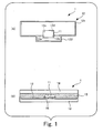
- Part (A) and part (B) of Fig. 1 are respectively a front view and a side cross section both showing an example of RFID tag.
- An RFID tag 1 shown in Fig. 1 is composed of an antenna 12 that is formed with a conductive material (such as Cu or Al or Ag paste) and disposed on a base 13 in a thin film form made of PET, polyimid and the like, an IC chip 11 with IC electrodes connected through bumps 16 to the antenna 12, a cover sheet 14 glued to the base 13 by an adhesive agent 15 such that the cover sheet 14 covers the antenna 12 and the IC chip 11.
- a conductive material such as Cu or Al or Ag paste
- the electrodes of the IC chip 11 are glued at four points of two ends 12a and 12b of the antenna 12 and two lands 12c and 12d both formed separated from the antenna on the base 13. Only the two electrodes connected to the ends 12a and 12b of the antenna 12 perform electrical effects actually, while other electrodes connected to the lands 12c and 12d are simply for fixing the IC chip stably on the base 13.
- the IC chip 11 composing the RFID tag 1 may perform radio communication with external devices with the antenna 12 to exchange information.
- the antenna 12 of the RFID tag 1 is composed of two loops 121 and 122.
- the antenna 12 is not so limited to this form.
- Other antennas with various forms such as one formed in a loop and one in a bar form extended from the both sides of the IC chip may be applied.
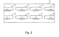
- Fig. 2 is a diagram showing a state where the antenna is formed on the base.
- a base 113 is prepared which is in a long-belt-like form extending in the right and left directions in Fig. 2 , and which is flexible and in a thin film form made of PET or polyimid, for example.
- a number of the antennas 12 for the RFID tag are formed with a predetermined pitch using a conductive material such as Ag paste.
- a respective IC chip (see Fig. 1 ) is mounted at a position indicated by circles in dotted lines in Fig. 2 .
- Fig. 3 is a process chart showing an IC chip mounting process.
- thermosetting adhesive agent 21 is applied on the IC mount position (indicated by the circles in dotted lines in Fig. 2 ) on the base 13 on which the antenna 12 is formed as shown in part (A) of Fig. 3 .
- the IC chip 11 with solder bumps 16 formed on the IC electrodes 111 is carried and placed in registration with the IC mount position on the base 13 (part (B) of Fig. 3 ). Then the IC chip 11 is pressed on the base 13 by a mounting head 31 and is simultaneously heated (part (C) of Fig. 3 ). In this manner, the IC chip 11 is glued by solder to the antenna 12 with the bump 16 and is glued on the base 13 with hardening of the adhesive agent, and then the mounting head 31 is removed (part (D) of Fig. 3 ).
- the IC chip 11 is mounted as shown above, the IC chip is covered with the cover sheet 14 as necessary. (see part (B) of Fig. 1 ).
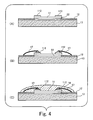
- Fig. 4 is a process chart showing another IC chip mounting process.
- thermosetting adhesive agent 22 is applied on the IC mount position (indicated by circles in dotted lines in Fig. 2 ) on the base 13 on which the antenna 12 is formed.
- the IC chip 11 is mounted at the IC mount position and glued on the base 13 by an adhesive agent 22 with the electrode 112 directed upwardly (part (A) of Fig. 4 ).
- the electrodes 112 of the IC chip 11 and the antennas 12 on the base 13 are wire-bonded with bonding wires 17(part (B) of Fig. 4 ) and then are encapsulated by a resin 18 (part (C) of Fig. 4 ).
- An assembly with IC chips mounted on respective antennas 12 as shown in Fig. 3 or Fig. 4 is called a series RFID tags.
- the series of RFID tags is rolled to be sent to manufacturing processes such as separating each of the RFID tags to be mounted on an IC card.
- Fig. 5 is a diagram showing an RFID tag roll that the series of RFID tags is reeled.
- a series RFID tags 100 that includes a number of the RFID tags formed on the base 13 having a long-belt-like form is reeled around a cylindrical core 41 to form an RFID tag roll 110.
- An arrangement similar to Fig. 5 is known from WO 01/03188 .
- the series of RFID tags 100 is reeled around the core such that the reeled series of RFID tags 100 does not show looseness
- the series of RFID tags is reeled with some tension.
- stress toward the center arises. For this reason, an excessive load is applied to an inside reeled portion of the RFID series 100.
- reeling is caused to halt for a certain period to perform an intermittent operation. In this process, because a tension is continuously applied to prevent looseness of the series of RFID tags 100 even during the time when reeling halts, reeling is performed too tightly. Hence, the load applied to an inside reeled portion is further increased.
- the present invention provides a method of reeling the RFID series to give a tension necessary and simultaneously to prevent a product defective from occurring, and an RFID tag roll into which a RFID series is formed by the method of reeling.
- a method of reeling a series of RFID tags in which a number of RFID tags each having an antenna and a circuit chip connected to the antenna and performing radio communication with the antenna are formed with a predetermined pitch on a long-belt-like and flexible base, the method including reeling the series of RFID tags around a reel core which reel core is formed by a core material characterized in that a stress absorbing material is wrapped around the core material, the stress absorbing material absorbing a stress produced during the reeling of the series of RFID tags.
- the stress absorbing material contracts and deforms in response to the stress produced during the reeling of the series of RFID tags.
- an RFID tag roll includes a series of RFID tags in which a number of RFID tags each having an antenna and a circuit chip connected to the antenna and performing radio communication with the antenna are formed with a predetermined pitch on a long-belt-like and flexible base, and a reel core around which the series of RFID tags is reeled and which is formed by a core material characterized in that a stress absorbing material is wrapped around the core material, the stress absorbing material absorbing a stress produced during reeling of the series of RFID tags.
- the stress absorbing material is provided between the core material and the series of RFID tags, the stress is absorbed by the existence of the stress absorbing material even when the series of RFID tags is reeled with a necessary tension. Therefore, defectives such as breaking of the antenna or damage of the IC chip are avoided.
- Fig. 6 is a diagram showing an RFID tag roll formed by reeling a series of RFID tags.
- the series of RFID tags 100 is reeled around a reel core 40 formed with a core material 41 and a stress absorbing material 42 wrapped around the core material 41 to form the RFID tag roll 120.
- the core material 41 shown in Fig. 6 has a diameter which is smaller than that of the core material shown in Fig. 5 by a portion for placing the stress absorbing material 42 around the core material 41.
- stress absorbing materials materials can be used such as air buffer material and sponge which are contracted and deformed by an external force.
- the RFID tag roll 120 is reeled around the reel core 40 formed by the core material 41 and the stress absorbing material 42, a load is applied to an inner reeled portion as reeling is carried out.
- the stress absorbing material 42 is thereby contracted and deformed to absorb the stress. Therefore, defectives such as breaking of the antenna and damage to the IC chip are prevented.
- the stress absorbing material 42 and the core material 41 may be adhered together and be formed integrally. Alternatively, the stress absorbing material 42 may be wrapped around the core material 41 as an independent material, before the series of RFID tags is reeled. The stress produced in an inner reeled portion depends on the length of the series of RFID tags reeled. Therefore, a stress absorbing material 42 having a thickness selected as a function of the length of the series of RFID tags to be reeled may be used.
Landscapes
- Engineering & Computer Science (AREA)
- Microelectronics & Electronic Packaging (AREA)
- Computer Hardware Design (AREA)
- Physics & Mathematics (AREA)
- General Physics & Mathematics (AREA)
- Theoretical Computer Science (AREA)
- Credit Cards Or The Like (AREA)
- Details Of Aerials (AREA)
Claims (3)
- Verfahren zum Spulen einer Serie von RFID-Etiketten (100), in der eine Anzahl von RFID-Etiketten, die jeweils eine Antenne und einen Schaltungschip haben, der mit der Antenne verbunden ist und eine Funkkommunikation mit der Antenne ausführt, mit einer vorbestimmten Teilung auf einer flexiblen Basis (13) gebildet ist, die die Form eines langen Bandes hat, welches Verfahren umfaßt:Spulen der Serie von RFID-Etiketten um einen Spulenkern (40), welcher Spulenkern aus einem Kernmaterial (41) gebildet ist, dadurch gekennzeichnet, daß ein spannungsabsorbierendes Material (42) um das Kernmaterial (41) gewickelt ist, welches spannungsabsorbierende Material (42) um das Kernmaterial (41) gewickelt ist, welches spannungsabsorbierende Material (42) eine Spannung absorbiert, die beim Spulen der Serie von RFID-Etiketten (100) erzeugt wird.
- Verfahren zum Spulen nach Anspruch 1, bei dem sich das spannungsabsorbierende Material (42) als Reaktion auf die Spannung, die beim Spulen der Serie von RFID-Etiketten erzeugt wird, kontrahiert und deformiert.
- RFID-Etikettenrolle (120) mit:einer Serie von RFID-Etiketten (100), in der eine Anzahl von RFID-Etiketten, die jeweils eine Antenne und einen Schaltungschip haben, der mit der Antenne verbunden ist und eine Funkkommunikation mit der Antenne ausführt, mit einer vorbestimmten Teilung auf einer flexiblen Basis (13) gebildet ist, die die Form eines langen Bandes hat; undeinem Spulenkern (40), um den die Serie von RFID-Etiketten gespult wird und der aus einem Kernmaterial (41) gebildet ist, dadurch gekennzeichnet, daß ein spannungsabsorbierendes Material (42) um das Kernmaterial gewickelt ist, welches spannungsabsorbierende Material eine Spannung absorbiert, die beim Spulen der Serie von RFID-Etiketten erzeugt wird.
Applications Claiming Priority (1)
| Application Number | Priority Date | Filing Date | Title |
|---|---|---|---|
| JP2006022360A JP2007206800A (ja) | 2006-01-31 | 2006-01-31 | Rfidタグシリーズの巻取方法およびrfidタグロール |
Publications (2)
| Publication Number | Publication Date |
|---|---|
| EP1814067A1 EP1814067A1 (de) | 2007-08-01 |
| EP1814067B1 true EP1814067B1 (de) | 2008-08-13 |
Family
ID=37963583
Family Applications (1)
| Application Number | Title | Priority Date | Filing Date |
|---|---|---|---|
| EP06122184A Not-in-force EP1814067B1 (de) | 2006-01-31 | 2006-10-12 | Verfahren zum Aufrollen einer RFID-Etikettserie und RFID-Etikettrolle |
Country Status (7)
| Country | Link |
|---|---|
| US (1) | US20070181726A1 (de) |
| EP (1) | EP1814067B1 (de) |
| JP (1) | JP2007206800A (de) |
| KR (1) | KR100801524B1 (de) |
| CN (1) | CN101013476A (de) |
| DE (1) | DE602006002239D1 (de) |
| TW (1) | TWI318755B (de) |
Families Citing this family (13)
| Publication number | Priority date | Publication date | Assignee | Title |
|---|---|---|---|---|
| FI124138B (fi) * | 2008-04-21 | 2014-03-31 | Smartrac Ip Bv | Menetelmä rullattavan rainan valmistamiseksi ja rullattava raina |
| MX394132B (es) | 2010-04-30 | 2025-03-24 | Spm Oil & Gas Inc | Máquinas, sistemas, métodos implementados en computadoras, y productos de programas en computadoras para probar y certificar equipo de petróleo y gas. |
| FR2963536B1 (fr) * | 2010-08-09 | 2014-02-28 | Allflex Europ | Dispositif d'identification d'un animal et dispositif de fabrication correspondant |
| USD713825S1 (en) | 2012-05-09 | 2014-09-23 | S.P.M. Flow Control, Inc. | Electronic device holder |
| AU2013266252B2 (en) | 2012-05-25 | 2017-07-06 | Spm Oil & Gas Inc. | Evaluating systems associated with wellheads |
| TWI552924B (zh) * | 2013-03-27 | 2016-10-11 | 緯創資通股份有限公司 | 電子裝置 |
| GB2544671A (en) | 2014-07-30 | 2017-05-24 | Spm Flow Control Inc | Band with RFID chip holder and identifying component |
| USD750516S1 (en) | 2014-09-26 | 2016-03-01 | S.P.M. Flow Control, Inc. | Electronic device holder |
| US11037039B2 (en) | 2015-05-21 | 2021-06-15 | S.P.M. Flow Control, Inc. | Method and system for securing a tracking device to a component |
| WO2017030870A1 (en) | 2015-08-14 | 2017-02-23 | S.P.M. Flow Control, Inc. | Carrier and band assembly for identifying and managing a component of a system associated with a wellhead |
| CN105427741A (zh) * | 2015-12-17 | 2016-03-23 | 竹林伟业科技发展(天津)股份有限公司 | 一种分区型物流标签卷 |
| SE541653C2 (en) | 2017-11-03 | 2019-11-19 | Stora Enso Oyj | Method for manufacturing an RFID tag and an RFID tag comprising an IC and an antenna |
| SE543748C2 (en) * | 2019-11-08 | 2021-07-13 | Stora Enso Oyj | Rfid label |
Family Cites Families (18)
| Publication number | Priority date | Publication date | Assignee | Title |
|---|---|---|---|---|
| US3070281A (en) * | 1960-11-02 | 1962-12-25 | Sonoco Products Co | Foam coated paper tube |
| US3522700A (en) * | 1968-10-23 | 1970-08-04 | Leesona Corp | Method and apparatus for processing yarn |
| JPH031171U (de) * | 1989-05-30 | 1991-01-08 | ||
| JPH06239533A (ja) * | 1993-02-12 | 1994-08-30 | Tenryu Ind Co Ltd | 巻取りコア |
| US6100804A (en) * | 1998-10-29 | 2000-08-08 | Intecmec Ip Corp. | Radio frequency identification system |
| AU6270599A (en) * | 1999-07-01 | 2001-01-22 | Intermec Ip Corp. | Integrated circuit attachment process and apparatus |
| US6140146A (en) * | 1999-08-03 | 2000-10-31 | Intermec Ip Corp. | Automated RFID transponder manufacturing on flexible tape substrates |
| US6478229B1 (en) * | 2000-03-14 | 2002-11-12 | Harvey Epstein | Packaging tape with radio frequency identification technology |
| JP2002134635A (ja) * | 2000-10-24 | 2002-05-10 | Toppan Forms Co Ltd | Icラベルの製造装置および製造方法 |
| US6830639B2 (en) * | 2001-05-14 | 2004-12-14 | Pittsfield Weaving Co., Inc. | Method and apparatus for producing folded labels having rounded corners |
| JP2003285978A (ja) * | 2002-03-28 | 2003-10-07 | Showa Highpolymer Co Ltd | プラスチック成形フィルム製品とその巻き取り方法及び巻き取り装置 |
| JP2004210432A (ja) * | 2002-12-27 | 2004-07-29 | Fuji Photo Film Co Ltd | 画像記録媒体ロール及びその製造方法 |
| WO2004097726A1 (ja) * | 2003-05-01 | 2004-11-11 | Brother Kogyo Kabushiki Kaisha | 無線識別ラベル、その作成方法、作成装置、無線識別ラベル用シート部材、および、無線識別ラベル作成のためのその作成装置に装着されるカートリッジ |
| JP2005352557A (ja) * | 2004-06-08 | 2005-12-22 | Oji Tac Hanbai Kk | 回路素子付き積層体、icタグの製造方法および製造装置 |
| JP4734857B2 (ja) * | 2004-06-25 | 2011-07-27 | シンフォニアテクノロジー株式会社 | Icチップ実装体の製造装置 |
| JP2006023814A (ja) * | 2004-07-06 | 2006-01-26 | Daiichi:Kk | 保護スペーサ及びその製造方法 |
| US7591863B2 (en) * | 2004-07-16 | 2009-09-22 | Semiconductor Energy Laboratory Co., Ltd. | Laminating system, IC sheet, roll of IC sheet, and method for manufacturing IC chip |
| WO2006070790A1 (ja) * | 2004-12-27 | 2006-07-06 | Brother Kogyo Kabushiki Kaisha | ラベル作成装置、マーク及びテープエンド検出装置、ラベル用テープロール及びカートリッジ、マーク付テープ |
-
2006
- 2006-01-31 JP JP2006022360A patent/JP2007206800A/ja active Pending
- 2006-10-11 TW TW095137305A patent/TWI318755B/zh not_active IP Right Cessation
- 2006-10-12 EP EP06122184A patent/EP1814067B1/de not_active Not-in-force
- 2006-10-12 DE DE602006002239T patent/DE602006002239D1/de active Active
- 2006-10-18 US US11/582,505 patent/US20070181726A1/en not_active Abandoned
- 2006-10-31 KR KR1020060106127A patent/KR100801524B1/ko not_active Expired - Fee Related
- 2006-11-07 CN CNA2006101444236A patent/CN101013476A/zh active Pending
Also Published As
| Publication number | Publication date |
|---|---|
| KR20070078965A (ko) | 2007-08-03 |
| CN101013476A (zh) | 2007-08-08 |
| US20070181726A1 (en) | 2007-08-09 |
| DE602006002239D1 (de) | 2008-09-25 |
| JP2007206800A (ja) | 2007-08-16 |
| TW200805170A (en) | 2008-01-16 |
| KR100801524B1 (ko) | 2008-02-12 |
| EP1814067A1 (de) | 2007-08-01 |
| TWI318755B (en) | 2009-12-21 |
Similar Documents
| Publication | Publication Date | Title |
|---|---|---|
| EP1814067A1 (de) | Verfahren zum Aufrollen einer RFID-Etikettserie und RFID-Etikettrolle | |
| US7619530B2 (en) | RFID tag | |
| KR100553412B1 (ko) | 트랜스폰더를 제조하기 위해 캐리어 테이프 상에 배치된안테나에 마이크로칩을 접속하는 방법 | |
| US20070164867A1 (en) | Thin ic tag and method for manufacturing same | |
| AU2011288522A1 (en) | Device for identifying an animal and corresponding manufacturing device | |
| JP2006139772A (ja) | 極超短波用のラジオ周波数認識タグ及びその認識タグの製造方法 | |
| US6762682B2 (en) | Method of manufacturing electronic tag | |
| KR20140123562A (ko) | Rfid 안테나 모듈 및 방법 | |
| WO2018155382A1 (ja) | Rfidタグ | |
| US20080129455A1 (en) | Method for forming rfid tags | |
| EP1873694A1 (de) | Produktionsverfahren für ein RFID Etikett und RFID Etikett | |
| JP4386023B2 (ja) | Ic実装モジュールの製造方法および製造装置 | |
| JP4171255B2 (ja) | 電子タグの製造方法 | |
| MX2012010283A (es) | Un dispositivo de chip electronico y un proceso de fabricacion por embobinado. | |
| EP1713025A1 (de) | Teilesatz für ein RFID Tag, RFID Tag und Teil eines RFID Tags | |
| JP5886174B2 (ja) | 非接触通信媒体の製造方法、非接触通信媒体、及びアンテナと回路装置の接続方法 | |
| WO2007011954A2 (en) | Rfid tags for pallets and cartons and system for attaching same | |
| JPH1134557A (ja) | Icモジュールの製造方法、およびその製造方法に用いられるicモジュール集合体の製造装置 | |
| CN109074507B (zh) | 载带及其制造方法、以及rfid标签的制造方法 | |
| KR100467634B1 (ko) | 스마트 카드 및 그의 제조방법 | |
| KR101098289B1 (ko) | Rfid 태그, 이의 제작방법, 이를 이용한 패키징 구조체 및 제작방법 | |
| US7704790B2 (en) | Method of manufacturing a carrier member for electronic components | |
| JP4736557B2 (ja) | Icカード用icモジュールとその製造方法 | |
| JP2015228234A (ja) | 非接触通信媒体の製造方法、及びアンテナと回路装置の接続方法 | |
| US12635120B2 (en) | Wireless communication device manufacturing method and wireless communication device manufacturing apparatus |
Legal Events
| Date | Code | Title | Description |
|---|---|---|---|
| PUAI | Public reference made under article 153(3) epc to a published international application that has entered the european phase |
Free format text: ORIGINAL CODE: 0009012 |
|
| AK | Designated contracting states |
Kind code of ref document: A1 Designated state(s): AT BE BG CH CY CZ DE DK EE ES FI FR GB GR HU IE IS IT LI LT LU LV MC NL PL PT RO SE SI SK TR |
|
| AX | Request for extension of the european patent |
Extension state: AL BA HR MK YU |
|
| 17P | Request for examination filed |
Effective date: 20070712 |
|
| GRAP | Despatch of communication of intention to grant a patent |
Free format text: ORIGINAL CODE: EPIDOSNIGR1 |
|
| GRAS | Grant fee paid |
Free format text: ORIGINAL CODE: EPIDOSNIGR3 |
|
| AKX | Designation fees paid |
Designated state(s): DE FR GB |
|
| GRAA | (expected) grant |
Free format text: ORIGINAL CODE: 0009210 |
|
| AK | Designated contracting states |
Kind code of ref document: B1 Designated state(s): DE FR GB |
|
| REG | Reference to a national code |
Ref country code: GB Ref legal event code: FG4D |
|
| REF | Corresponds to: |
Ref document number: 602006002239 Country of ref document: DE Date of ref document: 20080925 Kind code of ref document: P |
|
| PLBE | No opposition filed within time limit |
Free format text: ORIGINAL CODE: 0009261 |
|
| STAA | Information on the status of an ep patent application or granted ep patent |
Free format text: STATUS: NO OPPOSITION FILED WITHIN TIME LIMIT |
|
| 26N | No opposition filed |
Effective date: 20090514 |
|
| PGFP | Annual fee paid to national office [announced via postgrant information from national office to epo] |
Ref country code: DE Payment date: 20101006 Year of fee payment: 5 |
|
| PGFP | Annual fee paid to national office [announced via postgrant information from national office to epo] |
Ref country code: GB Payment date: 20101026 Year of fee payment: 5 |
|
| PGFP | Annual fee paid to national office [announced via postgrant information from national office to epo] |
Ref country code: FR Payment date: 20111103 Year of fee payment: 6 |
|
| GBPC | Gb: european patent ceased through non-payment of renewal fee |
Effective date: 20121012 |
|
| REG | Reference to a national code |
Ref country code: FR Ref legal event code: ST Effective date: 20130628 |
|
| PG25 | Lapsed in a contracting state [announced via postgrant information from national office to epo] |
Ref country code: DE Free format text: LAPSE BECAUSE OF NON-PAYMENT OF DUE FEES Effective date: 20130501 Ref country code: GB Free format text: LAPSE BECAUSE OF NON-PAYMENT OF DUE FEES Effective date: 20121012 |
|
| REG | Reference to a national code |
Ref country code: DE Ref legal event code: R119 Ref document number: 602006002239 Country of ref document: DE Effective date: 20130501 |
|
| PG25 | Lapsed in a contracting state [announced via postgrant information from national office to epo] |
Ref country code: FR Free format text: LAPSE BECAUSE OF NON-PAYMENT OF DUE FEES Effective date: 20121031 |