EP1814164A2 - Dispositif électroluminescent à semi-conducteur de nitrure - Google Patents
Dispositif électroluminescent à semi-conducteur de nitrure Download PDFInfo
- Publication number
- EP1814164A2 EP1814164A2 EP07001335A EP07001335A EP1814164A2 EP 1814164 A2 EP1814164 A2 EP 1814164A2 EP 07001335 A EP07001335 A EP 07001335A EP 07001335 A EP07001335 A EP 07001335A EP 1814164 A2 EP1814164 A2 EP 1814164A2
- Authority
- EP
- European Patent Office
- Prior art keywords
- layer
- quantum well
- generating device
- composition
- light generating
- Prior art date
- Legal status (The legal status is an assumption and is not a legal conclusion. Google has not performed a legal analysis and makes no representation as to the accuracy of the status listed.)
- Withdrawn
Links
Images





Classifications
-
- H—ELECTRICITY
- H10—SEMICONDUCTOR DEVICES; ELECTRIC SOLID-STATE DEVICES NOT OTHERWISE PROVIDED FOR
- H10H—INORGANIC LIGHT-EMITTING SEMICONDUCTOR DEVICES HAVING POTENTIAL BARRIERS
- H10H20/00—Individual inorganic light-emitting semiconductor devices having potential barriers, e.g. light-emitting diodes [LED]
- H10H20/80—Constructional details
- H10H20/81—Bodies
- H10H20/822—Materials of the light-emitting regions
- H10H20/824—Materials of the light-emitting regions comprising only Group III-V materials, e.g. GaP
- H10H20/825—Materials of the light-emitting regions comprising only Group III-V materials, e.g. GaP containing nitrogen, e.g. GaN
-
- B—PERFORMING OPERATIONS; TRANSPORTING
- B82—NANOTECHNOLOGY
- B82Y—SPECIFIC USES OR APPLICATIONS OF NANOSTRUCTURES; MEASUREMENT OR ANALYSIS OF NANOSTRUCTURES; MANUFACTURE OR TREATMENT OF NANOSTRUCTURES
- B82Y20/00—Nanooptics, e.g. quantum optics or photonic crystals
-
- H—ELECTRICITY
- H10—SEMICONDUCTOR DEVICES; ELECTRIC SOLID-STATE DEVICES NOT OTHERWISE PROVIDED FOR
- H10H—INORGANIC LIGHT-EMITTING SEMICONDUCTOR DEVICES HAVING POTENTIAL BARRIERS
- H10H20/00—Individual inorganic light-emitting semiconductor devices having potential barriers, e.g. light-emitting diodes [LED]
- H10H20/80—Constructional details
- H10H20/81—Bodies
- H10H20/811—Bodies having quantum effect structures or superlattices, e.g. tunnel junctions
- H10H20/812—Bodies having quantum effect structures or superlattices, e.g. tunnel junctions within the light-emitting regions, e.g. having quantum confinement structures
-
- H—ELECTRICITY
- H10—SEMICONDUCTOR DEVICES; ELECTRIC SOLID-STATE DEVICES NOT OTHERWISE PROVIDED FOR
- H10H—INORGANIC LIGHT-EMITTING SEMICONDUCTOR DEVICES HAVING POTENTIAL BARRIERS
- H10H20/00—Individual inorganic light-emitting semiconductor devices having potential barriers, e.g. light-emitting diodes [LED]
- H10H20/80—Constructional details
- H10H20/81—Bodies
-
- H—ELECTRICITY
- H10—SEMICONDUCTOR DEVICES; ELECTRIC SOLID-STATE DEVICES NOT OTHERWISE PROVIDED FOR
- H10H—INORGANIC LIGHT-EMITTING SEMICONDUCTOR DEVICES HAVING POTENTIAL BARRIERS
- H10H20/00—Individual inorganic light-emitting semiconductor devices having potential barriers, e.g. light-emitting diodes [LED]
- H10H20/80—Constructional details
- H10H20/81—Bodies
- H10H20/816—Bodies having carrier transport control structures, e.g. highly-doped semiconductor layers or current-blocking structures
Definitions
- the present invention relates to a nitride semiconductor light generating device.
- Patent Publication 1 discloses a nitride semiconductor light generating device having an active region of a double heterostructure.
- the nitride semiconductor light generating device includes an active layer having the oxygen atom concentration of Qa (atoms/cm 3 ) and made of n-type InGaN of a multiple layer structure having primary and secondary layers the indium content of which are different from each other.
- the active layer is sandwiched by an n-type cladding layer of group III nitride semiconductor of an oxygen atom concentration Qc (atoms/cm 3 ) which is smaller than or equal to Qa, and a p-type cladding layer of group III nitride semiconductor of an oxygen atom concentration Qp (atoms/cm 3 ) which is greater than or equal to Qc and smaller than or equal to Qa.
- Patent Publication 1 In the nitride light generating device of Patent Publication 1, the active layer of the oxygen atom concentration Qa is sandwiched by the n-type cladding layer of the oxygen atom concentration Qc and the p-type cladding layer of the oxygen atom concentration Qp. Patent Publication 1 does not provide any teaching of the active layer including an InAlGaN semiconductor layer.
- a nitride semiconductor light generating device comprises: (a) an n-type gallium nitride based semiconductor layer; (b) a quantum well active layer including an In X1 Al Y1 Ga 1-X1-Y1 N (1>X1>0, 1>Y1>0) well layer and an In X2 Al Y2 Ga 1-X2-Y2 N (1>X2>0, 1>Y2>0) barrier layer; (c) an In X3 Al Y3 Ga 1-X3-Y3 N (1>X3>0, 1>Y3>0) layer provided between the quantum well active layer and the n-type gallium nitride based semiconductor layer, an indium composition X3 of the In X3 Al Y3 Ga 1-X3 - Y3 N layer being greater than an indium composition X1 of the In X1 Al Y1 Ga 1-X1-Y1 N well layer, an indium composition X3 of the In X3 Al Y
- the In X3 Al Y3 Ga 1-X3-Y3 N layer has an excellent buffering ability because the indium composition X3 of the In X3 Al Y3 Ga 1-X3-Y3 N layer is greater than the indium composition X1 of the In X1 Al Y1 Ga 1-X1-Y1 N well layer and is greater than the indium composition X2 of the In X2 Al Y2 Ga 1-X2-Y2 N barrier layer. Therefore, the light generating quantum well layer has an excellent crystalline quality.
- the indium composition X1 of the In X1 Al Y1 Ga 1-X1-Y1 N well layer is smaller than the indium composition X3 of the In X3 Al Y3 Ga 1-X3-Y3 N layer and the indium composition X2 of the In X2 Al Y2 Ga 1-X2-Y2 N barrier layer is smaller than the indium composition X3 of the In X3 Al Y3 Ga 1-X3-Y3 N layer
- the aluminum composition Y1 of the In X1 Al Y1 Ga 1-X1-Y1 N well layer 13a is decreased as compared to the aluminum composition Y3 of the In X3 Al Y3 Ga 1-X3-Y3 N layer.
- the aluminum composition Y2 of the In X2 Al Y2 Ga 1-X2-Y2 N barrier layer is decreased as compared to the aluminum composition Y3 of the In X3 Al Y3 Ga 1-X3-Y3 N layer to obtain the In X1 Al Y1 Ga 1-X1-Y1 N well layer and In X2 Al Y2 Ga 1-X2-Y2 N well layer each having the desired value of bandgap energy.
- the oxygen concentration of the quantum well active layer is lowered as compared to the oxygen concentration of the In X3 Al Y3 Ga 1-X3-Y3 N layer.
- an oxygen concentration of the In X3 Al Y3 Ga 1-X3-Y3 N layer be greater than or equal to 1 ⁇ 10 18 cm -3 .
- an oxygen concentration of the In X3 Al Y3 Ga 1-X3-Y3 N layer be greater than or equal to 1 ⁇ 10 18 cm -3 .
- an oxygen concentration of the In X3 Al Y3 Ga 1-X3-Y3 N layer be lower than or equal to 1 ⁇ 10 20 cm -3 . If this oxygen concentration is increased above 1 ⁇ 10 20 cm -3 , the crystalline quality of the In X3 Al Y3 Ga 1-X3-Y3 N layer is lowered and this lowering affects the crystalline quality of the quantum well active layer.
- an oxygen concentration of the quantum well active layer be lower than 1 ⁇ 10 18 cm -3 . If the well layer has an oxygen concentration greater than or equal to 1 ⁇ 10 18 cm -3 , this affects its crystalline quality and the electron leakage to the p-type AlGaN layer is increased.
- an oxygen concentration of the quantum well active layer be greater than or equal to 1 ⁇ 10 16 cm -3 .
- the growth temperature has to be raised to obtain the oxygen concentration lower than 1 ⁇ 10 16 cm -3 , and the indium concentration of the quantum well active layer is lowered thereby deteriorating the light generation efficiency.
- the nitride semiconductor light generating device further comprises a group III nitride substrate, and the n-type gallium nitride based semiconductor layer is provided between the In X3 Al Y3 Ga 1-X3-Y3 N layer and the group III nitride substrate.
- group III nitride substrate 21 gallium nitride based semiconductor having an excellent crystalline quality can be grown thereon.
- the group III nitride substrate include a gallium nitride substrate.
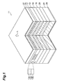
- Fig. 1 is a schematic view showing the structure of a nitride light generating device according to a first embodiment of the present invention
- Fig. 2 is a view showing fabrication steps for structures 1 and 2
- Fig. 3 is a view showing fabrication steps for structure 1
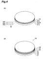
- Fig. 4 is a view showing fabrication steps for structure 2
- Fig. 5 is a schematic view showing a light emitting diode of the structure 1
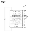
- Fig. 6 is a schematic view showing a light emitting diode of the structure 2
- Fig. 7 is a view showing the optical spectrums of the structure 1 measured at the temperatures of 300 K and 210K
- Fig. 8 is a view showing the optical spectrums of the structure 2 measured at the temperatures of 300 K and 210K
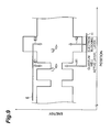
- Fig. 9 is a view showing a band diagram of the structure 1.
- Fig. 1 is a view showing the structure of a nitride semiconductor light generating device.
- the nitride semiconductor light generating device 11 comprises a quantum well active layer 13, an n-type gallium nitride based semiconductor 15, and a p-type AlGaN semiconductor layer 17.
- the quantum well active layer 13 includes an In X1 Al Y1 Ga 1-X1 - Y1 N (1>X1>0, 1>Y1>0) well layer 13a and an In X2 Al Y2 Ga 1-X2-Y2 N (1>X2>0, 1>Y2>0) barrier layer 13b.
- the nitride semiconductor light generating device 11 includes an InX 3 Al Y3 Ga 1-X3-Y3 N (1>X3>0, 1>Y3>0) layer 19.
- the In X3 Al Y3 Ga 1-X3-Y3 N (1>X3>0, 1>Y3>0) layer 19 is provided between the quantum well active layer 13 and the n-type gallium nitride based semiconductor layer 15.
- the p-type AlGaN layer 17 has the bandgap energy E CP greater than the bandgap energy E B of the In X2 Al Y2 Ga 1-X2-Y2 N barrier layer.13b.
- the quantum well active layer 13 is provided between the p-type AlGaN layer 17 and the In X3 Al Y3 Ga 1-X3-Y3 N layer 19.
- the indium composition X3 of the In X3 Al Y3 Ga 1-X3-Y3 N layer 19 is greater than the indium composition X1 of the In X1 Al Y1 Ga 1-X1-Y1 N well layer 13a.
- the indium composition X3 of the In X3 Al Y3 Ga 1-X3-Y3 N layer 19 is greater than the indium composition X2 of the In X2 Al Y2 Ga 1-X2-Y2 N barrier layer 13b.
- the aluminum composition Y1 of the In X1 Al Y1 Ga 1-X1-Y1 N well layer 13a is smaller than the aluminum composition Y3 of the In X3 Al Y3 Ga 1-X3-Y3 N layer 19.
- the aluminum composition Y2 of the In X2 Al Y2 Ga 1-X2-Y2 N barrier layer 13b is smaller than the aluminum composition Y3 of the In X3 Al Y3 Ga 1-X3-Y3 N layer 19.
- the oxygen concentration of the quantum well active layer 13 is lower than that of the In X3 Al Y3 Ga 1-X3-Y3 N layer 19.
- the In X3 Al Y3 Ga 1-X3-Y3 N layer 19 has an excellent buffering ability because the indium composition X3 of the In X3 Al Y3 Ga 1-X3-Y3 N layer 19 is greater than the indium composition X1 of the In X1 Al Y1 Ga 1-X1-Y1 N well layer 13a and the indium composition X3 of the In X3 Al Y3 Ga 1-X3-Y3 N layer 19 is greater than the indium composition X2 of the In X2 Al Y2 Ga 1-X2-Y2 N barrier layer 13b. Therefore, the optical performances and crystalline quality of the light generating quantum well layer 13 are improved.
- the indium composition X1 of the In X1 Al Y1 Ga 1-X1-Y1 N well layer 13a is smaller than the indium composition X3 of the In X3 Al Y3 Ga 1-X3-Y3 N layer 19 and the indium composition X2 of the In X2 Al Y2 Ga 1-X2-Y2 N barrier layer 13b is smaller than the indium composition X3 of the In X3 Al Y3 Ga 1-X3-Y3 N layer 19, the aluminum composition Y1 of the In X1 Al Y1 Ga 1-X1-Y1 N well layer 13a is decreased as compared to the aluminum composition Y3 of the In X3 Al Y3 Ga 1-X3-Y3 N layer 19, and the aluminum composition Y2 of the In X2 Al Y2 Ga 1-X2-Y2 N barrier layer 13b is decreased as compared to the aluminum composition Y3 of the In X3 Al Y3 Ga 1-X3-Y3 N layer 19, thereby providing the In X1 Al Y1 Ga 1-X1
- the aluminum composition Y1 of the In X1 Al Y1 Ga 1-X1-Y1 N well layer 13a and the aluminum composition Y2 of the In X2 Al Y2 Ga 1-X2-Y2 N barrier layer 13b are smaller than the aluminum composition Y3 of the In X3 Al Y3 Ga 1-X3-Y3 N layer 19, the oxygen concentration N 13 of the quantum well active layer 13 is lower than the oxygen concentration N 19 of the In X3 Al Y3 Ga 1-X3-Y3 N layer 19. Since the concentration of oxygen acting as n-type dopant is decreased in the quantum well active layer 13, electron leakage to the p-type AlGaN layer is reduced thereby enhancing the light emitting efficiency.
- the quantum well active layer 13 is provided to generate light in an ultraviolet wavelength region.
- the peak wavelength of the light is in the range of 260 nanometers to 360 nanometers. Since the quantum well active layer 13 has a quantum well structure, this quantum well structure is constituted to generate light of a desired wavelength in the ultraviolet wavelength region by adjusting bandgap energy widths and/or compositions of the well layer and barrier layer.
- the nitride semiconductor light generating device 11 further comprises a group III nitride substrate 21.
- the n-type gallium nitride based semiconductor 15 is provided between the In X3 Al Y3 Ga 1-X3-Y3 N layer 19 and the group III nitride substrate 21.
- group III nitride substrate 21 gallium nitride based semiconductor having an excellent crystalline quality is grown thereon.
- the group III nitride substrate 21 is an n-type gallium nitride substrate. Accordingly, the nitride semiconductor light generating device 11 is provided with a substrate having a low threading dislocation density.
- the nitride semiconductor light generating device 11 further comprises a buffer layer 23 provided on the group III nitride substrate 21.
- the buffer layer 23 is made of n-type gallium nitride based semiconductor.
- This n-type gallium nitride based semiconductor is, for example, n-type GaN or n-type AlGaN.
- the nitride semiconductor light generating device 11 further comprises a p-type gallium nitride based semiconductor layer 25 provided the p-type AlGaN layer 17.
- the p-type gallium nitride based semiconductor layer 25 has a bandgap energy smaller than that of the p-type AlGaN layer 17, and is made of, for example, p-type GaN or p-type AlGaN.
- the nitride semiconductor light generating device 11 further comprises a first electrode 27 provided the p-type gallium nitride based semiconductor layer 25, and a second electrode 29 provided on the back side of the group III nitride substrate 21.
- the first electrode 27 works as an anode electrode and the second electrode works as a cathode electrode.
- the oxygen concentration N 19 of the In X3 Al Y3 Ga 1-X3-Y3 N layer 19 be greater than or equal to 1 ⁇ 10 18 cm -3 .
- the oxygen concentration N 19 of the In X3 Al Y3 Ga 1-X3-Y3 N layer 19 be greater than or equal to 1 ⁇ 10 18 cm -3 .
- the oxygen concentration N 19 of the In X3 Al Y3 Ga 1-X3-Y3 N layer 19 be smaller than or equal to 1 ⁇ 10 20 cm -3 . If the oxygen concentration is greater than 1 ⁇ 10 20 cm -3 , the crystalline quality of the In X3 Al Y3 Ga 1-X3-Y3 N layer is deteriorated and this lowering affects the crystalline quality of the quantum well active layer 13.
- the oxygen concentration N 13 of the quantum well active layer 13 be smaller than 1 ⁇ 10 18 cm -3 . If the oxygen concentration of the quantum well active layer 13 is greater than or equal to 1 ⁇ 10 18 cm -3 , this affects the crystalline quality of the quantum well active layer 13 and also causes the increase of the electron leakage to the p-type AlGaN layer.
- the oxygen concentration N 13 of the quantum well active layer 13 be greater than or equal to 1 ⁇ 10 16 cm- 3 . If the oxygen concentration of the quantum well active layer 13 is lower than 1 ⁇ 10 16 cm -3 , the indium concentration is decreased and light generation efficiency is deteriorated.
- the oxygen concentration of the well layer 13a be lower than 1 ⁇ 10 18 cm -3 . If the well layer 13a has an oxygen concentration greater than or equal to 1 ⁇ 10 18 cm -3 , this affects the crystalline quality of the quantum well layer 13a and also causes the increase of the electron leakage to the p-type AlGaN layer.
- the oxygen concentration of the well layer 13a be greater than or equal to 1 ⁇ 10 16 cm -3 .
- the growth temperature has to be raised so that the oxygen concentration decreased below 1 ⁇ 10 16 cm -3 , and the indium concentration is lowered, thereby decreasing the light generation efficiency.
- the oxygen concentration of the barrier layer 13b be lower than 1 ⁇ 10 18 cm -3 . If the barrier layer 13b has an oxygen concentration greater than or equal to 1 ⁇ 10 18 cm -3 , this affects the crystalline quality of the barrier layer 13b and also causes the increase of the electron leakage to the p-type AlGaN layer.
- the oxygen concentration of the barrier layer 13b be greater than or equal to 1 ⁇ 10 16 cm -3 .
- the growth temperature has to be raised so that the oxygen concentration is decreased lower than 1 ⁇ 10 16 cm -3 , and the indium concentration of the barrier layer 13b is lowered, thereby decreasing the light generation efficiency.
- a gallium nitride wafer 31 is prepared.
- the gallium nitride wafer 31 has an electrical conductivity and is made of n-type GaN.
- the gallium nitride wafer 31 is set in an organo-metallic vapor phase epitaxy furnace, and a thermal cleaning of the gallium nitride wafer 31 is performed.
- the temperature of the organo-metallic vapor phase epitaxy furnace is set at the temperature of 1050 degrees Celsius.
- Gas containing ammonia and hydrogen (NH 3 + H 2 ) is supplied to the organo-metallic vapor phase epitaxy furnace to perform the thermal cleaning for ten minutes, for example.
- an n-type GaN film 33 is grown on the GaN wafer 31 using the organo-metallic vapor phase epitaxy furnace. This growth is performed at the temperature of 1150 degrees Celsius, for example, and the thickness of the n-type GaN film 33 is two micrometers, for example. Then, an n-type AlGaN film 35 is grown on the n-type GaN film 33. This growth is performed at the temperature of, for example, 1080 degrees Celsius.
- the composition of the n-type AlGaN film 35 is, for example, Al 0.18 Ga 0.82 N, and the thickness of the n-type AlGaN film 35 is, for example, 30 nanometers.
- an n-type InAlGaN buffer layer 37 (hereinafter referred to as the In X3 Al Y3 Ga 1-X3-Y3 N (1 > X3 >0, 1 > Y3 >0) as with the first embodiment) is grown on the n-type AlGaN film 35.
- the growth is performed at the temperature of 780 degrees Celsius, for example.
- the composition of the n-type InAlGaN buffer layer 37 is, for example, In 0.05 Al 0.24 Ga 0.71 N, and its thickness is, for example, 35 nanometers.
- a quantum well active region 39 for structure 1 is grown on the epitaxial wafer "B."
- the quantum well active region 39 includes a well layer 39a and a barrier layer 39b.
- the well layer 39a is an In U1 Al V1 Ga 1-U1-V1 N (1 > U1 >0, 1 > V1 >0).
- the barrier layer 39b is an In U2 Al V2 Ga 1-U2-V2 N (1 > U2 >0, 1 > V2 >0).
- the formation temperature of the quantum well active region 39 is substantially the same as the growth temperature of the InAlGaN buffering layer 37.
- the growth of the quantum well active region 39 is performed at the temperature of 780 degrees Celsius.
- the composition of the well layer 39a is In 0.06 Al 0.19 Ga 0.75 N and the composition of the barrier layer 39b is In 0.05 Al 0.24 Ga 0.71 N.
- the thickness of the In 0.06 Al 0.19 Ga 0.75 N well layer is 2.5 nanometers and the thickness of the In 0.05 Al 0.24 Ga 0.71 N barrier layer is 15 nanometers.
- a p-type AlGaN film 41 for blocking electrons is formed using the organo-metallic vapor phase epitaxy furnace. This growth is performed at the temperature of 1030 degrees Celsius, for example.
- the composition of the p-type AlGaN film 41 is, for example, Al 0.27 Ga 0.73 N and the thickness of the p-type AlGaN film 41 is, for example, 25 nanometers.
- a p-type AlGaN film 43 for forming an excellent ohmic contact is grown using the organo-metallic vapor phase epitaxy furnace. This growth is performed at the temperature of 1030 degrees Celsius.
- the composition of the p-type AlGaN film 43 is, for example, Al 0.18 Ga 0.82 N and the thickness of the p-type AlGaN film 43 is, for example, 60 nanometers. These steps provide an epitaxial wafer "B1."
- a quantum well active region 45 for structure 2 is grown on the epitaxial wafer "B."
- the quantum well active region 45 includes a well layer 45a and a barrier layer 45b.
- the well layer 45a is an In X1 Al Y1 Ga 1-X1-Y1 N (1 > X1 >0, 1 > Y1 >0).
- the barrier layer 45b is an In X2 Al Y2 Ga 1-X2-Y2 N (1 > X2 >0, 1 > Y2 >0).
- the formation temperature of the quantum well active region 45 is higher than the growth temperature of the InAlGaN buffering layer 37. In the present embodiment, the growth of the quantum well active region 45 is performed at the temperature of 830 degrees Celsius.
- the indium composition X3 of the In X3 Al Y3 Ga 1-X3 - Y3 N layer is greater than the indium composition X1 of the In X1 Al Y1 Ga 1-X1-Y1 N well layer, and the indium composition X3 of the In X3 Al Y3 Ga 1-X3 - Y3 N layer is greater than the indium composition X2 of the In X2 Al Y2 Ga 1 - X2-Y2 N barrier layer.
- the aluminum composition Y1 of the Inx 1 Al Y1 Ga 1-X1-Y1 N well layer is smaller than the aluminum composition Y3 of the In X3 Al Y3 Ga 1-X3-Y3 N layer
- the aluminum composition Y2 of the In X2 Al Y2 Ga 1-X2-Y2 N barrier layer is smaller than the aluminum composition Y3 of the In X3 Al Y3 Ga 1-X3-Y3 N layer.
- the composition of the well layer 45a is In 0.02 Al 0.09 Ga 0.81 N and the composition of the barrier layer 45b is In 0.02 Al 0.22 Ge 0.76 N.
- the thickness of the In 0.02 Al 0.09 Ga 0.81 N well layer is 2.7 nanometers and the thickness of the In 0.02 Al 0.22 Ga 0.76 N barrier layer is 15 nanometers.
- a p-type AlGaN film 47 is formed using the organo-metallic vapor phase epitaxy furnace. This growth is performed at the temperature of 1030 degrees Celsius, for example.
- the composition of the p-type AlGaN film 47 is, for example, Al 0.27 Ga 0.73 N and the thickness of the p-type AlGaN film 47 for blocking electrons is, for example, 25 nanometers.
- a p-type AlGaN film 49 for forming an excellent ohmic contact is grown using the organo-metallic vapor phase epitaxy furnace. This growth is performed at the temperature of 1030 degrees Celsius.
- composition of the p-type AlGaN film 49 is, for example, Al 1.18 Ga 0.82 N and the thickness of the p-type AIGaN film 49 is, for example, 60 nanometers. These steps provide an epitaxial wafer "B2.”
- the epitaxial substrates "B1" and “B2” are analyzed by SIMS method to estimate the oxygen concentrations of the quantum well active layers 39, 45.
- the oxygen concentrations of the quantum well active layer 39 and buffering layer in the epitaxial substrate “B1” both are about 1 ⁇ 10 18 cm -3 .
- the oxygen concentrations of the quantum well active layer 45 and buffering layer in the epitaxial substrate “B2” are about 5 ⁇ 10 17 cm -3 and about 1 ⁇ 10 18 cm -3 , respectively. This shows that the oxygen concentration is reduced by increase the growth temperature of AlInGaN. The reduction of oxygen concentrations provides the excellent crystal quality.
- An anode electrode 51 a such as Ni/Au
- a cathode electrode 51b such as Ti/Al
- An anode electrode 53a such as Ni/Au
- a cathode electrode 53b such as Ti/A1
- the above board signal in the emission spectrum of the LED structure "S1" comes from emission by the p-type AlGaN region.
- the efficiency of this emission is not strong at room temperature. But, as the temperature is lowered, this emission efficiency becomes high and the electrical characteristics of the p-type AlGaN region are deteriorated, thereby causing the leakage of electron from the quantum well active region.
- the emission from the leakage of electron appears in the emission spectrum of the LED structure "S 1."
- the emission spectrum of the LED structure "S2" does not have any board signal as above. That is, as shown in Fig.
- the leakage "E1" of electron is increased in the quantum well active layer having a high oxygen concentration, and this deteriorates the injection efficiency because oxygen acts as donor in the gallium nitride based semiconductor.
- the recombination of electrons "E1" and holes “H1" in the quantum well active layer generates light having a wavelength component of 350 nanometers (ultraviolet light).
- the recombination of electrons E2 and holes H2 in the quantum well active layer generates light having a wavelength component of 390 nanometers.
- This emission relates to deep acceptor level form magnesium (Mg) and appears as a board signal in the emission spectrum around 390 nanometers.
- the peak intensity of the LED structure "S2" is twice as high as that of the LED structure "S1.” This comes from the following:
Landscapes
- Chemical & Material Sciences (AREA)
- Engineering & Computer Science (AREA)
- Nanotechnology (AREA)
- Physics & Mathematics (AREA)
- Life Sciences & Earth Sciences (AREA)
- Biophysics (AREA)
- Optics & Photonics (AREA)
- Crystallography & Structural Chemistry (AREA)
- Led Devices (AREA)
- Semiconductor Lasers (AREA)
Applications Claiming Priority (1)
| Application Number | Priority Date | Filing Date | Title |
|---|---|---|---|
| JP2006018159A JP2007201195A (ja) | 2006-01-26 | 2006-01-26 | 窒化物半導体発光素子 |
Publications (2)
| Publication Number | Publication Date |
|---|---|
| EP1814164A2 true EP1814164A2 (fr) | 2007-08-01 |
| EP1814164A3 EP1814164A3 (fr) | 2008-11-05 |
Family
ID=37897738
Family Applications (1)
| Application Number | Title | Priority Date | Filing Date |
|---|---|---|---|
| EP07001335A Withdrawn EP1814164A3 (fr) | 2006-01-26 | 2007-01-22 | Dispositif électroluminescent à semi-conducteur de nitrure |
Country Status (6)
| Country | Link |
|---|---|
| US (1) | US7576351B2 (fr) |
| EP (1) | EP1814164A3 (fr) |
| JP (1) | JP2007201195A (fr) |
| KR (1) | KR20070078382A (fr) |
| CN (1) | CN100573942C (fr) |
| TW (1) | TW200742129A (fr) |
Cited By (3)
| Publication number | Priority date | Publication date | Assignee | Title |
|---|---|---|---|---|
| WO2011080144A3 (fr) * | 2009-12-30 | 2011-12-22 | Osram Opto Semiconductors Gmbh | Puce semiconductrice optoélectronique et utilisation d'une couche intermédiaire à base de algan |
| EP2472606A4 (fr) * | 2009-07-15 | 2015-01-07 | Sumitomo Electric Industries | Élément optique semiconducteur en nitrure de groupe iii |
| EP2352182A4 (fr) * | 2008-10-20 | 2015-02-11 | Sumitomo Electric Industries | Procede de fabrication d' un element emetteur de lumiere semi-conducteur au nitrure et procede de fabrication d' une plaquette epitaxique |
Families Citing this family (15)
| Publication number | Priority date | Publication date | Assignee | Title |
|---|---|---|---|---|
| SG115549A1 (en) * | 2002-07-08 | 2005-10-28 | Sumitomo Chemical Co | Epitaxial substrate for compound semiconductor light emitting device, method for producing the same and light emitting device |
| CN102569557A (zh) * | 2007-07-17 | 2012-07-11 | 住友电气工业株式会社 | 电子器件的制作方法、外延衬底的制作方法、iii族氮化物半导体元件及氮化镓外延衬底 |
| KR101018088B1 (ko) * | 2008-11-07 | 2011-02-25 | 삼성엘이디 주식회사 | 질화물 반도체 소자 |
| JP2010212651A (ja) * | 2009-09-08 | 2010-09-24 | Sumitomo Electric Ind Ltd | Iii族窒化物半導体素子、エピタキシャル基板、及びiii族窒化物半導体素子を作製する方法 |
| KR101007087B1 (ko) | 2009-10-26 | 2011-01-10 | 엘지이노텍 주식회사 | 발광소자 및 그 제조방법 |
| DE102009060747B4 (de) * | 2009-12-30 | 2025-01-09 | OSRAM Opto Semiconductors Gesellschaft mit beschränkter Haftung | Halbleiterchip |
| CN102280547A (zh) * | 2011-08-31 | 2011-12-14 | 厦门大学 | 一种有源区为p型的氮化镓系半导体发光管 |
| CN102368519B (zh) * | 2011-10-27 | 2016-04-20 | 华灿光电股份有限公司 | 一种提高半导体二极管多量子阱发光效率的方法 |
| CN102623596A (zh) * | 2012-04-25 | 2012-08-01 | 华灿光电股份有限公司 | 一种具有倾斜量子阱结构的氮化镓半导体发光二极管 |
| EP2973664B1 (fr) * | 2013-03-15 | 2020-10-14 | Crystal Is, Inc. | Dispositif émetteur d'ultraviolet et procédé pour former un contact sur un dispositif émetteur d'ultraviolet |
| KR102181482B1 (ko) * | 2014-06-16 | 2020-11-23 | 엘지이노텍 주식회사 | 발광소자 및 조명시스템 |
| JP6721816B2 (ja) * | 2015-06-29 | 2020-07-15 | 株式会社タムラ製作所 | 窒化物半導体テンプレート及び紫外線led |
| JP6654596B2 (ja) | 2017-03-24 | 2020-02-26 | 日機装株式会社 | 半導体発光素子および半導体発光素子の製造方法 |
| US10156335B1 (en) * | 2017-08-01 | 2018-12-18 | Epistar Corporation | Light-emitting device |
| CN117691019B (zh) * | 2024-02-02 | 2024-04-30 | 江西兆驰半导体有限公司 | 一种P型GaN层发光二极管外延片及制备方法 |
Family Cites Families (9)
| Publication number | Priority date | Publication date | Assignee | Title |
|---|---|---|---|---|
| JPH06164055A (ja) * | 1992-11-25 | 1994-06-10 | Asahi Chem Ind Co Ltd | 量子井戸型半導体レーザ |
| JP2956623B2 (ja) * | 1996-12-02 | 1999-10-04 | 日本電気株式会社 | 自励発振型半導体レーザ素子 |
| JP3371828B2 (ja) | 1998-11-24 | 2003-01-27 | 昭和電工株式会社 | 窒化物半導体発光素子 |
| US6570898B2 (en) * | 1999-09-29 | 2003-05-27 | Xerox Corporation | Structure and method for index-guided buried heterostructure AlGalnN laser diodes |
| JP3726252B2 (ja) * | 2000-02-23 | 2005-12-14 | 独立行政法人理化学研究所 | 紫外発光素子およびInAlGaN発光層の製造方法 |
| CN100521260C (zh) * | 2002-07-16 | 2009-07-29 | 氮化物半导体株式会社 | 氮化镓类化合物半导体装置 |
| JP4903982B2 (ja) * | 2003-12-04 | 2012-03-28 | 重弥 成塚 | 半導体素子及びその製造方法 |
| JP5028640B2 (ja) * | 2004-03-26 | 2012-09-19 | 日亜化学工業株式会社 | 窒化物半導体レーザ素子 |
| JP2006332370A (ja) * | 2005-05-26 | 2006-12-07 | Sumitomo Electric Ind Ltd | 窒化物半導体発光素子 |
-
2006
- 2006-01-26 JP JP2006018159A patent/JP2007201195A/ja active Pending
-
2007
- 2007-01-22 EP EP07001335A patent/EP1814164A3/fr not_active Withdrawn
- 2007-01-24 KR KR1020070007525A patent/KR20070078382A/ko not_active Abandoned
- 2007-01-26 CN CNB2007100081672A patent/CN100573942C/zh not_active Expired - Fee Related
- 2007-01-26 US US11/698,093 patent/US7576351B2/en not_active Expired - Fee Related
- 2007-01-26 TW TW096102937A patent/TW200742129A/zh unknown
Cited By (4)
| Publication number | Priority date | Publication date | Assignee | Title |
|---|---|---|---|---|
| EP2352182A4 (fr) * | 2008-10-20 | 2015-02-11 | Sumitomo Electric Industries | Procede de fabrication d' un element emetteur de lumiere semi-conducteur au nitrure et procede de fabrication d' une plaquette epitaxique |
| EP2472606A4 (fr) * | 2009-07-15 | 2015-01-07 | Sumitomo Electric Industries | Élément optique semiconducteur en nitrure de groupe iii |
| WO2011080144A3 (fr) * | 2009-12-30 | 2011-12-22 | Osram Opto Semiconductors Gmbh | Puce semiconductrice optoélectronique et utilisation d'une couche intermédiaire à base de algan |
| US8592840B2 (en) | 2009-12-30 | 2013-11-26 | Osram Opto Semiconductors Gmbh | Optoelectronic semiconductor chip and use of an intermediate layer based on AlGaN |
Also Published As
| Publication number | Publication date |
|---|---|
| JP2007201195A (ja) | 2007-08-09 |
| CN100573942C (zh) | 2009-12-23 |
| US20070170459A1 (en) | 2007-07-26 |
| KR20070078382A (ko) | 2007-07-31 |
| CN101009352A (zh) | 2007-08-01 |
| TW200742129A (en) | 2007-11-01 |
| EP1814164A3 (fr) | 2008-11-05 |
| US7576351B2 (en) | 2009-08-18 |
Similar Documents
| Publication | Publication Date | Title |
|---|---|---|
| US7576351B2 (en) | Nitride semiconductor light generating device | |
| US6720570B2 (en) | Gallium nitride-based semiconductor light emitting device | |
| KR101408610B1 (ko) | 질화물 반도체 발광 소자 및 그 제조 방법 | |
| JP4895587B2 (ja) | 窒化物半導体発光素子 | |
| JP4341702B2 (ja) | Iii族窒化物系半導体発光素子 | |
| US6998284B2 (en) | Semiconductor device having quantum well structure, and method of forming the same | |
| US20100133506A1 (en) | Nitride semiconductor light emitting element and method for manufacturing nitride semiconductor | |
| CN101593805B (zh) | 氮化物半导体发光器件 | |
| JPH0621511A (ja) | 半導体発光素子 | |
| KR20070036073A (ko) | 질화물 반도체 발광 소자 | |
| JP2010010666A (ja) | 表面粗化した窒化ガリウム系発光素子 | |
| US20070008998A1 (en) | Semiconductor light emitting device | |
| KR20090002199A (ko) | 질화물 반도체 발광소자 및 그 제조방법 | |
| CN100593248C (zh) | 氮化物半导体发光装置 | |
| KR100714553B1 (ko) | 질화물 반도체 발광소자 | |
| JP2007227832A (ja) | 窒化物半導体素子 | |
| JP3763701B2 (ja) | 窒化ガリウム系半導体発光素子 | |
| JP4854178B2 (ja) | 半導体素子 | |
| Lin et al. | The beneficial effects of a p-type GaInN spacer layer on the efficiency of GaInN/GaN light-emitting diodes | |
| KR101414654B1 (ko) | 질화물 반도체 발광 소자 | |
| JP2005333159A (ja) | 窒化ガリウム系化合物半導体発光素子 | |
| JP2010251811A (ja) | 半導体素子 |
Legal Events
| Date | Code | Title | Description |
|---|---|---|---|
| PUAI | Public reference made under article 153(3) epc to a published international application that has entered the european phase |
Free format text: ORIGINAL CODE: 0009012 |
|
| AK | Designated contracting states |
Kind code of ref document: A2 Designated state(s): AT BE BG CH CY CZ DE DK EE ES FI FR GB GR HU IE IS IT LI LT LU LV MC NL PL PT RO SE SI SK TR |
|
| AX | Request for extension of the european patent |
Extension state: AL BA HR MK RS |
|
| PUAL | Search report despatched |
Free format text: ORIGINAL CODE: 0009013 |
|
| AK | Designated contracting states |
Kind code of ref document: A3 Designated state(s): AT BE BG CH CY CZ DE DK EE ES FI FR GB GR HU IE IS IT LI LT LU LV MC NL PL PT RO SE SI SK TR |
|
| AX | Request for extension of the european patent |
Extension state: AL BA HR MK RS |
|
| 17P | Request for examination filed |
Effective date: 20081223 |
|
| 17Q | First examination report despatched |
Effective date: 20090206 |
|
| AKX | Designation fees paid |
Designated state(s): DE FR GB |
|
| STAA | Information on the status of an ep patent application or granted ep patent |
Free format text: STATUS: THE APPLICATION IS DEEMED TO BE WITHDRAWN |
|
| 18D | Application deemed to be withdrawn |
Effective date: 20130801 |