EP1814366A1 - Dispositif à semi-conducteur émetteur de lumière comprenant un élément de dérivation détecteur de circuit ouvert - Google Patents
Dispositif à semi-conducteur émetteur de lumière comprenant un élément de dérivation détecteur de circuit ouvert Download PDFInfo
- Publication number
- EP1814366A1 EP1814366A1 EP06007984A EP06007984A EP1814366A1 EP 1814366 A1 EP1814366 A1 EP 1814366A1 EP 06007984 A EP06007984 A EP 06007984A EP 06007984 A EP06007984 A EP 06007984A EP 1814366 A1 EP1814366 A1 EP 1814366A1
- Authority
- EP
- European Patent Office
- Prior art keywords
- gate
- light
- switch
- emitting semiconductor
- circuit
- Prior art date
- Legal status (The legal status is an assumption and is not a legal conclusion. Google has not performed a legal analysis and makes no representation as to the accuracy of the status listed.)
- Withdrawn
Links
Images


Classifications
-
- H—ELECTRICITY
- H05—ELECTRIC TECHNIQUES NOT OTHERWISE PROVIDED FOR
- H05B—ELECTRIC HEATING; ELECTRIC LIGHT SOURCES NOT OTHERWISE PROVIDED FOR; CIRCUIT ARRANGEMENTS FOR ELECTRIC LIGHT SOURCES, IN GENERAL
- H05B45/00—Circuit arrangements for operating light-emitting diodes [LED]
- H05B45/50—Circuit arrangements for operating light-emitting diodes [LED] responsive to malfunctions or undesirable behaviour of LEDs; responsive to LED life; Protective circuits
-
- H—ELECTRICITY
- H05—ELECTRIC TECHNIQUES NOT OTHERWISE PROVIDED FOR
- H05B—ELECTRIC HEATING; ELECTRIC LIGHT SOURCES NOT OTHERWISE PROVIDED FOR; CIRCUIT ARRANGEMENTS FOR ELECTRIC LIGHT SOURCES, IN GENERAL
- H05B45/00—Circuit arrangements for operating light-emitting diodes [LED]
- H05B45/40—Details of LED load circuits
- H05B45/44—Details of LED load circuits with an active control inside an LED matrix
Definitions
- This invention relates to a light-emitting semiconductor device with open-bypass function.
- open or short circuit may cause the LED unable to be lit.
- the open circuit results in all LEDs serially connected to this circuit ineffective; and the short circuit makes one or more LEDs being "omitted”.
- this invention provides a bypass switch in the LED circuit.
- the light-emitting semiconductor device with open-bypass function comprises a first terminal, a second terminal, at least one LED unit and a bypass switch.
- Each LED unit composed of one or more LED die has a first electrode and a second electrode respectively connected to the first terminal and the second terminal.
- the bypass switch also has a first electrode and a second electrode respectively connected to the first terminal and the second terminal of the light-emitting semiconductor device.
- a current applied to the first and the second terminals can be conducted through the LED unit for lighting it, and the switch is in an "Off" state without current flowing through. If the circuit of the LEDs unit between two terminals is open and the current can not be conducted through, the bypass switch will be in an "On" state for conducting the current.
- the first and the second terminals of the light-emitting semiconductor device can be always electrically conductible.
- This invention also comprises a series or parallel circuit comprising several devices and a current source.
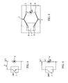
- FIG 1 (a) shows a light-emitting semiconductor device 1 comprising two terminals defined as a first terminal 2 and a second terminal 3, an LED unit 4 and a switch 7 for bypassing.
- the LED unit 4 includes several LED dice 10 as shown in FIG. 2, and has a first electrode 5 and a second electrode 6 respectively connected to the first terminal 2 and the second terminal 3.
- the circuit involving the LED unit 4 is electrically connected well and the LED dice can be lit by applying a current to the terminals 2 and 3. However, if the circuit is open, the LED unit 4 can't be lit.
- the switch 7 is made with an integrated circuit and also has a first electrode 8 and a second electrode 9 respectively connected to the terminals 2 and 3.
- the switch 7 includes a voltage detection circuit 11 and a switch circuit 12, as shown in FIG. 3.
- the switch 7 is electrically unconductible in an "Off” state, but conductible in an "On” state when triggered by a first signal received from the electrodes 8 and 9.
- This first signal is a voltage equal to or higher than a predetermined value and generated when the circuit involving the LED unit 4 is open.
- FIG 1(b) shows the LED unit 4 connected to the switch 7 through a common contact and thus controlled by the switch 7.
- the voltage detection circuit 1 has an anode, a cathode and a gate, wherein the anode and the cathode are respectively connected to the electrodes 8 and 9.
- the switch circuit 12 also has an anode, a cathode and a gate, wherein the anode and the cathode are also respectively connected to the electrodes 8 and 9.
- the gates of the circuits 11 and 12 are connected to each other. By detecting voltage of the circuit, the circuit 11 can generate a second signal to drive the gate of the switch circuit 12 through the gate of the voltage detection circuit 11. Then the switch circuit 12 enters into the "On" state.
- the switch circuit can be designed as follows:
- the bipolar junction transistor has an emitter, a base and a collector; the MOSFET has a source, a gate and a drain. The emitter and the source are respectively connected to the anode (or the cathode) and the cathode (or the anode) of the switch circuit. The base is connected to the drain. The collector is connected to the gate.
- the light-emitting semiconductor device 1 is conducted as follows:
- FIG 6 shows the electrical connection of the device.
- the electrode 5 of the LED unit 4 and the electrode 8 of the switch 7 are commonly connected to the first terminal 2 of the device 1.
- the electrode 6 of the LED unit 4 and the electrode 9 of the switch 7 are commonly connected to the second terminal 3 of the device 1.
- the terminals of the light-emitting semiconductor device can be attached to a substrate by wire bonding and surface mount technology.
- FIG 7 shows a series circuit.
- the terminal 3 of the device 1 is connected to the terminal 2' of the device 1'; and the terminal 2 of the device 1 and the terminal 3' of the device 1' are individually connected to a current source 13.
- FIG 8 shows a parallel circuit.
- the terminal 2 of the device 1 and the terminal 2' of the device 1' are commonly connected to a current source; and the terminal 3 of the device 1 and the terminal 3' of the device 1' are commonly connected to the current source. That is, the devices and the current source can form a series or parallel circuit always conductible by providing the bypass switch.
Landscapes
- Led Devices (AREA)
Applications Claiming Priority (1)
| Application Number | Priority Date | Filing Date | Title |
|---|---|---|---|
| CNB2006100015271A CN100521200C (zh) | 2006-01-18 | 2006-01-18 | 具旁路导通开关的发光半导体组件 |
Publications (1)
| Publication Number | Publication Date |
|---|---|
| EP1814366A1 true EP1814366A1 (fr) | 2007-08-01 |
Family
ID=38008053
Family Applications (1)
| Application Number | Title | Priority Date | Filing Date |
|---|---|---|---|
| EP06007984A Withdrawn EP1814366A1 (fr) | 2006-01-18 | 2006-04-18 | Dispositif à semi-conducteur émetteur de lumière comprenant un élément de dérivation détecteur de circuit ouvert |
Country Status (2)
| Country | Link |
|---|---|
| EP (1) | EP1814366A1 (fr) |
| CN (1) | CN100521200C (fr) |
Cited By (3)
| Publication number | Priority date | Publication date | Assignee | Title |
|---|---|---|---|---|
| WO2009138907A3 (fr) * | 2008-05-13 | 2010-01-07 | Nxp B.V. | Détection de pannes de dispositifs d'éclairage |
| DE102012106272A1 (de) * | 2012-07-12 | 2014-01-16 | Osram Opto Semiconductors Gmbh | Anordnung für ein optoelektronisches Bauelement und Anordnung mit einem optoelektronischen Bauelement |
| CN110798935A (zh) * | 2019-11-19 | 2020-02-14 | 深圳欧创芯半导体有限公司 | Led灯串控制方法、装置、系统及终端设备 |
Families Citing this family (4)
| Publication number | Priority date | Publication date | Assignee | Title |
|---|---|---|---|---|
| RU2562957C2 (ru) * | 2010-07-09 | 2015-09-10 | Конинклейке Филипс Электроникс Н.В. | Схема контроля для органического светоизлучающего диода |
| JP2012053387A (ja) * | 2010-09-03 | 2012-03-15 | Mitsumi Electric Co Ltd | バックライト装置、該バックライト装置を備えた表示装置及び照明装置 |
| CN112820238B (zh) * | 2019-10-30 | 2022-07-01 | 群创光电股份有限公司 | 显示器 |
| CN112967665B (zh) * | 2021-02-20 | 2023-08-15 | 厦门天马微电子有限公司 | 发光元件控制电路、显示面板和显示装置 |
Citations (6)
| Publication number | Priority date | Publication date | Assignee | Title |
|---|---|---|---|---|
| JPS6318967A (ja) * | 1986-07-11 | 1988-01-26 | Toshiba Corp | サイクロコンバ−タの制御装置 |
| JPH11178243A (ja) * | 1997-12-16 | 1999-07-02 | Mitsubishi Electric Corp | 無停電電源装置 |
| US20020043943A1 (en) * | 2000-10-10 | 2002-04-18 | Menzer Randy L. | LED array primary display light sources employing dynamically switchable bypass circuitry |
| US20040248332A1 (en) * | 2003-06-03 | 2004-12-09 | Joon Ho Yoon | Method of manufacturing light-emitting diode device |
| US20050057179A1 (en) * | 2003-08-27 | 2005-03-17 | Osram Sylvania Inc. | Driver circuit for LED vehicle lamp |
| EP1589519A2 (fr) * | 2004-04-20 | 2005-10-26 | Sony Corporation | Dispositif d'attaque à courant constant, source lumineuse pour rétroéclairage, et dispositif d'affichage couleur à cristaux liquides |
Family Cites Families (3)
| Publication number | Priority date | Publication date | Assignee | Title |
|---|---|---|---|---|
| US6323598B1 (en) * | 2000-09-29 | 2001-11-27 | Aerospace Optics, Inc. | Enhanced trim resolution voltage-controlled dimming led driver |
| CN1190070C (zh) * | 2001-04-26 | 2005-02-16 | 力捷电脑股份有限公司 | 互补金属氧化物半导体感测器中归零及读取的装置与方法 |
| KR20030096659A (ko) * | 2002-06-17 | 2003-12-31 | 삼성전자주식회사 | 이미지 센서의 화소 어레이 영역, 그 구조체 및 그 제조방법 |
-
2006
- 2006-01-18 CN CNB2006100015271A patent/CN100521200C/zh not_active Expired - Lifetime
- 2006-04-18 EP EP06007984A patent/EP1814366A1/fr not_active Withdrawn
Patent Citations (6)
| Publication number | Priority date | Publication date | Assignee | Title |
|---|---|---|---|---|
| JPS6318967A (ja) * | 1986-07-11 | 1988-01-26 | Toshiba Corp | サイクロコンバ−タの制御装置 |
| JPH11178243A (ja) * | 1997-12-16 | 1999-07-02 | Mitsubishi Electric Corp | 無停電電源装置 |
| US20020043943A1 (en) * | 2000-10-10 | 2002-04-18 | Menzer Randy L. | LED array primary display light sources employing dynamically switchable bypass circuitry |
| US20040248332A1 (en) * | 2003-06-03 | 2004-12-09 | Joon Ho Yoon | Method of manufacturing light-emitting diode device |
| US20050057179A1 (en) * | 2003-08-27 | 2005-03-17 | Osram Sylvania Inc. | Driver circuit for LED vehicle lamp |
| EP1589519A2 (fr) * | 2004-04-20 | 2005-10-26 | Sony Corporation | Dispositif d'attaque à courant constant, source lumineuse pour rétroéclairage, et dispositif d'affichage couleur à cristaux liquides |
Cited By (4)
| Publication number | Priority date | Publication date | Assignee | Title |
|---|---|---|---|---|
| WO2009138907A3 (fr) * | 2008-05-13 | 2010-01-07 | Nxp B.V. | Détection de pannes de dispositifs d'éclairage |
| DE102012106272A1 (de) * | 2012-07-12 | 2014-01-16 | Osram Opto Semiconductors Gmbh | Anordnung für ein optoelektronisches Bauelement und Anordnung mit einem optoelektronischen Bauelement |
| CN110798935A (zh) * | 2019-11-19 | 2020-02-14 | 深圳欧创芯半导体有限公司 | Led灯串控制方法、装置、系统及终端设备 |
| CN110798935B (zh) * | 2019-11-19 | 2021-10-08 | 深圳欧创芯半导体有限公司 | Led灯串控制方法、装置、系统及终端设备 |
Also Published As
| Publication number | Publication date |
|---|---|
| CN101005065A (zh) | 2007-07-25 |
| CN100521200C (zh) | 2009-07-29 |
Similar Documents
| Publication | Publication Date | Title |
|---|---|---|
| US8461670B2 (en) | Semiconductor component and method of manufacture | |
| CN101068077B (zh) | 分路保护电路及其方法 | |
| JP5991435B2 (ja) | 半導体装置 | |
| KR100276414B1 (ko) | 절연 게이트형 반도체 장치 | |
| KR960026762A (ko) | 복합형 mosfet | |
| US7916439B2 (en) | Semiconductor switch arrangement and an electronic device | |
| US10277219B2 (en) | Electronic switching and reverse polarity protection circuit | |
| US10916539B2 (en) | Semiconductor device having a transistor portion that includes an output resistive portion | |
| US20130234609A1 (en) | Led lighting device | |
| US9354269B2 (en) | Semiconductor device and method of detecting wire open failure thereof | |
| US11515868B2 (en) | Electronic circuit and semiconductor module | |
| EP1814366A1 (fr) | Dispositif à semi-conducteur émetteur de lumière comprenant un élément de dérivation détecteur de circuit ouvert | |
| CN102640419B (zh) | 半导体器件 | |
| CN108233910B (zh) | 电子电路 | |
| US9425784B2 (en) | Circuit having a power transistor and a drive circuit | |
| US8928002B2 (en) | Semiconductor device and method of manufacturing semiconductor device | |
| US20070131945A1 (en) | Light-emitting semiconductor device with open-bypass function | |
| US8410494B2 (en) | Light emitting diode package and lamp with the same | |
| US9571086B1 (en) | Bi-directional switch | |
| JPH0879041A (ja) | 光半導体リレーとこれを用いたコントローラ、電力供給装置及び端末装置切換装置 | |
| US20050122748A1 (en) | Semiconductor device and method of manufacturing thereof | |
| US7489490B2 (en) | Current limiting MOSFET structure for solid state relays | |
| JPH0918004A (ja) | 半導体集積回路 | |
| JP4710131B2 (ja) | 半導体装置 | |
| US20230420445A1 (en) | Semiconductor device and method of manufacturing semiconductor device |
Legal Events
| Date | Code | Title | Description |
|---|---|---|---|
| PUAI | Public reference made under article 153(3) epc to a published international application that has entered the european phase |
Free format text: ORIGINAL CODE: 0009012 |
|
| AK | Designated contracting states |
Kind code of ref document: A1 Designated state(s): AT BE BG CH CY CZ DE DK EE ES FI FR GB GR HU IE IS IT LI LT LU LV MC NL PL PT RO SE SI SK TR |
|
| AX | Request for extension of the european patent |
Extension state: AL BA HR MK YU |
|
| 17P | Request for examination filed |
Effective date: 20080131 |
|
| 17Q | First examination report despatched |
Effective date: 20080303 |
|
| AKX | Designation fees paid |
Designated state(s): BE DE GB IT |
|
| STAA | Information on the status of an ep patent application or granted ep patent |
Free format text: STATUS: THE APPLICATION IS DEEMED TO BE WITHDRAWN |
|
| 18D | Application deemed to be withdrawn |
Effective date: 20110127 |