EP1815295B1 - Reseau de modulateurs spatiaux de lumiere et procede de production d'un dispositif a modulateurs spatiaux de lumiere - Google Patents
Reseau de modulateurs spatiaux de lumiere et procede de production d'un dispositif a modulateurs spatiaux de lumiere Download PDFInfo
- Publication number
- EP1815295B1 EP1815295B1 EP05805199A EP05805199A EP1815295B1 EP 1815295 B1 EP1815295 B1 EP 1815295B1 EP 05805199 A EP05805199 A EP 05805199A EP 05805199 A EP05805199 A EP 05805199A EP 1815295 B1 EP1815295 B1 EP 1815295B1
- Authority
- EP
- European Patent Office
- Prior art keywords
- substrate
- spatial light
- light modulator
- slm
- slms
- Prior art date
- Legal status (The legal status is an assumption and is not a legal conclusion. Google has not performed a legal analysis and makes no representation as to the accuracy of the status listed.)
- Expired - Lifetime
Links
Images



Classifications
-
- B—PERFORMING OPERATIONS; TRANSPORTING
- B81—MICROSTRUCTURAL TECHNOLOGY
- B81C—PROCESSES OR APPARATUS SPECIALLY ADAPTED FOR THE MANUFACTURE OR TREATMENT OF MICROSTRUCTURAL DEVICES OR SYSTEMS
- B81C1/00—Manufacture or treatment of devices or systems in or on a substrate
-
- G—PHYSICS
- G03—PHOTOGRAPHY; CINEMATOGRAPHY; ANALOGOUS TECHNIQUES USING WAVES OTHER THAN OPTICAL WAVES; ELECTROGRAPHY; HOLOGRAPHY
- G03F—PHOTOMECHANICAL PRODUCTION OF TEXTURED OR PATTERNED SURFACES, e.g. FOR PRINTING, FOR PROCESSING OF SEMICONDUCTOR DEVICES; MATERIALS THEREFOR; ORIGINALS THEREFOR; APPARATUS SPECIALLY ADAPTED THEREFOR
- G03F7/00—Photomechanical, e.g. photolithographic, production of textured or patterned surfaces, e.g. printing surfaces; Materials therefor, e.g. comprising photoresists; Apparatus specially adapted therefor
- G03F7/70—Microphotolithographic exposure; Apparatus therefor
- G03F7/70216—Mask projection systems
- G03F7/70283—Mask effects on the imaging process
-
- B—PERFORMING OPERATIONS; TRANSPORTING
- B81—MICROSTRUCTURAL TECHNOLOGY
- B81C—PROCESSES OR APPARATUS SPECIALLY ADAPTED FOR THE MANUFACTURE OR TREATMENT OF MICROSTRUCTURAL DEVICES OR SYSTEMS
- B81C3/00—Assembling of devices or systems from individually processed components
-
- G—PHYSICS
- G02—OPTICS
- G02B—OPTICAL ELEMENTS, SYSTEMS OR APPARATUS
- G02B26/00—Optical devices or arrangements for the control of light using movable or deformable optical elements
-
- G—PHYSICS
- G03—PHOTOGRAPHY; CINEMATOGRAPHY; ANALOGOUS TECHNIQUES USING WAVES OTHER THAN OPTICAL WAVES; ELECTROGRAPHY; HOLOGRAPHY
- G03F—PHOTOMECHANICAL PRODUCTION OF TEXTURED OR PATTERNED SURFACES, e.g. FOR PRINTING, FOR PROCESSING OF SEMICONDUCTOR DEVICES; MATERIALS THEREFOR; ORIGINALS THEREFOR; APPARATUS SPECIALLY ADAPTED THEREFOR
- G03F7/00—Photomechanical, e.g. photolithographic, production of textured or patterned surfaces, e.g. printing surfaces; Materials therefor, e.g. comprising photoresists; Apparatus specially adapted therefor
- G03F7/70—Microphotolithographic exposure; Apparatus therefor
- G03F7/70216—Mask projection systems
- G03F7/70283—Mask effects on the imaging process
- G03F7/70291—Addressable masks, e.g. spatial light modulators [SLMs], digital micro-mirror devices [DMDs] or liquid crystal display [LCD] patterning devices
-
- G—PHYSICS
- G03—PHOTOGRAPHY; CINEMATOGRAPHY; ANALOGOUS TECHNIQUES USING WAVES OTHER THAN OPTICAL WAVES; ELECTROGRAPHY; HOLOGRAPHY
- G03F—PHOTOMECHANICAL PRODUCTION OF TEXTURED OR PATTERNED SURFACES, e.g. FOR PRINTING, FOR PROCESSING OF SEMICONDUCTOR DEVICES; MATERIALS THEREFOR; ORIGINALS THEREFOR; APPARATUS SPECIALLY ADAPTED THEREFOR
- G03F7/00—Photomechanical, e.g. photolithographic, production of textured or patterned surfaces, e.g. printing surfaces; Materials therefor, e.g. comprising photoresists; Apparatus specially adapted therefor
- G03F7/70—Microphotolithographic exposure; Apparatus therefor
- G03F7/708—Construction of apparatus, e.g. environment aspects, hygiene aspects or materials
- G03F7/70808—Construction details, e.g. housing, load-lock, seals or windows for passing light in or out of apparatus
- G03F7/70825—Mounting of individual elements, e.g. mounts, holders or supports
-
- Y—GENERAL TAGGING OF NEW TECHNOLOGICAL DEVELOPMENTS; GENERAL TAGGING OF CROSS-SECTIONAL TECHNOLOGIES SPANNING OVER SEVERAL SECTIONS OF THE IPC; TECHNICAL SUBJECTS COVERED BY FORMER USPC CROSS-REFERENCE ART COLLECTIONS [XRACs] AND DIGESTS
- Y10—TECHNICAL SUBJECTS COVERED BY FORMER USPC
- Y10T—TECHNICAL SUBJECTS COVERED BY FORMER US CLASSIFICATION
- Y10T29/00—Metal working
- Y10T29/49—Method of mechanical manufacture
- Y10T29/49826—Assembling or joining
Definitions
- the invention relates to an array of spatial light modulators and a method of production of a spatial light modulator device. More specifically, it relates to arrays of spatial light modulators as can be used in maskless lithography systems
- lithographic technologies are used.
- the most common approaches are based on the step-principle or on the step-and-scan-principle. Both approaches are working with masks providing the structure to be projected onto a substrate.
- the masks have to show a high degree of accuracy and are very expensive.
- SLMs programmable spatial light modulators
- a SLM comprises a multitude of units like deformable mirror-devices or liquid crystal light valves, each corresponding to a pixel of the structure to be illuminated. Every pixel can be switched between the two states, i.e. illuminating or not illuminating the corresponding point on the wafer surface.
- Some SLMs have units with also an intermediate state, illuminating the corresponding point on the substrate surface with an intermediate intensity.
- the digitalized structure to be projected is provided by a control unit, that controls every pixel and can switch the corresponding unit into the necessary state. If the structure to be projected is changed, the states of the units of the SLM are changed, too, where necessary.
- a plurality of SLMs have to be arranged in a planar configuration with very tight specifications in terms of x- and y-position and planarity.
- the document EP 1 162 169 A2 describes methods for interconnecting microelectronic machined mechanical systems (MEMS).
- the substrate of choice for a MEMS device is typically a semi-conductor wafer e.g. silicon.
- a micro-mechanical mirror array is produced according to this document by mounting an array of MEMS devices on a silicon substrate.
- a silicon chamber can be provided to enclose the MEMS devices.
- the individual wafers are therefore prepared with large openings to accommodate the MEMS devices.
- the document US 2004/0130561 discloses a mask-less lithography system with multiplexed spatial light modulators.
- the spatial light modulators are arranged in twin planes on a substrate, such that the chip kerf and connector fan-in regions overlap substantially.
- the document EP 1 369 730 A1 describes flip-chip fabrication of a micromirror unit which has a mirror substrate and a wiring substrate that is spaced by conductive spacers.
- the document EP 1 280 007 describes an imaging apparatus that comprises a support structure for supporting patterning means.
- the patterning means serve to pattern the projection beam generated by a radiation system according to a desired pattern.
- a patterning means comprises a plurality of separate patterning sub-elements. Each sub-element is used to generate a patterned sub-beam.
- the apparatus furthermore comprises combining means for combining the plurality of patterned sub-beams into a single patterned image.
- a method according to claim 1 for the production of a SLM device comprising the step of mounting a spatial light modulator on a substrate of the same material as the main material of the SLM array to be juxtaposed with the substrate.
- a spatial light modulator on a substrate of the same material as the main material of the SLM array to be juxtaposed with the substrate.
- silicon based SLMs are mounted on a silicon substrate.
- a SLM device may comprise a single or a plurality of SLMs, leading to an array of SLMs.
- the present invention is independent of the number of SLMs used and works as well for a single SLM array as for a plurality of SLMs.
- the substrate material leads to a perfect thermal match of substrate and SLM. This is a very important step in achieving the severe specifications with respect to position and planarity for use in a maskless lithography system.
- impinging photons deposit energy in the SLM device inducing a substantial thermal load.
- Different coefficients of thermal expansion of the substrate and the SLMs would lead to major deformations of the SLM device, thus making it eventually impossible to reach the specifications.
- the substrate material to match the material of the SLMs specifically the main material to be juxtaposed with the substrate, e.g. a carrier substrate of the SLM itself, both substrate and SLM behave in the same way, when heated, such that only a scale effect with respect to x- and y-positions has to be taken into account during illumination, but no deformations.
- the SLM is mounted by using surface mount technology, preferably by soldering.
- This has the advantage, especially if using a solder with high surface tension, that the self-aligning effect of solder during reflow due to minimizing the surface energy of the solder provides SLM devices of low variation with respect to position and planarity. This helps meeting the severe specifications and lowers production cost.
- the substrate is preformed to provide it with an opening for exposing the SLM.
- the substrate is preformed to provide it with an opening for exposing the SLM.
- the substrate is provided with the infrastructure for the SLM such as electronic circuits, connectors etc..
- the other side can be processed to be optimized for optical use like having a defined reflection or absorption characteristic.
- the optically active side of the SLM is oriented such that it is exposed to the light, when being illuminated, as well as the side of the substrate optimized for optical use, while all the infrastructure is on the other side of the substrate.
- an array of SLMs on a substrate wherein the substrate is of the same material as the main material of the SLMs to be juxtaposed with the substrate.
- the SLMs may be mounted on the substrate by means of solder-defined self-aligning connections and are arranged in flip-chip geometry, the substrate having openings for exposing the SLMs, the infrastructure for the SLMs being provided on one side of the substrate, while the other side has a defined reflection or absorption function.
- a maskless lithography system with such an array of SLMs is provided.
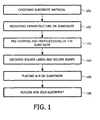
- Figure 1 shows an embodiment of the production method according to the invention.
- a first step 101 one has to choose the appropriate material for the substrate depending on the SLM to be mounted on the substrate.
- Most SLMs are semiconductor devices, i.e. the SLM is arranged on a carrier substrate.
- This carrier substrate is the part of the SLM that will actually be juxtaposed with the substrate. Therefore, the substrate material is to be chosen to be the same as the material of the carrier substrate to get a perfect thermal match.
- the side of the substrate opposite to the light side is provided with all the necessary infrastructure for the SLM, e.g. flex connections, preamplifiers, electrical circuitry, thin film interconnects, connection pads, microconnectors etc..
- SLM simple metal-oxide-semiconductor
- Some components have to be quite near to the SLM like preamplifiers, whereas other components can be farther away and connected with the SLM by thin film interconnects and/or flex connectors.
- the substrate is pre-formed (step 103) to provide it with an opening corresponding to the size of the optically active surface of the SLM to be used, and preprocessed to provide one side of the substrate (so-called light side) with a finishing layer for providing defined absorption or reflection characteristics.
- the finishing layer is an anti-reflection layer, such as for example a chromium oxide layer as is used on photomasks.
- a UV light absorbing layer especially an absorbing polymer layer as is used in integrated circuit fabrication processes.
- step 104 the solder lands are accurately defined and the solder bumps carefully controlled, before placing substrate and SLM accurately together in step 105.
- the solder lands or solderable interconnect pads are defined on both the substrate and the carrier substrate of the SLM, whereas the solder bumps are placed only on the solder lands of either the substrate or the SLM.
- Solder lands are accurately defined by etching windows in e.g. a silicon nitride passivation layer on the substrate, using photolithography and reactive ion etching.
- a solder with high surface tension is used. Very much preferred are solders, which have a high tin content.
- the last step 106 is the reflow leading to self-alignment of the SLM with respect to the substrate.
- One possible reflow process could be the following: First, the SLM device is preheated to gradually heat it up. The device is then kept at a temperature near to the temperature at which solder bonding can occur till all parts of the SLM device have reached the same temperature. The actual reflow is, when the device is heated to a temperature above the melting point of the solder for bonding. Afterwards, the SLM device is cooled evenly to avoid thermal shock. The reflow process may occur in an inert or eventually reducing atmosphere, in order to prevent oxidation of the solder bumps, which in turn would hamper the self-aligning process.
- FIGS 2a and 2b show a SLM 2 and a substrate 3. Both SLM 2 and substrate 3 are provided with solder lands 21 and are in contact via solder bumps 22.
- Figure 2a is shown the state before reflow, in which SLM 2 and substrate 3 are poorly aligned.
- the solder bumps 22 become liquid, due to minimization of free energy, the free surface of the solder bumps 22 is minimized. This leads to accurate alignment of the substrate 3 and the SLM 2.
- the alignment is not only reached for the displacement in the XY-plane, but also for the rotation in the XY-plane and the out-of-plane rotation.
- Figure 3 shows a SLM 2 on silicon basis mounted onto a silicon substrate 3.
- the SLM 2 is arranged in flip-chip geometry on the substrate 3, such that the optically active side of the SLM 2 is exposed to the illuminating light beam 4 through the opening 32.
- the side 6 of the substrate 3 that is exposed to the light 4 is the light side 6.
- a finishing layer 30 has been deposited on the light side 6 of the substrate 3 to provide defined absorption or reflection characteristics.
- the dark side 5 the SLM 2 is fixed to the substrate 3 by solder connections 20.
- the SLM shown in Figure 3 is used in reflection mode and is based on micro-mirror devices.
- the infrastructure for the SLM 2 is provided on the dark side 5, e.g. a preamplifier 11, flex connections 10, that can be oriented in any direction, fine pitch thin film interconnects 13 and electrical circuitry 12.
- Dividing the SLM device into a light side 6 and a dark side 5 has two major advantages: The infrastructure is protected from the illuminating light 4, and the infrastructure does not impede the imaging process, as it is hidden.
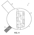
- Figure 4 shows the light side of an array I of SLMs 2.
- the SLMs 2 are arranged in an optically active area 31 of the substrate 3, that is actually to be illuminated.
- the substrate 3 has an antireflection or absorbing finishing layer 30 to make sure, that any structure to be projected on e.g. a wafer is due only to the SLMs 2 and not to any stray reflects of the substrate.
- the normal flex connection 10 and the micro-fine pitch connection 14 are the only parts of the infrastructure from the dark side of the substrate 3 that are visible, but very far away from the optically active area 31.
- the SLMs 2 of the optically active area 31 are arranged in an irregular manner in Figure 4 .
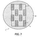
- the invention is applicable to any arrangement of SLMs, e.g. to a regular arrays 1 as illustrated in Figure 7 .
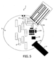
- Figure 5 shows the dark side of an array 1 of SLMs 2.
- SLMs 2 diverse components operating as infrastructure for the SLMs 2 are mounted on the substrate 3.
- a flex connection 10 connecting the SLMs 2 via fine pitch thin film interconnects 13 and pads 15a with a control unit, e.g. a computer, where the structure data to be implemented by the SLMs 2 is provided, circuitry 12 connected via connecting pads 15b, and micro-connectors 16, e.g. for connecting micro-fine pitch connections 14.
- Figure 6 sketches a basic maskless lithography system 7.
- Light 4 is emitted by a light source 40.
- the illuminating system optimizes the light 4 for illumination of the array 1 of SLMs.
- the array 1 is used in transmission with SLMs based on liquid crystal light valve devices.
- the light 4 transmitted by the array 1 of SLMs is projected on the wafer 43 for imaging with the help of a projection system 42.
Landscapes
- Physics & Mathematics (AREA)
- General Physics & Mathematics (AREA)
- Engineering & Computer Science (AREA)
- Public Health (AREA)
- Environmental & Geological Engineering (AREA)
- Epidemiology (AREA)
- Health & Medical Sciences (AREA)
- Microelectronics & Electronic Packaging (AREA)
- Manufacturing & Machinery (AREA)
- Optics & Photonics (AREA)
- Liquid Crystal (AREA)
- Exposure And Positioning Against Photoresist Photosensitive Materials (AREA)
- Mechanical Light Control Or Optical Switches (AREA)
- Wire Bonding (AREA)
Claims (14)
- Procédé de production d'un dispositif de modulateur spatial de lumière comprenant l'étape consistant à monter un modulateur spatial de lumière (2) sur un substrat (3) qui se compose du même matériau que le matériau principal du modulateur spatial de lumière à juxtaposer avec le substrat, caractérisé en ce que le substrat présente une ouverture (32) pour exposer le modulateur spatial de lumière et en ce que le modulateur spatial de lumière est agencé dans une géométrie dite flip-chip sur le substrat.
- Procédé selon la revendication 1, dans lequel le modulateur spatial de lumière à base de silicium est monté sur un substrat de silicium.
- Procédé selon la revendication 1 ou 2, comprenant la nouvelle autre étape consistant à monter le modulateur spatial de lumière sur le substrat à l'aide de la technologie de montage en surface.
- Procédé selon la revendication 1, 2 ou 3, comprenant la nouvelle autre étape consistant à monter le modulateur spatial de lumière sur le substrat par soudage.
- Procédé selon l'une quelconque des revendications précédentes 1 à 4, comprenant la nouvelle autre étape consistant à monter le modulateur spatial de lumière sur le substrat en définissant des parties intermédiaires de soudage et des perles de soudure, en assemblant le modulateur spatial de lumière et en faisant usage de l'effet de minimisation de la surface libre des perles de soudure pendant le reflux pour l'alignement automatique du modulateur spatial de lumière par rapport au substrat.
- Procédé selon la revendication 3, 4 ou 5, dans lequel une soudure à haute tension de surface est utilisée.
- Procédé selon l'une quelconque des revendications précédentes 3 à 6, dans lequel une soudure à haute teneur en étain est utilisée.
- Procédé selon l'une quelconque des revendications précédentes 1 à 7, comprenant la nouvelle autre étape consistant à préformer le substrat de manière à pourvoir le substrat d'une ouverture pour exposer le modulateur spatial de lumière.
- Procédé selon l'une quelconque des revendications précédentes 1 à 8, comprenant la nouvelle autre étape consistant à fournir l'infrastructure pour le modulateur spatial de lumière d'un seul côté du substrat.
- Procédé selon l'une quelconque des revendications précédentes 1 à 9, comprenant la nouvelle autre étape consistant à traiter l'autre côté du substrat de manière à atteindre une réflexion ou une absorption définie.
- Réseau (1) de modulateurs spatiaux de lumière (2) sur un substrat (3), dans lequel le substrat (3) se compose du même matériau que le matériau principal des modulateurs spatiaux de lumière (2) à juxtaposer avec le substrat (3), caractérisé en ce que le substrat (3) présente des ouvertures (32) pour exposer les modulateurs spatiaux de lumière et en ce que les modulateurs spatiaux de lumière (2) sont agencés dans une géométrie dite flip-chip.
- Réseau selon la revendication 11, dans lequel les modulateurs spatiaux de lumière (2) sont montés sur le substrat (3) au moyen de raccordements d'alignement automatique définis par soudure (20).
- Réseau selon la revendication 11 ou 12, dans lequel l'infrastructure (10, 11, 12, 13, 14, 15a, b, 16) pour le modulateur spatial de lumière (2) est prévue d'un côté (5) du substrat (3) alors que l'autre côté (6) présente une fonction de réflexion ou d'absorption définie.
- Système de gravure sans masque (7) avec un réseau (1) de modulateurs spatiaux de lumière selon la revendication 11, 12 ou 13.
Priority Applications (1)
| Application Number | Priority Date | Filing Date | Title |
|---|---|---|---|
| EP05805199A EP1815295B1 (fr) | 2004-11-09 | 2005-11-03 | Reseau de modulateurs spatiaux de lumiere et procede de production d'un dispositif a modulateurs spatiaux de lumiere |
Applications Claiming Priority (3)
| Application Number | Priority Date | Filing Date | Title |
|---|---|---|---|
| EP04105607 | 2004-11-09 | ||
| EP05805199A EP1815295B1 (fr) | 2004-11-09 | 2005-11-03 | Reseau de modulateurs spatiaux de lumiere et procede de production d'un dispositif a modulateurs spatiaux de lumiere |
| PCT/IB2005/053588 WO2006051448A2 (fr) | 2004-11-09 | 2005-11-03 | Reseau de modulateurs spatiaux de lumiere et procede de production d'un dispositif a modulateurs spatiaux de lumiere |
Publications (2)
| Publication Number | Publication Date |
|---|---|
| EP1815295A2 EP1815295A2 (fr) | 2007-08-08 |
| EP1815295B1 true EP1815295B1 (fr) | 2008-12-03 |
Family
ID=35539572
Family Applications (1)
| Application Number | Title | Priority Date | Filing Date |
|---|---|---|---|
| EP05805199A Expired - Lifetime EP1815295B1 (fr) | 2004-11-09 | 2005-11-03 | Reseau de modulateurs spatiaux de lumiere et procede de production d'un dispositif a modulateurs spatiaux de lumiere |
Country Status (9)
| Country | Link |
|---|---|
| US (1) | US20090040595A1 (fr) |
| EP (1) | EP1815295B1 (fr) |
| JP (1) | JP2008521024A (fr) |
| KR (1) | KR20070083985A (fr) |
| CN (1) | CN100524037C (fr) |
| AT (1) | ATE416398T1 (fr) |
| DE (1) | DE602005011475D1 (fr) |
| TW (1) | TW200630758A (fr) |
| WO (1) | WO2006051448A2 (fr) |
Families Citing this family (6)
| Publication number | Priority date | Publication date | Assignee | Title |
|---|---|---|---|---|
| US8064122B2 (en) | 2007-03-15 | 2011-11-22 | Asml Holding N.V. | Apertured window for enabling flexible illumination overfill of patterning devices |
| HRP20180233T1 (hr) * | 2011-05-13 | 2018-06-01 | Euro-Celtique S.A. | Intranazalni farmaceutski oblici doziranja koji sadrže nalokson |
| KR102151254B1 (ko) | 2013-08-19 | 2020-09-03 | 삼성디스플레이 주식회사 | 노광장치 및 그 방법 |
| CN216873443U (zh) | 2019-01-04 | 2022-07-01 | 恩格特公司 | 精确对准的组件 |
| US11872760B2 (en) | 2020-10-29 | 2024-01-16 | Seurat Technologies, Inc. | Distributed flux array |
| WO2022115197A2 (fr) * | 2020-10-29 | 2022-06-02 | Seurat Technologies, Inc. | Système de refroidissement de valve lumineuse |
Family Cites Families (10)
| Publication number | Priority date | Publication date | Assignee | Title |
|---|---|---|---|---|
| US5311360A (en) * | 1992-04-28 | 1994-05-10 | The Board Of Trustees Of The Leland Stanford, Junior University | Method and apparatus for modulating a light beam |
| US5406906A (en) * | 1994-01-18 | 1995-04-18 | Ford Motor Company | Preparation of crystallographically aligned films of silicon carbide by laser deposition of carbon onto silicon |
| US6466349B1 (en) * | 1998-05-14 | 2002-10-15 | Hughes Electronics Corporation | Integrated optical transmitter |
| FR2789801B1 (fr) * | 1999-02-12 | 2001-04-27 | Thomson Tubes Electroniques | Cathode a effet de champ a performances accrues |
| US6396711B1 (en) | 2000-06-06 | 2002-05-28 | Agere Systems Guardian Corp. | Interconnecting micromechanical devices |
| US6602427B1 (en) * | 2000-08-28 | 2003-08-05 | Xiang Zheng Tu | Micromachined optical mechanical modulator based transmitter/receiver module |
| EP1280007B1 (fr) | 2001-07-24 | 2008-06-18 | ASML Netherlands B.V. | Appareil pour la production des images |
| US6522793B1 (en) * | 2001-11-21 | 2003-02-18 | Andrei Szilagyi | Low voltage electro-optic modulator with integrated driver |
| JP4140816B2 (ja) | 2002-05-24 | 2008-08-27 | 富士通株式会社 | マイクロミラー素子 |
| US6870554B2 (en) * | 2003-01-07 | 2005-03-22 | Anvik Corporation | Maskless lithography with multiplexed spatial light modulators |
-
2005
- 2005-11-03 DE DE602005011475T patent/DE602005011475D1/de not_active Expired - Fee Related
- 2005-11-03 CN CNB2005800382005A patent/CN100524037C/zh not_active Expired - Fee Related
- 2005-11-03 US US11/718,405 patent/US20090040595A1/en not_active Abandoned
- 2005-11-03 JP JP2007539685A patent/JP2008521024A/ja not_active Withdrawn
- 2005-11-03 KR KR1020077010216A patent/KR20070083985A/ko not_active Withdrawn
- 2005-11-03 EP EP05805199A patent/EP1815295B1/fr not_active Expired - Lifetime
- 2005-11-03 WO PCT/IB2005/053588 patent/WO2006051448A2/fr not_active Ceased
- 2005-11-03 AT AT05805199T patent/ATE416398T1/de not_active IP Right Cessation
- 2005-11-04 TW TW094138850A patent/TW200630758A/zh unknown
Also Published As
| Publication number | Publication date |
|---|---|
| CN101057184A (zh) | 2007-10-17 |
| EP1815295A2 (fr) | 2007-08-08 |
| ATE416398T1 (de) | 2008-12-15 |
| TW200630758A (en) | 2006-09-01 |
| KR20070083985A (ko) | 2007-08-24 |
| WO2006051448A2 (fr) | 2006-05-18 |
| WO2006051448A3 (fr) | 2006-12-21 |
| US20090040595A1 (en) | 2009-02-12 |
| CN100524037C (zh) | 2009-08-05 |
| DE602005011475D1 (de) | 2009-01-15 |
| JP2008521024A (ja) | 2008-06-19 |
Similar Documents
| Publication | Publication Date | Title |
|---|---|---|
| US5716759A (en) | Method and apparatus for producing integrated circuit devices | |
| US9791691B2 (en) | Mirror array | |
| KR101895825B1 (ko) | 조명 장치, 조명 방법, 노광 장치, 노광 방법 및 디바이스 제조 방법 | |
| KR102395621B1 (ko) | 직접 기입 마스크리스 리소그래피를 위한 방법 및 장치 | |
| CN104380202B (zh) | 光学部件 | |
| TW529172B (en) | Imaging apparatus | |
| WO2018015113A1 (fr) | Procédé de lithographie sans masque à écriture directe | |
| HK1223680A1 (zh) | 照明光学系统、照明方法、曝光装置以及曝光方法 | |
| TWI913588B (zh) | 用於基於mems之微反射鏡的應力降低安裝的裝置、光學部件、光學組合件以及用於產生此裝置的方法 | |
| KR20180099834A (ko) | 직접 기입 마스크리스 리소그래피를 위한 방법 및 장치 | |
| JP5530424B2 (ja) | 光学素子を支持する装置、及びそれを形成する方法 | |
| US20250199414A1 (en) | Microelectromechanical device | |
| US20090040595A1 (en) | Array of spatial light modulators an dmethod of production of a spatial light modulator device | |
| US20040214483A1 (en) | Driving apparatus, optical system, exposure apparatus and device fabrication method | |
| TW202232046A (zh) | 微機電系統陣列互連設計 | |
| US11143965B2 (en) | Optical lithography system for patterning semiconductor devices and method of using the same | |
| EP1768183A2 (fr) | Microdispositifs avec contacts à protubérance sur ses deux faces et son procédé de fabrication | |
| US6243159B1 (en) | Projection aligner and exposure method using the same | |
| JP7625950B2 (ja) | 露光装置、露光方法、デバイス製造方法、及びデバイス | |
| Fay et al. | Advanced X-ray alignment system | |
| US12619157B2 (en) | Optical lithography system and method of using the same | |
| US20040165163A1 (en) | [substrate exposure apparatus and method] | |
| WO2005083522A1 (fr) | Procédé de formation d’un schéma | |
| JP2000340741A (ja) | マルチチップモジュールの製造方法および製造装置 | |
| JP2000260690A (ja) | X線露光装置 |
Legal Events
| Date | Code | Title | Description |
|---|---|---|---|
| PUAI | Public reference made under article 153(3) epc to a published international application that has entered the european phase |
Free format text: ORIGINAL CODE: 0009012 |
|
| 17P | Request for examination filed |
Effective date: 20070621 |
|
| AK | Designated contracting states |
Kind code of ref document: A2 Designated state(s): AT BE BG CH CY CZ DE DK EE ES FI FR GB GR HU IE IS IT LI LT LU LV MC NL PL PT RO SE SI SK TR |
|
| 17Q | First examination report despatched |
Effective date: 20071026 |
|
| DAX | Request for extension of the european patent (deleted) | ||
| GRAP | Despatch of communication of intention to grant a patent |
Free format text: ORIGINAL CODE: EPIDOSNIGR1 |
|
| GRAS | Grant fee paid |
Free format text: ORIGINAL CODE: EPIDOSNIGR3 |
|
| GRAA | (expected) grant |
Free format text: ORIGINAL CODE: 0009210 |
|
| AK | Designated contracting states |
Kind code of ref document: B1 Designated state(s): AT BE BG CH CY CZ DE DK EE ES FI FR GB GR HU IE IS IT LI LT LU LV MC NL PL PT RO SE SI SK TR |
|
| REG | Reference to a national code |
Ref country code: GB Ref legal event code: FG4D |
|
| REG | Reference to a national code |
Ref country code: CH Ref legal event code: EP |
|
| REG | Reference to a national code |
Ref country code: IE Ref legal event code: FG4D |
|
| REF | Corresponds to: |
Ref document number: 602005011475 Country of ref document: DE Date of ref document: 20090115 Kind code of ref document: P |
|
| PG25 | Lapsed in a contracting state [announced via postgrant information from national office to epo] |
Ref country code: LT Free format text: LAPSE BECAUSE OF FAILURE TO SUBMIT A TRANSLATION OF THE DESCRIPTION OR TO PAY THE FEE WITHIN THE PRESCRIBED TIME-LIMIT Effective date: 20081203 Ref country code: ES Free format text: LAPSE BECAUSE OF FAILURE TO SUBMIT A TRANSLATION OF THE DESCRIPTION OR TO PAY THE FEE WITHIN THE PRESCRIBED TIME-LIMIT Effective date: 20090314 |
|
| NLV1 | Nl: lapsed or annulled due to failure to fulfill the requirements of art. 29p and 29m of the patents act | ||
| PG25 | Lapsed in a contracting state [announced via postgrant information from national office to epo] |
Ref country code: FI Free format text: LAPSE BECAUSE OF FAILURE TO SUBMIT A TRANSLATION OF THE DESCRIPTION OR TO PAY THE FEE WITHIN THE PRESCRIBED TIME-LIMIT Effective date: 20081203 Ref country code: NL Free format text: LAPSE BECAUSE OF FAILURE TO SUBMIT A TRANSLATION OF THE DESCRIPTION OR TO PAY THE FEE WITHIN THE PRESCRIBED TIME-LIMIT Effective date: 20081203 Ref country code: PL Free format text: LAPSE BECAUSE OF FAILURE TO SUBMIT A TRANSLATION OF THE DESCRIPTION OR TO PAY THE FEE WITHIN THE PRESCRIBED TIME-LIMIT Effective date: 20081203 Ref country code: LV Free format text: LAPSE BECAUSE OF FAILURE TO SUBMIT A TRANSLATION OF THE DESCRIPTION OR TO PAY THE FEE WITHIN THE PRESCRIBED TIME-LIMIT Effective date: 20081203 Ref country code: SI Free format text: LAPSE BECAUSE OF FAILURE TO SUBMIT A TRANSLATION OF THE DESCRIPTION OR TO PAY THE FEE WITHIN THE PRESCRIBED TIME-LIMIT Effective date: 20081203 |
|
| PG25 | Lapsed in a contracting state [announced via postgrant information from national office to epo] |
Ref country code: EE Free format text: LAPSE BECAUSE OF FAILURE TO SUBMIT A TRANSLATION OF THE DESCRIPTION OR TO PAY THE FEE WITHIN THE PRESCRIBED TIME-LIMIT Effective date: 20081203 Ref country code: BE Free format text: LAPSE BECAUSE OF FAILURE TO SUBMIT A TRANSLATION OF THE DESCRIPTION OR TO PAY THE FEE WITHIN THE PRESCRIBED TIME-LIMIT Effective date: 20081203 Ref country code: RO Free format text: LAPSE BECAUSE OF FAILURE TO SUBMIT A TRANSLATION OF THE DESCRIPTION OR TO PAY THE FEE WITHIN THE PRESCRIBED TIME-LIMIT Effective date: 20081203 Ref country code: BG Free format text: LAPSE BECAUSE OF FAILURE TO SUBMIT A TRANSLATION OF THE DESCRIPTION OR TO PAY THE FEE WITHIN THE PRESCRIBED TIME-LIMIT Effective date: 20090303 |
|
| PG25 | Lapsed in a contracting state [announced via postgrant information from national office to epo] |
Ref country code: SE Free format text: LAPSE BECAUSE OF FAILURE TO SUBMIT A TRANSLATION OF THE DESCRIPTION OR TO PAY THE FEE WITHIN THE PRESCRIBED TIME-LIMIT Effective date: 20090303 Ref country code: PT Free format text: LAPSE BECAUSE OF FAILURE TO SUBMIT A TRANSLATION OF THE DESCRIPTION OR TO PAY THE FEE WITHIN THE PRESCRIBED TIME-LIMIT Effective date: 20090504 Ref country code: AT Free format text: LAPSE BECAUSE OF FAILURE TO SUBMIT A TRANSLATION OF THE DESCRIPTION OR TO PAY THE FEE WITHIN THE PRESCRIBED TIME-LIMIT Effective date: 20081203 Ref country code: CZ Free format text: LAPSE BECAUSE OF FAILURE TO SUBMIT A TRANSLATION OF THE DESCRIPTION OR TO PAY THE FEE WITHIN THE PRESCRIBED TIME-LIMIT Effective date: 20081203 Ref country code: IS Free format text: LAPSE BECAUSE OF FAILURE TO SUBMIT A TRANSLATION OF THE DESCRIPTION OR TO PAY THE FEE WITHIN THE PRESCRIBED TIME-LIMIT Effective date: 20090403 |
|
| PG25 | Lapsed in a contracting state [announced via postgrant information from national office to epo] |
Ref country code: SK Free format text: LAPSE BECAUSE OF FAILURE TO SUBMIT A TRANSLATION OF THE DESCRIPTION OR TO PAY THE FEE WITHIN THE PRESCRIBED TIME-LIMIT Effective date: 20081203 |
|
| PLBE | No opposition filed within time limit |
Free format text: ORIGINAL CODE: 0009261 |
|
| STAA | Information on the status of an ep patent application or granted ep patent |
Free format text: STATUS: NO OPPOSITION FILED WITHIN TIME LIMIT |
|
| PG25 | Lapsed in a contracting state [announced via postgrant information from national office to epo] |
Ref country code: DK Free format text: LAPSE BECAUSE OF FAILURE TO SUBMIT A TRANSLATION OF THE DESCRIPTION OR TO PAY THE FEE WITHIN THE PRESCRIBED TIME-LIMIT Effective date: 20081203 |
|
| 26N | No opposition filed |
Effective date: 20090904 |
|
| PG25 | Lapsed in a contracting state [announced via postgrant information from national office to epo] |
Ref country code: MC Free format text: LAPSE BECAUSE OF NON-PAYMENT OF DUE FEES Effective date: 20091130 |
|
| REG | Reference to a national code |
Ref country code: CH Ref legal event code: PL |
|
| GBPC | Gb: european patent ceased through non-payment of renewal fee |
Effective date: 20091103 |
|
| REG | Reference to a national code |
Ref country code: FR Ref legal event code: ST Effective date: 20100730 |
|
| PG25 | Lapsed in a contracting state [announced via postgrant information from national office to epo] |
Ref country code: IE Free format text: LAPSE BECAUSE OF NON-PAYMENT OF DUE FEES Effective date: 20091103 Ref country code: GR Free format text: LAPSE BECAUSE OF FAILURE TO SUBMIT A TRANSLATION OF THE DESCRIPTION OR TO PAY THE FEE WITHIN THE PRESCRIBED TIME-LIMIT Effective date: 20090304 Ref country code: FR Free format text: LAPSE BECAUSE OF NON-PAYMENT OF DUE FEES Effective date: 20091130 Ref country code: CH Free format text: LAPSE BECAUSE OF NON-PAYMENT OF DUE FEES Effective date: 20091130 Ref country code: LI Free format text: LAPSE BECAUSE OF NON-PAYMENT OF DUE FEES Effective date: 20091130 |
|
| PG25 | Lapsed in a contracting state [announced via postgrant information from national office to epo] |
Ref country code: DE Free format text: LAPSE BECAUSE OF NON-PAYMENT OF DUE FEES Effective date: 20100601 |
|
| PG25 | Lapsed in a contracting state [announced via postgrant information from national office to epo] |
Ref country code: GB Free format text: LAPSE BECAUSE OF NON-PAYMENT OF DUE FEES Effective date: 20091103 |
|
| PG25 | Lapsed in a contracting state [announced via postgrant information from national office to epo] |
Ref country code: IT Free format text: LAPSE BECAUSE OF FAILURE TO SUBMIT A TRANSLATION OF THE DESCRIPTION OR TO PAY THE FEE WITHIN THE PRESCRIBED TIME-LIMIT Effective date: 20081203 |
|
| PG25 | Lapsed in a contracting state [announced via postgrant information from national office to epo] |
Ref country code: LU Free format text: LAPSE BECAUSE OF NON-PAYMENT OF DUE FEES Effective date: 20091103 |
|
| PG25 | Lapsed in a contracting state [announced via postgrant information from national office to epo] |
Ref country code: HU Free format text: LAPSE BECAUSE OF FAILURE TO SUBMIT A TRANSLATION OF THE DESCRIPTION OR TO PAY THE FEE WITHIN THE PRESCRIBED TIME-LIMIT Effective date: 20090604 |
|
| PG25 | Lapsed in a contracting state [announced via postgrant information from national office to epo] |
Ref country code: TR Free format text: LAPSE BECAUSE OF FAILURE TO SUBMIT A TRANSLATION OF THE DESCRIPTION OR TO PAY THE FEE WITHIN THE PRESCRIBED TIME-LIMIT Effective date: 20081203 |
|
| PG25 | Lapsed in a contracting state [announced via postgrant information from national office to epo] |
Ref country code: CY Free format text: LAPSE BECAUSE OF FAILURE TO SUBMIT A TRANSLATION OF THE DESCRIPTION OR TO PAY THE FEE WITHIN THE PRESCRIBED TIME-LIMIT Effective date: 20081203 |