EP1815338B1 - Prädiktive generierung von fehlerkorrekturkodes für hochgeschwindigkeits-byte-schreiben in einem halbleiterspeicher - Google Patents
Prädiktive generierung von fehlerkorrekturkodes für hochgeschwindigkeits-byte-schreiben in einem halbleiterspeicher Download PDFInfo
- Publication number
- EP1815338B1 EP1815338B1 EP05823321A EP05823321A EP1815338B1 EP 1815338 B1 EP1815338 B1 EP 1815338B1 EP 05823321 A EP05823321 A EP 05823321A EP 05823321 A EP05823321 A EP 05823321A EP 1815338 B1 EP1815338 B1 EP 1815338B1
- Authority
- EP
- European Patent Office
- Prior art keywords
- data word
- write
- check bits
- partial
- word
- Prior art date
- Legal status (The legal status is an assumption and is not a legal conclusion. Google has not performed a legal analysis and makes no representation as to the accuracy of the status listed.)
- Expired - Lifetime
Links
Images


Classifications
-
- G—PHYSICS
- G11—INFORMATION STORAGE
- G11C—STATIC STORES
- G11C7/00—Arrangements for writing information into, or reading information out from, a digital store
- G11C7/10—Input/output [I/O] data interface arrangements, e.g. I/O data control circuits, I/O data buffers
- G11C7/1006—Data managing, e.g. manipulating data before writing or reading out, data bus switches or control circuits therefor
-
- G—PHYSICS
- G06—COMPUTING OR CALCULATING; COUNTING
- G06F—ELECTRIC DIGITAL DATA PROCESSING
- G06F11/00—Error detection; Error correction; Monitoring
- G06F11/07—Responding to the occurrence of a fault, e.g. fault tolerance
- G06F11/08—Error detection or correction by redundancy in data representation, e.g. by using checking codes
- G06F11/10—Adding special bits or symbols to the coded information, e.g. parity check, casting out 9's or 11's
- G06F11/1008—Adding special bits or symbols to the coded information, e.g. parity check, casting out 9's or 11's in individual solid state devices
- G06F11/1048—Adding special bits or symbols to the coded information, e.g. parity check, casting out 9's or 11's in individual solid state devices using arrangements adapted for a specific error detection or correction feature
- G06F11/1056—Updating check bits on partial write, i.e. read/modify/write
-
- G—PHYSICS
- G11—INFORMATION STORAGE
- G11C—STATIC STORES
- G11C11/00—Digital stores characterised by the use of particular electric or magnetic storage elements; Storage elements therefor
- G11C11/21—Digital stores characterised by the use of particular electric or magnetic storage elements; Storage elements therefor using electric elements
- G11C11/34—Digital stores characterised by the use of particular electric or magnetic storage elements; Storage elements therefor using electric elements using semiconductor devices
- G11C11/40—Digital stores characterised by the use of particular electric or magnetic storage elements; Storage elements therefor using electric elements using semiconductor devices using transistors
- G11C11/401—Digital stores characterised by the use of particular electric or magnetic storage elements; Storage elements therefor using electric elements using semiconductor devices using transistors forming cells needing refreshing or charge regeneration, i.e. dynamic cells
- G11C11/4063—Auxiliary circuits, e.g. for addressing, decoding, driving, writing, sensing or timing
- G11C11/407—Auxiliary circuits, e.g. for addressing, decoding, driving, writing, sensing or timing for memory cells of the field-effect type
- G11C11/4078—Safety or protection circuits, e.g. for preventing inadvertent or unauthorised reading or writing; Status cells; Test cells
Definitions
- the present invention relates to semiconductor memory systems, such as static random access memory (SRAM) systems or dynamic random access memory (DRAM) systems.
- SRAM static random access memory
- DRAM dynamic random access memory
- the present invention relates to a method and apparatus of error detection and correction in a semiconductor memory that supports partial-word write operations.
- Semiconductors memories such as DRAM and SRAM devices are susceptible to both soft and hard errors.
- Soft errors are generated when sub-atomic energetic particles hit the memory device and generate charge high enough to upset the state of one or more memory cells.
- Hard errors are generated by defects in the semiconductor device during the manufacturing process. The incorporation of error detection and correction circuitry in memory devices has been described in many prior art schemes.
- U.S. Patent No. 5,638,385 entitled “Fast Check Bit Write For A Semiconductor Memory” by John A. Fifield et al., describes the use of error-correction codes (ECC), such as error-correction check bits, in a memory using two different types of memory cells. Smaller and slower memory cells are used to store data bits, while larger and faster memory cells are for storing error-correction check bits. The faster cells provide faster write access to the error-correction check bits, thereby compensating for the delay associated with the generation of the error-correction check bits, and minimizing the impact of the ECC generation on the overall memory write latency. This, however, is accomplished at the cost of larger area.
- ECC error-correction codes
- U.S. Patent No. 6,065,146 entitled “Error Correcting Memory” by Patrick Bosshart, describes an error-correcting memory that imposes no penalty on memory access latency or operating frequency.
- This error-correcting memory performs error correction only during a refresh operation of the memory, during a second or subsequent read operation of a burst read sequence, or during a write-back operation.
- the error correction scheme does not increase the read latency of the memory.
- error correction check bits are only generated during refresh operations of the memory.
- the generation of error correction check bits does not increase the write latency of the memory.
- this error correction scheme cannot correct data errors occurring in the first read operation of a burst read sequence, or in data written to the memory before the error correction check bits are generated.
- U.S. Patent No. 5,003,542 entitled “Semiconductor Memory Device Having Error Correcting Circuit and Method For Correcting Error", by Koichiro Mashiko, et al., describes a memory that includes ECC circuitry incorporated in the sense amplifier area of the memory. More specifically, a second set of sense amplifiers and ECC correction logic is coupled to the bit lines of the memory array, thereby speeding up the error correction process by eliminating delays through the input/output (I/O) circuitry.
- I/O input/output
- this scheme requires that a second set of sense amplifiers and ECC correction logic be incorporated in each memory array. In general, there are many memory arrays in a memory device. As a result, this arrangement increases the array area and thus the silicon area of the memory. In addition, even though delays through the I/O circuit are eliminated, the delays through the ECC correction circuit still increase the memory cycle time. For a high-frequency memory, this increase is significant.
- a partial-word write allows a write operation to be performed to the memory using a quanta of bits less than a word.
- a word is defined as the maximum number of bits that can be read or written in one memory access.
- a partial-word write is facilitated by partial-word write enable signals. For example, in a memory that supports write operations of words having multiple 8-bit bytes, each byte has an associated byte-write enable signal which, when activated in a write transaction, allows the corresponding byte to be written to the memory, while the other bits in the same word are not affected.
- a partial-word write can also be accomplished using a read-modify-write operation.
- a read-modify- write operation a full word is first read from the memory.
- the partial-word to be written is then merged with the read data bits. That is, the partial-word replaces (overwrites) the desired portion of the read data bits. Subsequently, the merged data word is written to the memory. Therefore, the partial-word write operation requires both a read transaction and a write transaction to the memory.
- a logical operation is performed between the new check bits and the check bits read from the memory, thereby generating a syndrome.
- the syndrome is decoded to detect the presence or absence of an uncorrectable error. If an uncorrectable error is detected, a logical operation is performed between the new check bits and a byte write error code to generate a third set of check bits, which are written to the memory, along with the data word.
- the present invention provides a memory device or an embedded memory block that includes an array of memory cells with built-in ECC protection.
- the memory supports partial-word write operations.
- the memory cells are DRAM cells.
- the memory cells are SRAM, FeRAM, or MRAM cells.
- the invention is defined by method claim 1 and apparatus claim 9.
- the error-correction code function is designed to simplify and speed up partial syndrome decoding.
- the scheme allows both ECC generation in the read path and write path to be executed in parallel thereby eliminating a major propagation delay component typically associated with a read-modify-write process.
- Fig. 1 is a block diagram of a memory system, which implements a partial-word write with predictive error correction in accordance with one embodiment of the present invention.
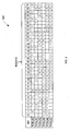
- Fig. 2 is a table illustrating a modified Hamming code used to generate check bits in response to a data word, in accordance with one embodiment of the present invention.
- Fig. 3 is a circuit diagram of partial syndrome decoder in accordance with one embodiment of the present invention.
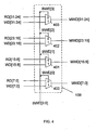
- Fig. 4 is a block diagram of a multiplexer circuit used in accordance with one embodiment of the present invention.
- Fig. 1 is a block diagram of a memory system 100, which implements a partial-word write with predictive error correction in accordance with one embodiment of the present invention.
- Memory system 100 includes memory array 101, error correction code (ECC) generators 102-103, exclusive OR circuits 104-106, syndrome decoder 107, partial syndrome decoder 108, multiplexer circuit 109 and logical AND circuit 110.
- ECC error correction code
- memory array 101 is organized as 32k words of 32-bits each, and uses 6 check bits to facilitate single-bit error correction.
- other word sizes and check bit widths can be used in other embodiments.
- memory system 100 supports byte-write transactions using a read-modify-write operation.
- Memory system 100 provides a standard interface similar to interfaces used in common synchronous SRAM systems.
- memory array 101 operates in response to an address signal A[14:0], a chip enable signal CE, a read/write indicator signal RW# and a clock signal CLK.
- Memory array 101 includes conventional circuitry, such as sense-amplifiers, and address decoders, associated with a semiconductor memory.
- a read data word RD[31:0] and corresponding check bits RCB 0 [5:0] are read from memory 101.
- the read data word RD[31:0] is provided to ECC generator 102, exclusive OR circuit 105 and multiplexer 109.
- the read check bits RCB 0 [5:0] are provided to exclusive OR circuit 104.
- ECC generator 102 generates a set of read check bits RCB 1 [5:0] in response to the read data word RD[31:0]. These read check bits RCB 1 ⁇ 5:0] are also provided to exclusive OR circuit 104.
- Exclusive OR circuit 304 generates a syndrome word SYN[5:0] in response to the read check bits RCB 0 [5:0] and RCB 1 [5:0].
- This syndrome word SYN[5:0] is applied to syndrome decoder 107, partial syndrome decoder 108 and logical AND circuit 110.
- Syndrome decoder 107 generates a read error correction code RECC[31:0] in response to the syndrome word SYN[5:0].
- This read error correction code RECC[31:0] is provided to exclusive OR circuit 105.
- Exclusive OR circuit 105 provides a read output word Q[31:0] in response to the read data word RD[31:0] and read error correction code RECC[31:0].
- Byte write enable signals BWE[3:0] are provided to partial syndrome decoder 108 and to the control terminals of multiplexer circuit 109.
- Partial syndrome decoder 108 provides a write check bit correct signal WCBCOR to logical AND circuit 110 in response to the syndrome word SYN[5:0] and the byte write enable signals BWE[3:0].
- Logical AND circuit 110 provides write check bits WCB 1 [5:0] to exclusive OR circuit 106 in response to the syndrome word SYN[5:0] and write check bit correct signal WCBCOR.
- Multiplexer 109 also receives a write data word WD[31:0].
- This multiplexer 109 provides a merged write data word MWD[31:0] in response to the byte write enable signals BWE[3:0], the read data word RD[31:0] and the write data word WD[31:0].
- the merged write data word MWD[31:0] is provided to memory array 101 and ECC generator 103.
- ECC generator 103 generates write check bits WCB 0 [5:0] in response to the merged write data word MWD[31:0].
- Exclusive OR circuit 106 provides write check bits WCB 2 [3:0] to memory array 101 in response to write check bits WCB 1 [5:0] and WCB 0 [3:0].
- the read-modify-write operation has an associated write address A[14:0], which identifies the word location to be written.
- the read-modify-write operation also has associated byte write enable signals BWE[3:0], which indicate which of the four bytes in the addressed word location are to be written.
- byte write enable signals BWE[3:0] having values of "0011" would indicate that the first and second bytes of the addressed word will be written, while the third and fourth bytes of the addressed word will not be written.
- the byte write enable signals BWE[3:0] allow any combination of the 4 bytes in a word to be written in one write transaction.
- a read operation is performed to the specified write address in memory array 101, thereby causing a 4-byte read data word RD[31:0] and associated read check bits RCB 0 [5:0] to be read from memory array 101.
- FIG. 2 is a table 200 illustrating the modified Hamming code used to generate read check bits RCB 1 [5:0] in response to the read data word RD[31:0], in accordance with one embodiment of the present example.
- the read check bits RCB 0 [5:0] were originally generated using the same modified Hamming code illustrated in table 200.
- Columns 0 to 63 of table 200 show the ECC code for the corresponding bits of the read data word RD[31:0].
- Rows 0 to 5 shows the parity generation of the corresponding read check bits RCB 1 [5:0].
- read check bit RCB 1 [3] is generated by performing an exclusive OR operation on the indicated bits RD[0:23] of read data word RD[31:0]. If an odd number of the indicated bits have a logic "1" value, then read check bit RCB 1 [3] will have a logic "1” value. Conversely if an even number of the indicated bits have a logic "1” value, then read check bit RCB 1 [3] will have a logic "0" value. Read check bits RCB 1 [0:2] and RCB 1 [4:5] are generated in a similar manner in response to the indicated bits.
- ECC generator 102 incorporates 3-levels of exclusive OR logic gates.
- the exclusive-OR tree implementation of modified Hamming code is well understood in the field of error correction codes and therefore is not further elaborated. The described modified Hamming code allows for single-bit error correction.
- Read check bit values RCB 0 [5:0] and RCB 1 [5:0] are provided to exclusive OR circuit 104.
- exclusive OR circuit 104 performs a bit-wise comparison of the two read check bit values RCB 0 [5:0] and RCB 1 [5:0] using six 2-input exclusive OR gates. For example, if read check bit RCB 0 [0] matches read check bit RCB 1 [0], then exclusive OR circuit 104 will provide a corresponding syndrome bit SYN[0] having a logic "0" value. Thus, as long as the read check bits RCB 0 [5:0] match the read check bits RCB 1 [5:0], the syndrome word SYN[5:0] will have all logic "0" values (i.e., "000000”)
- exclusive OR circuit 104 will provide a corresponding syndrome bit SYN[0] having a logic "1" value.
- the syndrome bits SYN[5:3] will have a value of "011".
- the syndrome bits SYN[5:3] will have a value of "111". If a single-bit error exists in the read data bits RD[23:16] (i.e., byte[2]) of the read data word RD[31:0], then the syndrome bits SYN[5:3] will have a value of "101".
- the syndrome bits SYN[2:0] have a value that identifies the location of the error bit within the read data word identified by the syndrome bits SYN[5:3]. For example, if syndrome bits SYN[5:3] have a value of "111" and syndrome bits SYN[2:0] have a value of "010", a single bit error exists in read data bit RD[10] (i.e., bit location [2] of byte[1]). In this manner, exclusive OR circuit 104 provides the syndrome word SYN[5:0].
- Syndrome decoder 107 decodes the syndrome word SYN[5:0], thereby providing read error correction code RECC[31:0].
- syndrome decoder 107 is a 6-to-32 decoder implemented using two levels of AND gates. This type of implementation using combinatorial logic is well known in the art of logic design and therefore is not described further. If there is a single-bit error associated with the read data word RD[31:0], the read error correction code RECC[31:0] provided by the 32-bit syndrome decoder 107 will exhibit a logic '1' bit that identifies the location of the single-bit error in read data value RD[31:0].
- both the syndrome word SYN[5:0] and the read error correction code RECC[31:0] will have all logic "0" bits.
- the read data value RD[31:0] and the read error correction code RECC[31:0] are applied to exclusive OR circuit 105, thereby creating corrected read data value Q[31:0].
- Partial syndrome decoder 108 also receives the syndrome word SYN[5:0] and the byte write enable signals BWE[3:0].
- Fig. 3 is a circuit diagram of partial syndrome decoder 108 in accordance with one embodiment of the present invention. As described in more detail below, partial syndrome decoder 108 determines whether a single-bit error exists in a byte that is not being overwritten with new data, as identified by the byte write enable signals BWE[3:0]. Partial syndrome decoder 108 includes logic NAND gates 301-305, which are connected as illustrated.
- Logic NAND gate 301 receives syndrome bits SYN[5:3] and byte write enable signal BWE[0], wherein syndrome bit SYN[5] and byte write enable signal BWE[0] are provided on inverting input terminals. If the syndrome bits SYN[5:3] have a value of "011" (indicating that a single bit error exists in read data byte RD[7:0] of read data word RD[31:0]) and the byte write enable signal BWE[0] has a logic "0" value (indicating that read data byte RD[7:0] is not being written in the present write operation), then NAND gate 301 provides a logic "0" output signal. Otherwise, NAND gate 301 provides a logic "1" output signal.
- Logic NAND gate 302 receives syndrome bits SYN[5:3] and byte write enable signal BWE[1], wherein byte write enable signal BWE[1] is provided on an inverting input terminal. If the syndrome bits SYN[5:3] have a value of "111" (indicating that a single-bit error exists in read data byte RD[15:8]) and the byte write enable signal BWE[1] has a logic "0" value (indicating that read data byte RD[15:8] is not being written in the present write operation), then NAND gate 302 provides a logic "0" output signal. Otherwise, NAND gate 302 provides a logic "1" output signal.
- Logic NAND gate 303 receives syndrome bits SYN[5:3] and byte write enable signal BWE[2], wherein syndrome bit SYN[4] and byte write enable signal BWE[2] are provided on inverting input terminals. If the syndrome bits SYN[5:3] have a value of "101" (indicating that a single bit error exists in read data byte RD[23:16]) and the byte write enable signal BWE[2] has a logic "0" value (indicating that read data byte RD[23:16] is not being written in the present write operation), then NAND gate 303 provides a logic "0" output signal. Otherwise, NAND gate 303 provides a logic "1" output signal.
- Logic NAND gate 304 receives syndrome bits SYN[5:3] and byte write enable signal BWE[3], wherein syndrome bit SYN[3] and byte write enable signal BWE[3] are provided on inverting input terminals. If the syndrome bits SYN[5:3] have a value of "110" (indicating that a single bit error exists in read data byte RD[31:24]) and the byte write enable signal BWE[3] has a logic "0" value (indicating that read data byte RD[31:24] is not being written in the present write operation), then NAND gate 304 provides a logic "0" output signal. Otherwise, NAND gate 304 provides a logic "1" output signal.
- NAND gate 305 will provide a logic "1" write check bit correction (WCBCOR) signal.
- WCBCOR write check bit correction
- the WCBCOR signal is provided to AND circuit 110, along with syndrome word SYN[5:0]. Within AND circuit 110, each bit of the syndrome word SYN[5:0] is logically ANDed with the WCBCOR signal, thereby providing write check bits WCB 1 [5:0]. If the WCBCOR signal has a logic "0" value, then all of the write check bits WCB 1 [5:0] have a logic "0" value. If the WCBCOR signal has a logic "1" value, then the syndrome word SYN[5:0] is effectively routed as the write check bits WCB 1 [5:0]. The functionality of the write check bits WCB 1 [5:0] is described in more detail below.
- the read data word RD[31:0] and the partial-word write data in write data value WD[31:0] are applied to multiplexer 109.
- the byte write enable signals BWE[3:0], which identify which of the four bytes in the read data word RD[31:0] are being replaced by bytes in the write data word WD[31:0], are applied to the control terminals of multiplexer 109.
- Fig. 4 is a block diagram of multiplexer circuit 109 in accordance with one embodiment of the present invention.
- Multiplexer circuit 109 includes multiplexers 400, 401, 402 and 403, which are controlled by the byte write enable signals BWE[0] , BWE[1] , BWE[2] and BWE[3], respectively.
- Multiplexer 400 is configured to receive bytes RD[7:0] and WD[7:0] and provide merged write byte MWD[7:0].
- Multiplexer 401 is configured to receive bytes RD[15:8] and WD[15:8] and provide merged write byte MWD[15:8].
- Multiplexer 402 is configured to receive bytes RD[23:16] and WD[23:16] and provide merged write byte MWD[23:16].
- Multiplexer 403 is configured to receive bytes RD[31:24] and WD[31:24] and provide merged write byte MWD[31:24].
- a byte write enable signal BWE[n] has a logic "1" value
- the associated write data byte WD is routed by multiplexer circuit 109.
- a byte write enable signal BWE[n] has a logic "0” value
- the associated read data byte RD is routed by multiplexer circuit 109.
- byte write enable signals BWE[3:0] having values of "0011” would cause multiplexer circuit 109 to route the read data bytes RD[31:24] and RD [23:16] and the write data bytes WD[15:8] and WD[7:0], to create the merged write data value WMD[31:0].
- the merged write data value MWD[31:0] is provided to ECC generator 103.
- ECC generator 103 generates a set of write check bits WCB 0 [5:0] associated with the merged write data value MWD[31:0].
- ECC generator 103 uses the same modified Hamming code as ECC generator 102.
- the new write check bits WCB 0 [5:0] are provided to exclusive OR circuit 106, along with write check bits WCB 1 [5:0].
- Exclusive OR circuit 304 generates write check bits WEB 2 [5:0] in response to the write check bits WCB 0 [5:0] and WCB 1 [5:0].
- partial syndrome decoder 108 determines that there is no error in read data word RD[31:0], or that a single-bit error exists in a byte of the read data word RD[31:0] that is being overwritten by a byte of the write data word WD[31:0], the write check bits WCB 1 [5:0] will have all logic "0" values. In this case, the write check bits WCB 0 [5:0] are routed through exclusive OR circuit 106 without modification as the write check bits WCB 2 [5:0] .
- partial syndrome decoder 108 determines that there is a single-bit error in a byte of the read data word RD[31:0] that is not being overwritten by a byte of the write data word WD[31:0]
- the write check bits WCB 1 [5:0] will have a value equal to the syndrome word SYN[5:0].
- the write check bits WCB 1 [5:0] will cause exclusive OR circuit 106 to modify the write check bits WCB 0 [5:0] to create the write check bits WCB 2 ⁇ 5:0]. The significance of this modification is described in more detail below.
- the merged write data MWD[31:0] and the write check bits WCB 2 [5:0] are written to memory array 101.
- ECC generator 102, exclusive OR circuit 104 and partial syndrome decoder 108 and logic AND circuit 110 operate in parallel with multiplexer circuit 109 and ECC generator 103. That is, read check bit generation, syndrome generation and partial syndrome decoding is executed in parallel with data merging and write check bit generation.
- the write check bits WCB 0 [31:0] are generated in response to the uncorrected read data word RD[31:0].
- the write check bits WCB 0 [31:0] may contain incorrect values if an uncorrected error in the read data word RD[31:0] is actually used to generate the write check bits WCB 0 [31:0].
- this situation is indicated when the WCBCOR signal has a logic "1" value.
- the write check bits WCB 0 [5:0] are corrected when exclusive OR'ed with write check bits WCB 1 [5:0].
- syndrome word SYN[5:0] is governed by the column (bit) location of the error bit in the parity-check matrix of Fig. 2 . For example, if read data bit RD[12] has an error, the syndrome word SYN[5:0] will have a value of "111100".
- the write check bits WCB 0 [5:0] generated in response to the merged write data word MWD[31:0] are incorrect.
- the correct write check bits WCB 2 [5:0] and the incorrect write check bits WCB 0 [5:0] differ by a value equal to the write check bits WCB 1 [5:0]. Therefore, the correct write check bits WCB 2 [5:0] can be obtained by performing a bit-wise exclusive OR operation on write check bits WCB 0 [5:0] and WCB 1 [5:0]. In this manner, write check bits WCB 2 [31:0] are generated in a predictive manner.
- the present invention ensures that the write check bits are generated correctly even if the data bits in the merged write data word contain a single-bit error. In doing so, the present invention ensures that the single-bit error can be corrected if the data is read in a subsequent read transaction.
- the total partial-word write time of the present embodiment thus consists of: (1) a memory read operation, (2) read check bit generation, (3) syndrome generation, (4) partial syndrome decode, (5) write check bit correction, and (6) data write to memory. Note that the steps of data merging and write check bit generation are done in parallel with read check bit generation and syndrome generation.
- Typical timing for transactions (1)-(6) in a memory having a capacity of 1M bits, a 38-bit ECC word and fabricated with a 0.13um CMOS technology are: 1.5 ns, 1 ns, 0.1 ns, 0.1 ns, and 1.5 ns, respectively.
- the read-modify-write operation of the present invention therefore takes about 4.2 ns.
- the predictive ECC generation in the read-modify-write process works correctly only if the ECC word, consisting of the read data word RD[31:0] and read check bits RCB 0 [5:0], has no more than 1 error bit. In general, this assumption is satisfied in an ECC that can only detect and correct for 1 error bit.
- bits in any ECC word read from any memory location have random states. That is, the check bits and data bits have no relationship. Therefore, multiple bit errors may occur and the ECC detection and correction logic cannot handle this multiple-bit error correctly. As a result, the merged data word contains random data bits and the write check bits are not generated correctly.
- the memory location to which MWD[31:0] and WCB 2 [5:0] are written will contain a ECC word which will contain one or zero error bits, assuming that the memory array 101 does not have more than one defective bit at the memory location.
- the memory can be initialized by performing 32-bit word write to all memory locations with a fixed data word, for example 00000000H, during system initialization or by performing a Built-In-Self-Test (BIST) operation before any read or write access.
- the initialization can be carried out one memory location at a time during normal system operation by making sure that the first write to any memory location is a 32-bit word write with all the byte-write enable bits in BWE[3:0] in the high state.
- Another alternative is to implement a memory clear function, which sets the content of every memory cell to zero state, such that the data word and ECC bits are consistent in every memory location.
- the clear function can be activated by a memory reset signal.
Landscapes
- Engineering & Computer Science (AREA)
- Theoretical Computer Science (AREA)
- Quality & Reliability (AREA)
- Physics & Mathematics (AREA)
- General Engineering & Computer Science (AREA)
- General Physics & Mathematics (AREA)
- Computer Security & Cryptography (AREA)
- Microelectronics & Electronic Packaging (AREA)
- Computer Hardware Design (AREA)
- Techniques For Improving Reliability Of Storages (AREA)
- Detection And Correction Of Errors (AREA)
- Dram (AREA)
Claims (15)
- Verfahren zum Ausführen einer Teilwort-Schreibtransaktion in einem Speichersystem, das Fehlercode-Korrektur durchführt, wobei das Verfahren Folgendes beinhaltet:Lesen eines ersten Datenwortes mit mehreren Teilwörtern und einem Satz Lese-Check-Bits aus einer Adresse eines Speichers;Ermitteln, dass ein Fehler im ersten Datenwort vorliegt, und Erkennen eines gelesenen Datenteilwortes des ersten Datenwortes, das den Fehler enthält;Vereinigen eines oder mehrerer Teilwörter des ersten Datenwortes mit einem oder mehreren Teilwörtern eines Schreibdatenwortes, um ein vereinigtes Datenwort zu schaffen, wobei das vereinigte Datenwort den Fehler enthält;Erzeugen eines Satzes von Schreib-Check-Bits als Reaktion auf das vereinigte Datenwort;Modifizieren des Satzes von Schreib-Check-Bits als Reaktion auf das erste Datenwort und den Satz von Lese-Check-Bits, um dadurch einen modifizierten Satz von Schreib-Check-Bits zu erzeugen;Schreiben des modifizierten Satzes von Schreib-Check-Bits auf die Adresse des Speichers; und gekennzeichnet durch:Schreiben des vereinigten Datenwortes auf die Adresse des Speichers.
- Verfahren nach Anspruch 1, wobei der Schritt des Ermittelns, dass ein Fehler im ersten Datenwort vorliegt, parallel zu den Schritten des Vereinigens eines oder mehrerer Teilwörter des ersten Datenwortes mit einem oder mehreren Teilwörtern eines Schreibdatenwortes und des Erzeugens eines Satzes von Schreib-Check-Bits als Reaktion auf das vereinigte Datenwort ausgeführt wird.
- Verfahren nach Anspruch 1, wobei der Schritt des Ermittelns, dass ein Fehler im ersten Datenwort vorliegt, Folgendes beinhaltet:Erzeugen eines zweiten Satzes von Lese-Check-Bits als Reaktion auf die mehreren Teilwörter des ersten Datenwortes; undErzeugen eines Syndromwortes als Reaktion auf den Satz von Lese-Check-Bits des ersten Datenwortes und des zweiten Satzes von Lese-Check-Bits, wobei das Syndromwort einen Ort des Fehlers in den Teilwörtern des ersten Datenwortes erkennt.
- Verfahren nach Anspruch 3, wobei der Schritt des Modifizierens des Satzes von Schreib-Check-Bits das Modifizieren der Schreib-Check-Bits als Reaktion auf das Syndromwort beinhaltet.
- Verfahren nach Anspruch 4, wobei der Schritt des Modifizierens des Satzes von Schreib-Check-Bits das Kombinieren der Schreib-Check-Bits mit dem Syndromwort mittels einer Exklusiv-ODER-Funktion beinhaltet.
- Verfahren nach Anspruch 3, das ferner das Ermitteln beinhaltet, dass das Lesedaten-Teilwort des ersten Datenwortes, das den Fehler enthält, in dem vereinigten Datenwort enthalten ist, als Reaktion auf ein Teilwort-Write-Enable-Signal, das die Teilwörter des in dem vereinigten Datenwort enthaltenen Schreibdatenwortes erkennt.
- Verfahren nach Anspruch 3, wobei die Schritte des Erzeugens des zweiten Satzes von Lese-Check-Bits und des Erzeugens des Syndromwortes parallel zu den Schritten des Vereinigens eines oder mehrerer Teilwörter des Lesedatenwortes mit einem oder mehreren Teilwörtern des Schreibdatenwortes und des Erzeugens des Satzes von Schreib-Check-Bits ausgeführt werden.
- Verfahren nach Anspruch 1, das ferner Folgendes beinhaltet:Lesen eines zweiten Datenwortes mit mehreren Teilwörtern und einem zweiten Satz von Lese-Check-Bits aus einer Adresse eines Speichers;Ermitteln, dass kein Fehler im zweiten Datenwort vorliegt;Vereinigen eines oder mehrerer Teilwörter des zweiten Datenwortes mit einem oder mehreren Teilwörtern eines zweiten Schreibdatenwortes, um dadurch ein zweites vereinigtes Datenwort zu schaffen;Erzeugen eines zweiten Satzes von Schreib-Check-Bits als Reaktion auf das zweite vereinigte Datenwort; undSchreiben des zweiten vereinigten Datenwortes und des zweiten Satzes von Schreib-Check-Bits auf die Adresse des Speichers.
- Speichersystem, das Folgendes umfasst:einen Speicher (101), der ein erstes Datenwort mit mehreren Teilwörtern und einem ersten Satz von Lese-Check-Bits auf einer Adresse speichert;Mittel (102, 106) zum Ermitteln, dass ein Fehler in den Teilwörtern des ersten Datenwortes vorliegt, und zum Erkennen eines Lesedaten-Teilwortes des ersten Datenwortes, das den Fehler enthält;Mittel zum Vereinigen (109) eines oder mehrerer Teilwörter des ersten Datenwortes mit einem oder mehreren Teilwörtern eines Schreibdatenwortes, um dadurch ein vereinigtes Datenwort zu schaffen;Mittel (108) zum Ermitteln, dass das vereinigte Datenwort den Fehler enthält;Mittel (103) zum Erzeugen eines Satzes von Schreib-Check-Bits als Reaktion auf das vereinigte Datenwort;Mittel (110, 106) zum Modifizieren des Satzes von Schreib-Check-Bits als Reaktion auf das erste Datenwort und den Satz von Lese-Check-Bits, um einen modifizierten Satz von Schreib-Check-Bits zu schaffen, die den Fehler erkennen;und Mittel zum Schreiben des modifizierten Satzes von Schreib-Check-Bits auf die Adresse des Speichers, und gekennzeichnet durch Mittel zum Schreiben des vereinigten Datenwortes auf die Adresse des Speichers.
- Speichersystem nach Anspruch 9, wobei Mittel zum Ermitteln, dass ein Fehler in den Teilwörtern des ersten Datenwortes vorliegt, Folgendes umfassen:einen ersten Fehlerkorrekturcode-(ECC)-Generator (102), der einen zweiten Satz von Lese-Check-Bits als Reaktion auf die Teilwörter des ersten Datenwortes erzeugt; undein Logikgatter (104), das ein Syndromwort als Reaktion auf den ersten Satz von Lese-Check-Bits und den zweiten Satz von Lese-Check-Bits erzeugt.
- Speichersystem nach Anspruch 10, wobei das Mittel zum Vereinigen einen Multiplexer (109) umfasst, der die Teilwörter des ersten Datenwortes, die Teilwörter des Schreibdatenwortes und ein Teilwort-Write-Enable-Signal empfängt, das ein oder mehrere in das vereinigte Datenwort einzuschließende Teilwörter des Schreibdatenwortes identifiziert.
- Speichersystem nach Anspruch 11, wobei das Mittel zum Ermitteln, dass das vereinigte Datenwort den Fehler enthält, einen Teilsyndromgenerator (108) umfasst, der so geschaltet ist, dass er das Syndromwort und das Teilwort-Write-Enable-Signal empfängt, wobei der Teilsyndromgenerator (108) ein Korrektursteuersignal erzeugt, das anzeigt, ob das vereinigte Datenwort den Fehler enthält.
- Speichersystem nach Anspruch 10, wobei das Mittel zum Erzeugen eines Satzes von Schreib-Check-Bits als Reaktion auf das vereinigte Datenwort einen zweiten ECC-Generator (103) umfasst, wobei der erste ECC-Generator und der zweite ECC-Generator dieselbe Fehlerkorrekturcode-Funktion implementieren.
- Speichersystem nach Anspruch 10, wobei das Mittel zum Modifizieren des Satzes von Schreib-Check-Bits eine Logikschaltung (106) umfasst, die den Satz von Schreib-Check-Bits mit dem Syndromwort kombiniert, um den modifizierten Satz von Schreib-Check-Bits zu erzeugen.
- Speichersystem nach Anspruch 9, wobei das Mittel zum Ermitten, dass ein Fehler in den Teilwörtern des ersten Datenwortes vorliegt, und das Mittel zum Ermitteln, dass das vereinigte Datenwort den Fehler enthält, sich in einem ersten Pfad des Speichersystems befinden, und wobei das Mittel zum Vereinigen und das Mittel zum Erzeugen eines Satzes von Schreib-Check-Bits als Reaktion auf das vereinigte Datenwort sich in einem zweiten Pfad des Speichersystems befinden, wobei der erste Pfad des Speichersystems parallel zum zweiten Pfad des Speichersystems wirkt.
Applications Claiming Priority (2)
| Application Number | Priority Date | Filing Date | Title |
|---|---|---|---|
| US10/997,604 US7392456B2 (en) | 2004-11-23 | 2004-11-23 | Predictive error correction code generation facilitating high-speed byte-write in a semiconductor memory |
| PCT/US2005/040086 WO2006057793A2 (en) | 2004-11-23 | 2005-11-03 | Predictive error correction code generation facilitating high-speed byte-write in a semiconductor memory |
Publications (3)
| Publication Number | Publication Date |
|---|---|
| EP1815338A2 EP1815338A2 (de) | 2007-08-08 |
| EP1815338A4 EP1815338A4 (de) | 2008-05-28 |
| EP1815338B1 true EP1815338B1 (de) | 2010-08-11 |
Family
ID=36462279
Family Applications (1)
| Application Number | Title | Priority Date | Filing Date |
|---|---|---|---|
| EP05823321A Expired - Lifetime EP1815338B1 (de) | 2004-11-23 | 2005-11-03 | Prädiktive generierung von fehlerkorrekturkodes für hochgeschwindigkeits-byte-schreiben in einem halbleiterspeicher |
Country Status (5)
| Country | Link |
|---|---|
| US (2) | US7392456B2 (de) |
| EP (1) | EP1815338B1 (de) |
| AT (2) | ATE477537T1 (de) |
| DE (1) | DE602005022916D1 (de) |
| WO (1) | WO2006057793A2 (de) |
Families Citing this family (48)
| Publication number | Priority date | Publication date | Assignee | Title |
|---|---|---|---|---|
| JP2006309147A (ja) * | 2005-03-30 | 2006-11-09 | Kyocera Mita Corp | トナーカートリッジ及びそのシャッタ構造 |
| US7274618B2 (en) * | 2005-06-24 | 2007-09-25 | Monolithic System Technology, Inc. | Word line driver for DRAM embedded in a logic process |
| US7499307B2 (en) * | 2005-06-24 | 2009-03-03 | Mosys, Inc. | Scalable embedded DRAM array |
| EP1748374A1 (de) * | 2005-07-08 | 2007-01-31 | STMicroelectronics SA | Verfahren und Vorrichtung zum Schutz eines Speichers gegen Angriffe mittels Fehlerinjektion |
| EP1980946B1 (de) * | 2006-01-31 | 2013-05-29 | Fujitsu Limited | Verfahren zur erzeugung eines fehlerkorrekturcodes und speicherverwaltungseinrichtung |
| JP2007242162A (ja) * | 2006-03-09 | 2007-09-20 | Toshiba Corp | 半導体記憶装置 |
| US8069377B2 (en) * | 2006-06-26 | 2011-11-29 | Micron Technology, Inc. | Integrated circuit having memory array including ECC and column redundancy and method of operating the same |
| US7844888B2 (en) * | 2006-09-29 | 2010-11-30 | Qimonda Ag | Electronic device, method for operating an electronic device, memory circuit and method of operating a memory circuit |
| US8042022B2 (en) * | 2007-03-08 | 2011-10-18 | Micron Technology, Inc. | Method, system, and apparatus for distributed decoding during prolonged refresh |
| US8156402B2 (en) * | 2007-04-26 | 2012-04-10 | Agere Systems Inc. | Memory device with error correction capability and efficient partial word write operation |
| US7930615B2 (en) | 2007-05-31 | 2011-04-19 | Agere Systems Inc. | Memory device with error correction capability and preemptive partial word write operation |
| JP4764945B2 (ja) * | 2007-06-20 | 2011-09-07 | 富士通株式会社 | キャッシュ制御装置、キャッシュ制御方法およびキャッシュ制御プログラム |
| US20090070655A1 (en) * | 2007-09-11 | 2009-03-12 | Silicon Motion, Inc. | Method for Generating an ECC Code for a Memory Device |
| JP4820795B2 (ja) * | 2007-10-04 | 2011-11-24 | パナソニック株式会社 | 半導体記憶装置 |
| US8452920B1 (en) * | 2007-12-31 | 2013-05-28 | Synopsys Inc. | System and method for controlling a dynamic random access memory |
| US7814300B2 (en) | 2008-04-30 | 2010-10-12 | Freescale Semiconductor, Inc. | Configurable pipeline to process an operation at alternate pipeline stages depending on ECC/parity protection mode of memory access |
| US20090327535A1 (en) * | 2008-06-30 | 2009-12-31 | Liu Tz-Yi | Adjustable read latency for memory device in page-mode access |
| US8161355B2 (en) | 2009-02-11 | 2012-04-17 | Mosys, Inc. | Automatic refresh for improving data retention and endurance characteristics of an embedded non-volatile memory in a standard CMOS logic process |
| JP2013033560A (ja) | 2009-12-03 | 2013-02-14 | Panasonic Corp | 半導体記憶装置 |
| KR20110087036A (ko) * | 2010-01-25 | 2011-08-02 | 삼성전자주식회사 | 덮어쓰기 가능한 불휘발성 메모리 장치 및 그것의 데이터 쓰기 방법 |
| US8438344B2 (en) * | 2010-03-12 | 2013-05-07 | Texas Instruments Incorporated | Low overhead and timing improved architecture for performing error checking and correction for memories and buses in system-on-chips, and other circuits, systems and processes |
| US8621324B2 (en) | 2010-12-10 | 2013-12-31 | Qualcomm Incorporated | Embedded DRAM having low power self-correction capability |
| US8612834B2 (en) * | 2011-03-08 | 2013-12-17 | Intel Corporation | Apparatus, system, and method for decoding linear block codes in a memory controller |
| KR101788737B1 (ko) * | 2011-05-12 | 2017-10-24 | 에스케이하이닉스 주식회사 | 반도체 시스템 |
| US9003260B2 (en) * | 2011-06-29 | 2015-04-07 | Texas Instruments Incorporated | Partial-writes to ECC (error check code) enabled memories |
| US8707133B2 (en) | 2011-12-05 | 2014-04-22 | Lsi Corporation | Method and apparatus to reduce a quantity of error detection/correction bits in memory coupled to a data-protected processor port |
| US8869008B2 (en) | 2013-01-17 | 2014-10-21 | Apple Inc. | Adaptation of analog memory cell read thresholds using partial ECC syndromes |
| CN105340022B (zh) * | 2013-06-24 | 2019-11-12 | 美光科技公司 | 用于校正数据错误的电路、设备及方法 |
| GB2516831B (en) | 2013-07-31 | 2020-10-21 | Advanced Risc Mach Ltd | Error code management in systems permitting partial writes |
| CN110265071B (zh) | 2013-09-24 | 2023-05-12 | 拉姆伯斯公司 | 具有内部读取-修改-写入操作的存储部件 |
| US9495242B2 (en) | 2014-07-30 | 2016-11-15 | International Business Machines Corporation | Adaptive error correction in a memory system |
| US9583219B2 (en) | 2014-09-27 | 2017-02-28 | Qualcomm Incorporated | Method and apparatus for in-system repair of memory in burst refresh |
| US10298271B2 (en) | 2015-02-03 | 2019-05-21 | Infineon Technologies Ag | Method and apparatus for providing a joint error correction code for a combined data frame comprising first data of a first data channel and second data of a second data channel and sensor system |
| US10289508B2 (en) | 2015-02-03 | 2019-05-14 | Infineon Technologies Ag | Sensor system and method for identifying faults related to a substrate |
| US9412461B1 (en) * | 2015-03-10 | 2016-08-09 | Kabushiki Kaisha Toshiba | Nonvolatile semiconductor memory device |
| US10346170B2 (en) * | 2015-05-05 | 2019-07-09 | Intel Corporation | Performing partial register write operations in a processor |
| US20160378151A1 (en) * | 2015-06-26 | 2016-12-29 | Intel Corporation | Rack scale architecture (rsa) and shared memory controller (smc) techniques of fast zeroing |
| US10522237B2 (en) | 2015-08-07 | 2019-12-31 | Mentor Graphics Corporation | Low power VLSI designs using circuit failure in sequential cells as low voltage check for limit of operation |
| US10025652B2 (en) | 2015-10-27 | 2018-07-17 | Western Digital Technologies, Inc. | Error location pointers for non volatile memory |
| US9904595B1 (en) * | 2016-08-23 | 2018-02-27 | Texas Instruments Incorporated | Error correction hardware with fault detection |
| US10372531B2 (en) * | 2017-01-05 | 2019-08-06 | Texas Instruments Incorporated | Error-correcting code memory |
| KR20190031787A (ko) | 2017-09-18 | 2019-03-27 | 삼성전자주식회사 | 병렬 리드-모디파이-라이트 동작을 수행하는 메모리 장치 |
| US10691532B2 (en) | 2018-06-29 | 2020-06-23 | Alibaba Group Holding Limited | Storage drive error-correcting code-assisted scrubbing for dynamic random-access memory retention time handling |
| US11042181B2 (en) * | 2018-11-01 | 2021-06-22 | Siemens Industry Software Inc. | Local clock injection and independent capture for circuit test of multiple cores in clock mesh architecture |
| JP7177948B2 (ja) * | 2019-10-15 | 2022-11-24 | 株式会社ソニー・インタラクティブエンタテインメント | 情報処理装置、及び情報処理方法 |
| US11398289B2 (en) * | 2020-01-27 | 2022-07-26 | Stmicroelectronics International N.V. | Memory calibration device, system and method |
| US11094372B1 (en) * | 2020-05-07 | 2021-08-17 | Powerchip Semiconductor Manufacturing Corporation | Partial writing method of dram memoryl device to reduce power consumption associated with large voltage swing of internal input/output lines |
| US11847348B2 (en) * | 2021-08-24 | 2023-12-19 | Apple Inc. | Multi-activation techniques for partial write operations |
Family Cites Families (85)
| Publication number | Priority date | Publication date | Assignee | Title |
|---|---|---|---|---|
| US3814921A (en) * | 1972-11-15 | 1974-06-04 | Honeywell Inf Systems | Apparatus and method for a memory partial-write of error correcting encoded data |
| US3969706A (en) * | 1974-10-08 | 1976-07-13 | Mostek Corporation | Dynamic random access memory misfet integrated circuit |
| US4045783A (en) * | 1976-04-12 | 1977-08-30 | Standard Microsystems Corporation | Mos one transistor cell ram having divided and balanced bit lines, coupled by regenerative flip-flop sense amplifiers, and balanced access circuitry |
| JPS5555499A (en) | 1978-10-16 | 1980-04-23 | Nec Corp | Memory control unit |
| JPS5647988A (en) * | 1979-09-20 | 1981-04-30 | Nec Corp | Semiconductor memory device |
| US4317201A (en) * | 1980-04-01 | 1982-02-23 | Honeywell, Inc. | Error detecting and correcting RAM assembly |
| US4380812A (en) * | 1980-04-25 | 1983-04-19 | Data General Corporation | Refresh and error detection and correction technique for a data processing system |
| US4345328A (en) * | 1980-06-30 | 1982-08-17 | Sperry Corporation | ECC Check bit generation using through checking parity bits |
| US5177743A (en) * | 1982-02-15 | 1993-01-05 | Hitachi, Ltd. | Semiconductor memory |
| US4561095A (en) * | 1982-07-19 | 1985-12-24 | Fairchild Camera & Instrument Corporation | High-speed error correcting random access memory system |
| JPS60219700A (ja) * | 1984-04-13 | 1985-11-02 | Sharp Corp | 誤り訂正機能内蔵半導体集積回路 |
| JPS6134793A (ja) * | 1984-07-27 | 1986-02-19 | Hitachi Ltd | ダイナミツクメモリ装置における診断及びエラ−訂正装置 |
| US4726021A (en) * | 1985-04-17 | 1988-02-16 | Hitachi, Ltd. | Semiconductor memory having error correcting means |
| US4933904A (en) * | 1985-11-29 | 1990-06-12 | General Electric Company | Dense EPROM having serially coupled floating gate transistors |
| US4794597A (en) * | 1986-03-28 | 1988-12-27 | Mitsubishi Denki Kabushiki Kaisha | Memory device equipped with a RAS circuit |
| US4768197A (en) * | 1986-09-15 | 1988-08-30 | Amdahl Corporation | Cache error code update |
| JPH07118193B2 (ja) * | 1986-09-18 | 1995-12-18 | 富士通株式会社 | 半導体記憶装置 |
| US4740968A (en) * | 1986-10-27 | 1988-04-26 | International Business Machines Corporation | ECC circuit failure detector/quick word verifier |
| US4939694A (en) * | 1986-11-03 | 1990-07-03 | Hewlett-Packard Company | Defect tolerant self-testing self-repairing memory system |
| US4817095A (en) * | 1987-05-15 | 1989-03-28 | Digital Equipment Corporation | Byte write error code method and apparatus |
| US4782487A (en) * | 1987-05-15 | 1988-11-01 | Digital Equipment Corporation | Memory test method and apparatus |
| US4884271A (en) * | 1987-12-28 | 1989-11-28 | International Business Machines Corporation | Error checking and correcting for read-modified-write operations |
| JPH01183000A (ja) * | 1988-01-14 | 1989-07-20 | Mitsubishi Electric Corp | 誤り訂正回路を有する半導体メモリ装置 |
| US5008886A (en) * | 1989-01-27 | 1991-04-16 | Digital Equipment Corporation | Read-modify-write operation |
| US5235693A (en) * | 1989-01-27 | 1993-08-10 | Digital Equipment Corporation | Method and apparatus for reducing buffer storage in a read-modify-write operation |
| JPH0664918B2 (ja) * | 1989-05-25 | 1994-08-22 | ローム株式会社 | 自己訂正機能を有する半導体記憶装置 |
| JP2617026B2 (ja) * | 1989-12-22 | 1997-06-04 | インターナショナル・ビジネス・マシーンズ・コーポレーション | 障害余裕性メモリ・システム |
| US5307356A (en) * | 1990-04-16 | 1994-04-26 | International Business Machines Corporation | Interlocked on-chip ECC system |
| JP3215105B2 (ja) * | 1990-08-24 | 2001-10-02 | 富士通株式会社 | メモリアクセス装置 |
| US5233616A (en) * | 1990-10-01 | 1993-08-03 | Digital Equipment Corporation | Write-back cache with ECC protection |
| US5241503A (en) * | 1991-02-25 | 1993-08-31 | Motorola, Inc. | Dynamic random access memory with improved page-mode performance and method therefor having isolator between memory cells and sense amplifiers |
| US5274646A (en) * | 1991-04-17 | 1993-12-28 | International Business Machines Corporation | Excessive error correction control |
| US5289584A (en) * | 1991-06-21 | 1994-02-22 | Compaq Computer Corp. | Memory system with FIFO data input |
| EP0553338B1 (de) * | 1991-08-16 | 1999-10-13 | Cypress Semiconductor Corp. | Dynamisches hochleistungsspeichersystem |
| US5369651A (en) * | 1992-06-30 | 1994-11-29 | Intel Corporation | Multiplexed byte enable bus for partial word writes to ECC protected memory |
| US5519839A (en) * | 1992-10-02 | 1996-05-21 | Compaq Computer Corp. | Double buffering operations between the memory bus and the expansion bus of a computer system |
| US5430742A (en) * | 1992-10-14 | 1995-07-04 | Ast Research, Inc. | Memory controller with ECC and data streaming control |
| US5519847A (en) * | 1993-06-30 | 1996-05-21 | Intel Corporation | Method of pipelining sequential writes in a flash memory |
| US5402389A (en) * | 1994-03-08 | 1995-03-28 | Motorola, Inc. | Synchronous memory having parallel output data paths |
| GB2289779B (en) * | 1994-05-24 | 1999-04-28 | Intel Corp | Method and apparatus for automatically scrubbing ECC errors in memory via hardware |
| US5535226A (en) * | 1994-05-31 | 1996-07-09 | International Business Machines Corporation | On-chip ECC status |
| US5592435A (en) * | 1994-06-03 | 1997-01-07 | Intel Corporation | Pipelined read architecture for memory |
| US5524220A (en) * | 1994-08-31 | 1996-06-04 | Vlsi Technology, Inc. | Memory subsystems having look-ahead instruction prefetch buffers and intelligent posted write buffers for increasing the throughput of digital computer systems |
| US5502835A (en) * | 1994-08-31 | 1996-03-26 | Motorola, Inc. | Method for synchronously accessing memory |
| JP3013714B2 (ja) * | 1994-09-28 | 2000-02-28 | 日本電気株式会社 | 半導体記憶装置 |
| TW358907B (en) * | 1994-11-22 | 1999-05-21 | Monolithic System Tech Inc | A computer system and a method of using a DRAM array as a next level cache memory |
| US5513148A (en) * | 1994-12-01 | 1996-04-30 | Micron Technology Inc. | Synchronous NAND DRAM architecture |
| US5533194A (en) * | 1994-12-28 | 1996-07-02 | International Business Machines Corporation | Hardware-assisted high speed memory test apparatus and method |
| US5778237A (en) * | 1995-01-10 | 1998-07-07 | Hitachi, Ltd. | Data processor and single-chip microcomputer with changing clock frequency and operating voltage |
| US5687353A (en) * | 1995-03-03 | 1997-11-11 | Hal Computer Systems, Inc. | Merging data using a merge code from a look-up table and performing ECC generation on the merged data |
| JP3272903B2 (ja) * | 1995-03-16 | 2002-04-08 | 株式会社東芝 | 誤り訂正検出回路と半導体記憶装置 |
| US5671187A (en) * | 1995-06-07 | 1997-09-23 | Texas Instruments Incorporated | Storage circuit |
| US5615169A (en) * | 1995-08-31 | 1997-03-25 | Monolithic System Technology, Inc. | Method and structure for controlling internal operations of a DRAM array |
| JP3106947B2 (ja) * | 1996-02-28 | 2000-11-06 | 日本電気株式会社 | 不揮発性半導体記憶装置 |
| KR100488822B1 (ko) * | 1996-10-21 | 2005-08-05 | 텍사스 인스트루먼츠 인코포레이티드 | 에러정정메모리 |
| US5708624A (en) * | 1996-11-27 | 1998-01-13 | Monolithic System Technology, Inc. | Method and structure for controlling internal operations of a DRAM array |
| US5961655A (en) * | 1996-12-05 | 1999-10-05 | Hewlett-Packard Company | Opportunistic use of pre-corrected data to improve processor performance |
| US6052011A (en) * | 1997-11-10 | 2000-04-18 | Tritech Microelectronics, Ltd. | Fractional period delay circuit |
| JP3566051B2 (ja) * | 1997-11-14 | 2004-09-15 | 株式会社ルネサステクノロジ | 位相の異なる複数のクロック信号を出力するクロック信号発生回路およびそれを用いたクロック位相制御回路 |
| JP3199021B2 (ja) * | 1998-03-19 | 2001-08-13 | 日本電気株式会社 | 半導体メモリ装置、該半導体メモリ装置の検査方法及び使用方法 |
| US6078547A (en) * | 1998-05-12 | 2000-06-20 | Mosys, Inc. | Method and structure for controlling operation of a DRAM array |
| US20020029365A1 (en) * | 1998-12-17 | 2002-03-07 | Yoshimichi Sato | Information processing apparatus |
| JP4105819B2 (ja) * | 1999-04-26 | 2008-06-25 | 株式会社ルネサステクノロジ | 記憶装置およびメモリカード |
| US6141272A (en) * | 1999-09-02 | 2000-10-31 | Micron Technology, Inc. | Method and apparatus for programmable control signal generation for a semiconductor device |
| US6701480B1 (en) * | 2000-03-08 | 2004-03-02 | Rockwell Automation Technologies, Inc. | System and method for providing error check and correction in memory systems |
| US6799287B1 (en) * | 2000-05-01 | 2004-09-28 | Hewlett-Packard Development Company, L.P. | Method and apparatus for verifying error correcting codes |
| US6854059B2 (en) * | 2000-06-07 | 2005-02-08 | Conexant Systems, Inc. | Method and apparatus for medium access control in powerline communication network systems |
| JP2002056671A (ja) * | 2000-08-14 | 2002-02-22 | Hitachi Ltd | ダイナミック型ramのデータ保持方法と半導体集積回路装置 |
| US20030120858A1 (en) * | 2000-09-15 | 2003-06-26 | Matrix Semiconductor, Inc. | Memory devices and methods for use therewith |
| US7051264B2 (en) | 2001-11-14 | 2006-05-23 | Monolithic System Technology, Inc. | Error correcting memory and method of operating same |
| US6563745B1 (en) * | 2001-12-14 | 2003-05-13 | Matrix Semiconductor, Inc. | Memory device and method for dynamic bit inversion |
| FR2840445B1 (fr) * | 2002-06-03 | 2004-09-10 | St Microelectronics Sa | Circuit memoire comportant un code correcteur d'erreur |
| US7124260B2 (en) * | 2002-08-26 | 2006-10-17 | Micron Technology, Inc. | Modified persistent auto precharge command protocol system and method for memory devices |
| US7206891B2 (en) * | 2002-09-26 | 2007-04-17 | Lsi Logic Corporation | Multi-port memory controller having independent ECC encoders |
| US6781898B2 (en) * | 2002-10-30 | 2004-08-24 | Broadcom Corporation | Self-repairing built-in self test for linked list memories |
| US7099997B2 (en) * | 2003-02-27 | 2006-08-29 | International Business Machines Corporation | Read-modify-write avoidance using a boundary word storage mechanism |
| JP4278414B2 (ja) * | 2003-03-18 | 2009-06-17 | 株式会社ルネサステクノロジ | 半導体記憶装置 |
| US7099216B2 (en) * | 2003-09-05 | 2006-08-29 | International Business Machines Corporation | Single cycle read/write/writeback pipeline, full-wordline I/O DRAM architecture with enhanced write and single ended sensing |
| FR2864321B1 (fr) * | 2003-12-23 | 2007-01-19 | St Microelectronics Sa | Memoire dynamique a acces aleatoire ou dram comportant au moins deux registres tampons et procede de commande d'une telle memoire |
| US7116602B2 (en) * | 2004-07-15 | 2006-10-03 | Micron Technology, Inc. | Method and system for controlling refresh to avoid memory cell data losses |
| US7483289B2 (en) | 2004-08-02 | 2009-01-27 | Stmicroelectronics Pvt. Ltd. | Synchronous SRAM capable of faster read-modify-write operation |
| US7257762B2 (en) * | 2004-10-07 | 2007-08-14 | Lsi Corporation | Memory interface with write buffer and encoder |
| JP2006190425A (ja) * | 2005-01-07 | 2006-07-20 | Nec Electronics Corp | 半導体記憶装置 |
| US7451380B2 (en) * | 2005-03-03 | 2008-11-11 | International Business Machines Corporation | Method for implementing enhanced vertical ECC storage in a dynamic random access memory |
| JP4703220B2 (ja) * | 2005-03-04 | 2011-06-15 | 株式会社東芝 | 半導体記憶装置 |
-
2004
- 2004-11-23 US US10/997,604 patent/US7392456B2/en not_active Expired - Lifetime
-
2005
- 2005-09-06 US US11/221,098 patent/US7275200B2/en not_active Expired - Lifetime
- 2005-11-03 AT AT05823321T patent/ATE477537T1/de not_active IP Right Cessation
- 2005-11-03 AT AT05823326T patent/ATE511139T1/de not_active IP Right Cessation
- 2005-11-03 WO PCT/US2005/040086 patent/WO2006057793A2/en not_active Ceased
- 2005-11-03 EP EP05823321A patent/EP1815338B1/de not_active Expired - Lifetime
- 2005-11-03 DE DE602005022916T patent/DE602005022916D1/de not_active Expired - Lifetime
Also Published As
| Publication number | Publication date |
|---|---|
| ATE477537T1 (de) | 2010-08-15 |
| DE602005022916D1 (de) | 2010-09-23 |
| WO2006057793A2 (en) | 2006-06-01 |
| ATE511139T1 (de) | 2011-06-15 |
| US20060112321A1 (en) | 2006-05-25 |
| US7392456B2 (en) | 2008-06-24 |
| US20060123322A1 (en) | 2006-06-08 |
| EP1815338A2 (de) | 2007-08-08 |
| US7275200B2 (en) | 2007-09-25 |
| WO2006057793A3 (en) | 2007-05-31 |
| EP1815338A4 (de) | 2008-05-28 |
Similar Documents
| Publication | Publication Date | Title |
|---|---|---|
| US7392456B2 (en) | Predictive error correction code generation facilitating high-speed byte-write in a semiconductor memory | |
| US7051264B2 (en) | Error correcting memory and method of operating same | |
| US7200780B2 (en) | Semiconductor memory including error correction function | |
| KR102002925B1 (ko) | 메모리 모듈, 그것을 포함하는 메모리 시스템, 그것의 구동 방법 | |
| KR101750662B1 (ko) | 데이터 에러 교정용 회로, 장치, 및 방법 | |
| US10803971B2 (en) | Device for supporting error correction code and test method thereof | |
| CN119856149A (zh) | 用于数据、元数据和奇偶校验信息的单遍次访问的单独写入启用的设备和方法 | |
| US8200925B2 (en) | Data mirroring in serial-connected memory system | |
| US7930615B2 (en) | Memory device with error correction capability and preemptive partial word write operation | |
| US7949933B2 (en) | Semiconductor integrated circuit device | |
| JP5340264B2 (ja) | エラー訂正機能および効率的なパーシャル・ワード書き込み動作を有するメモリ・デバイス | |
| US12573465B2 (en) | Error correction code circuit and semiconductor apparatus including the error correction code circuit | |
| US7385849B2 (en) | Semiconductor integrated circuit device | |
| US12613772B2 (en) | Memory device and operating method thereof | |
| US12524302B2 (en) | Semiconductor memory device and operating method thereof | |
| CN111796963B (zh) | 半导体存储器件和具有该半导体存储器件的存储系统 | |
| CN118588148A (zh) | 用于具有不同级别的错误校正码(ecc)能力的读取命令的设备及方法 | |
| EP1815339B1 (de) | Teilwortschreibung unterstützender transparenter fehlerkorrekturspeicher | |
| US20260140826A1 (en) | Error correction circuit and semiconductor device including same |
Legal Events
| Date | Code | Title | Description |
|---|---|---|---|
| PUAI | Public reference made under article 153(3) epc to a published international application that has entered the european phase |
Free format text: ORIGINAL CODE: 0009012 |
|
| 17P | Request for examination filed |
Effective date: 20070523 |
|
| AK | Designated contracting states |
Kind code of ref document: A2 Designated state(s): AT BE BG CH CY CZ DE DK EE ES FI FR GB GR HU IE IS IT LI LT LU LV MC NL PL PT RO SE SI SK TR |
|
| AX | Request for extension of the european patent |
Extension state: AL BA HR MK YU |
|
| DAX | Request for extension of the european patent (deleted) | ||
| A4 | Supplementary search report drawn up and despatched |
Effective date: 20080428 |
|
| RAP1 | Party data changed (applicant data changed or rights of an application transferred) |
Owner name: MOSYS, INC. |
|
| 17Q | First examination report despatched |
Effective date: 20080619 |
|
| GRAP | Despatch of communication of intention to grant a patent |
Free format text: ORIGINAL CODE: EPIDOSNIGR1 |
|
| GRAS | Grant fee paid |
Free format text: ORIGINAL CODE: EPIDOSNIGR3 |
|
| GRAA | (expected) grant |
Free format text: ORIGINAL CODE: 0009210 |
|
| AK | Designated contracting states |
Kind code of ref document: B1 Designated state(s): AT BE BG CH CY CZ DE DK EE ES FI FR GB GR HU IE IS IT LI LT LU LV MC NL PL PT RO SE SI SK TR |
|
| REG | Reference to a national code |
Ref country code: GB Ref legal event code: FG4D |
|
| REG | Reference to a national code |
Ref country code: CH Ref legal event code: EP |
|
| REG | Reference to a national code |
Ref country code: IE Ref legal event code: FG4D |
|
| REF | Corresponds to: |
Ref document number: 602005022916 Country of ref document: DE Date of ref document: 20100923 Kind code of ref document: P |
|
| REG | Reference to a national code |
Ref country code: NL Ref legal event code: VDEP Effective date: 20100811 |
|
| LTIE | Lt: invalidation of european patent or patent extension |
Effective date: 20100811 |
|
| PG25 | Lapsed in a contracting state [announced via postgrant information from national office to epo] |
Ref country code: AT Free format text: LAPSE BECAUSE OF FAILURE TO SUBMIT A TRANSLATION OF THE DESCRIPTION OR TO PAY THE FEE WITHIN THE PRESCRIBED TIME-LIMIT Effective date: 20100811 Ref country code: LT Free format text: LAPSE BECAUSE OF FAILURE TO SUBMIT A TRANSLATION OF THE DESCRIPTION OR TO PAY THE FEE WITHIN THE PRESCRIBED TIME-LIMIT Effective date: 20100811 Ref country code: NL Free format text: LAPSE BECAUSE OF FAILURE TO SUBMIT A TRANSLATION OF THE DESCRIPTION OR TO PAY THE FEE WITHIN THE PRESCRIBED TIME-LIMIT Effective date: 20100811 Ref country code: FI Free format text: LAPSE BECAUSE OF FAILURE TO SUBMIT A TRANSLATION OF THE DESCRIPTION OR TO PAY THE FEE WITHIN THE PRESCRIBED TIME-LIMIT Effective date: 20100811 |
|
| PG25 | Lapsed in a contracting state [announced via postgrant information from national office to epo] |
Ref country code: BG Free format text: LAPSE BECAUSE OF FAILURE TO SUBMIT A TRANSLATION OF THE DESCRIPTION OR TO PAY THE FEE WITHIN THE PRESCRIBED TIME-LIMIT Effective date: 20101111 Ref country code: IS Free format text: LAPSE BECAUSE OF FAILURE TO SUBMIT A TRANSLATION OF THE DESCRIPTION OR TO PAY THE FEE WITHIN THE PRESCRIBED TIME-LIMIT Effective date: 20101211 Ref country code: CY Free format text: LAPSE BECAUSE OF FAILURE TO SUBMIT A TRANSLATION OF THE DESCRIPTION OR TO PAY THE FEE WITHIN THE PRESCRIBED TIME-LIMIT Effective date: 20100811 Ref country code: PL Free format text: LAPSE BECAUSE OF FAILURE TO SUBMIT A TRANSLATION OF THE DESCRIPTION OR TO PAY THE FEE WITHIN THE PRESCRIBED TIME-LIMIT Effective date: 20100811 Ref country code: PT Free format text: LAPSE BECAUSE OF FAILURE TO SUBMIT A TRANSLATION OF THE DESCRIPTION OR TO PAY THE FEE WITHIN THE PRESCRIBED TIME-LIMIT Effective date: 20101213 Ref country code: SI Free format text: LAPSE BECAUSE OF FAILURE TO SUBMIT A TRANSLATION OF THE DESCRIPTION OR TO PAY THE FEE WITHIN THE PRESCRIBED TIME-LIMIT Effective date: 20100811 |
|
| PG25 | Lapsed in a contracting state [announced via postgrant information from national office to epo] |
Ref country code: GR Free format text: LAPSE BECAUSE OF FAILURE TO SUBMIT A TRANSLATION OF THE DESCRIPTION OR TO PAY THE FEE WITHIN THE PRESCRIBED TIME-LIMIT Effective date: 20101112 Ref country code: LV Free format text: LAPSE BECAUSE OF FAILURE TO SUBMIT A TRANSLATION OF THE DESCRIPTION OR TO PAY THE FEE WITHIN THE PRESCRIBED TIME-LIMIT Effective date: 20100811 Ref country code: SE Free format text: LAPSE BECAUSE OF FAILURE TO SUBMIT A TRANSLATION OF THE DESCRIPTION OR TO PAY THE FEE WITHIN THE PRESCRIBED TIME-LIMIT Effective date: 20100811 Ref country code: BE Free format text: LAPSE BECAUSE OF FAILURE TO SUBMIT A TRANSLATION OF THE DESCRIPTION OR TO PAY THE FEE WITHIN THE PRESCRIBED TIME-LIMIT Effective date: 20100811 |
|
| PG25 | Lapsed in a contracting state [announced via postgrant information from national office to epo] |
Ref country code: DK Free format text: LAPSE BECAUSE OF FAILURE TO SUBMIT A TRANSLATION OF THE DESCRIPTION OR TO PAY THE FEE WITHIN THE PRESCRIBED TIME-LIMIT Effective date: 20100811 |
|
| PG25 | Lapsed in a contracting state [announced via postgrant information from national office to epo] |
Ref country code: RO Free format text: LAPSE BECAUSE OF FAILURE TO SUBMIT A TRANSLATION OF THE DESCRIPTION OR TO PAY THE FEE WITHIN THE PRESCRIBED TIME-LIMIT Effective date: 20100811 Ref country code: CZ Free format text: LAPSE BECAUSE OF FAILURE TO SUBMIT A TRANSLATION OF THE DESCRIPTION OR TO PAY THE FEE WITHIN THE PRESCRIBED TIME-LIMIT Effective date: 20100811 Ref country code: SK Free format text: LAPSE BECAUSE OF FAILURE TO SUBMIT A TRANSLATION OF THE DESCRIPTION OR TO PAY THE FEE WITHIN THE PRESCRIBED TIME-LIMIT Effective date: 20100811 Ref country code: EE Free format text: LAPSE BECAUSE OF FAILURE TO SUBMIT A TRANSLATION OF THE DESCRIPTION OR TO PAY THE FEE WITHIN THE PRESCRIBED TIME-LIMIT Effective date: 20100811 Ref country code: IT Free format text: LAPSE BECAUSE OF FAILURE TO SUBMIT A TRANSLATION OF THE DESCRIPTION OR TO PAY THE FEE WITHIN THE PRESCRIBED TIME-LIMIT Effective date: 20100811 |
|
| PLBE | No opposition filed within time limit |
Free format text: ORIGINAL CODE: 0009261 |
|
| STAA | Information on the status of an ep patent application or granted ep patent |
Free format text: STATUS: NO OPPOSITION FILED WITHIN TIME LIMIT |
|
| PG25 | Lapsed in a contracting state [announced via postgrant information from national office to epo] |
Ref country code: ES Free format text: LAPSE BECAUSE OF FAILURE TO SUBMIT A TRANSLATION OF THE DESCRIPTION OR TO PAY THE FEE WITHIN THE PRESCRIBED TIME-LIMIT Effective date: 20101122 Ref country code: MC Free format text: LAPSE BECAUSE OF NON-PAYMENT OF DUE FEES Effective date: 20101130 |
|
| REG | Reference to a national code |
Ref country code: CH Ref legal event code: PL |
|
| 26N | No opposition filed |
Effective date: 20110512 |
|
| PG25 | Lapsed in a contracting state [announced via postgrant information from national office to epo] |
Ref country code: CH Free format text: LAPSE BECAUSE OF NON-PAYMENT OF DUE FEES Effective date: 20101130 Ref country code: LI Free format text: LAPSE BECAUSE OF NON-PAYMENT OF DUE FEES Effective date: 20101130 |
|
| REG | Reference to a national code |
Ref country code: FR Ref legal event code: ST Effective date: 20110801 |
|
| REG | Reference to a national code |
Ref country code: DE Ref legal event code: R097 Ref document number: 602005022916 Country of ref document: DE Effective date: 20110512 |
|
| PG25 | Lapsed in a contracting state [announced via postgrant information from national office to epo] |
Ref country code: IE Free format text: LAPSE BECAUSE OF NON-PAYMENT OF DUE FEES Effective date: 20101103 Ref country code: FR Free format text: LAPSE BECAUSE OF NON-PAYMENT OF DUE FEES Effective date: 20101130 |
|
| REG | Reference to a national code |
Ref country code: DE Ref legal event code: R082 Ref document number: 602005022916 Country of ref document: DE Representative=s name: BOSCH JEHLE PATENTANWALTSGESELLSCHAFT MBH, DE |
|
| REG | Reference to a national code |
Ref country code: GB Ref legal event code: 732E Free format text: REGISTERED BETWEEN 20120809 AND 20120815 |
|
| REG | Reference to a national code |
Ref country code: DE Ref legal event code: R082 Ref document number: 602005022916 Country of ref document: DE Representative=s name: BOSCH JEHLE PATENTANWALTSGESELLSCHAFT MBH, DE Effective date: 20120724 Ref country code: DE Ref legal event code: R081 Ref document number: 602005022916 Country of ref document: DE Owner name: INVENSAS CORP., (N. D. GES. D. STAATES DELAWAR, US Free format text: FORMER OWNER: MOSYS, INC., SUNNYVALE, CALIF., US Effective date: 20120724 |
|
| PG25 | Lapsed in a contracting state [announced via postgrant information from national office to epo] |
Ref country code: HU Free format text: LAPSE BECAUSE OF FAILURE TO SUBMIT A TRANSLATION OF THE DESCRIPTION OR TO PAY THE FEE WITHIN THE PRESCRIBED TIME-LIMIT Effective date: 20110212 Ref country code: LU Free format text: LAPSE BECAUSE OF NON-PAYMENT OF DUE FEES Effective date: 20101103 |
|
| PG25 | Lapsed in a contracting state [announced via postgrant information from national office to epo] |
Ref country code: TR Free format text: LAPSE BECAUSE OF FAILURE TO SUBMIT A TRANSLATION OF THE DESCRIPTION OR TO PAY THE FEE WITHIN THE PRESCRIBED TIME-LIMIT Effective date: 20100811 |
|
| P01 | Opt-out of the competence of the unified patent court (upc) registered |
Effective date: 20230524 |
|
| P02 | Opt-out of the competence of the unified patent court (upc) changed |
Free format text: CASE NUMBER: APP_46450/2024 Effective date: 20240809 |
|
| PGFP | Annual fee paid to national office [announced via postgrant information from national office to epo] |
Ref country code: DE Payment date: 20241128 Year of fee payment: 20 |
|
| PGFP | Annual fee paid to national office [announced via postgrant information from national office to epo] |
Ref country code: GB Payment date: 20241126 Year of fee payment: 20 |
|
| REG | Reference to a national code |
Ref country code: DE Ref legal event code: R071 Ref document number: 602005022916 Country of ref document: DE |
|
| REG | Reference to a national code |
Ref country code: GB Ref legal event code: PE20 Expiry date: 20251102 |