EP1818861A2 - Verfahren zur Herstellung von einem RFID-Etikett und RFID-Etikett - Google Patents
Verfahren zur Herstellung von einem RFID-Etikett und RFID-Etikett Download PDFInfo
- Publication number
- EP1818861A2 EP1818861A2 EP07250266A EP07250266A EP1818861A2 EP 1818861 A2 EP1818861 A2 EP 1818861A2 EP 07250266 A EP07250266 A EP 07250266A EP 07250266 A EP07250266 A EP 07250266A EP 1818861 A2 EP1818861 A2 EP 1818861A2
- Authority
- EP
- European Patent Office
- Prior art keywords
- substrate
- metal pattern
- strap
- antenna
- pattern
- Prior art date
- Legal status (The legal status is an assumption and is not a legal conclusion. Google has not performed a legal analysis and makes no representation as to the accuracy of the status listed.)
- Granted
Links
Images




Classifications
-
- H—ELECTRICITY
- H01—ELECTRIC ELEMENTS
- H01Q—ANTENNAS, i.e. RADIO AERIALS
- H01Q1/00—Details of, or arrangements associated with, antennas
- H01Q1/36—Structural form of radiating elements, e.g. cone, spiral, umbrella; Particular materials used therewith
- H01Q1/38—Structural form of radiating elements, e.g. cone, spiral, umbrella; Particular materials used therewith formed by a conductive layer on an insulating support
-
- G—PHYSICS
- G06—COMPUTING OR CALCULATING; COUNTING
- G06K—GRAPHICAL DATA READING; PRESENTATION OF DATA; RECORD CARRIERS; HANDLING RECORD CARRIERS
- G06K19/00—Record carriers for use with machines and with at least a part designed to carry digital markings
- G06K19/06—Record carriers for use with machines and with at least a part designed to carry digital markings characterised by the kind of the digital marking, e.g. shape, nature, code
- G06K19/067—Record carriers with conductive marks, printed circuits or semiconductor circuit elements, e.g. credit or identity cards also with resonating or responding marks without active components
- G06K19/07—Record carriers with conductive marks, printed circuits or semiconductor circuit elements, e.g. credit or identity cards also with resonating or responding marks without active components with integrated circuit chips
- G06K19/077—Constructional details, e.g. mounting of circuits in the carrier
-
- B—PERFORMING OPERATIONS; TRANSPORTING
- B42—BOOKBINDING; ALBUMS; FILES; SPECIAL PRINTED MATTER
- B42D—BOOKS; BOOK COVERS; LOOSE LEAVES; PRINTED MATTER CHARACTERISED BY IDENTIFICATION OR SECURITY FEATURES; PRINTED MATTER OF SPECIAL FORMAT OR STYLE NOT OTHERWISE PROVIDED FOR; DEVICES FOR USE THEREWITH AND NOT OTHERWISE PROVIDED FOR; MOVABLE-STRIP WRITING OR READING APPARATUS
- B42D25/00—Information-bearing cards or sheet-like structures characterised by identification or security features; Manufacture thereof
- B42D25/30—Identification or security features, e.g. for preventing forgery
- B42D25/305—Associated digital information
-
- G—PHYSICS
- G06—COMPUTING OR CALCULATING; COUNTING
- G06K—GRAPHICAL DATA READING; PRESENTATION OF DATA; RECORD CARRIERS; HANDLING RECORD CARRIERS
- G06K19/00—Record carriers for use with machines and with at least a part designed to carry digital markings
- G06K19/06—Record carriers for use with machines and with at least a part designed to carry digital markings characterised by the kind of the digital marking, e.g. shape, nature, code
- G06K19/067—Record carriers with conductive marks, printed circuits or semiconductor circuit elements, e.g. credit or identity cards also with resonating or responding marks without active components
- G06K19/07—Record carriers with conductive marks, printed circuits or semiconductor circuit elements, e.g. credit or identity cards also with resonating or responding marks without active components with integrated circuit chips
-
- G—PHYSICS
- G06—COMPUTING OR CALCULATING; COUNTING
- G06K—GRAPHICAL DATA READING; PRESENTATION OF DATA; RECORD CARRIERS; HANDLING RECORD CARRIERS
- G06K19/00—Record carriers for use with machines and with at least a part designed to carry digital markings
- G06K19/06—Record carriers for use with machines and with at least a part designed to carry digital markings characterised by the kind of the digital marking, e.g. shape, nature, code
- G06K19/067—Record carriers with conductive marks, printed circuits or semiconductor circuit elements, e.g. credit or identity cards also with resonating or responding marks without active components
- G06K19/07—Record carriers with conductive marks, printed circuits or semiconductor circuit elements, e.g. credit or identity cards also with resonating or responding marks without active components with integrated circuit chips
- G06K19/077—Constructional details, e.g. mounting of circuits in the carrier
- G06K19/07749—Constructional details, e.g. mounting of circuits in the carrier the record carrier being capable of non-contact communication, e.g. constructional details of the antenna of a non-contact smart card
- G06K19/0775—Constructional details, e.g. mounting of circuits in the carrier the record carrier being capable of non-contact communication, e.g. constructional details of the antenna of a non-contact smart card arrangements for connecting the integrated circuit to the antenna
- G06K19/07752—Constructional details, e.g. mounting of circuits in the carrier the record carrier being capable of non-contact communication, e.g. constructional details of the antenna of a non-contact smart card arrangements for connecting the integrated circuit to the antenna using an interposer
-
- G—PHYSICS
- G06—COMPUTING OR CALCULATING; COUNTING
- G06K—GRAPHICAL DATA READING; PRESENTATION OF DATA; RECORD CARRIERS; HANDLING RECORD CARRIERS
- G06K19/00—Record carriers for use with machines and with at least a part designed to carry digital markings
- G06K19/06—Record carriers for use with machines and with at least a part designed to carry digital markings characterised by the kind of the digital marking, e.g. shape, nature, code
- G06K19/067—Record carriers with conductive marks, printed circuits or semiconductor circuit elements, e.g. credit or identity cards also with resonating or responding marks without active components
- G06K19/07—Record carriers with conductive marks, printed circuits or semiconductor circuit elements, e.g. credit or identity cards also with resonating or responding marks without active components with integrated circuit chips
- G06K19/077—Constructional details, e.g. mounting of circuits in the carrier
- G06K19/07749—Constructional details, e.g. mounting of circuits in the carrier the record carrier being capable of non-contact communication, e.g. constructional details of the antenna of a non-contact smart card
- G06K19/07771—Constructional details, e.g. mounting of circuits in the carrier the record carrier being capable of non-contact communication, e.g. constructional details of the antenna of a non-contact smart card the record carrier comprising means for minimising adverse effects on the data communication capability of the record carrier, e.g. minimising Eddy currents induced in a proximate metal or otherwise electromagnetically interfering object
-
- H—ELECTRICITY
- H01—ELECTRIC ELEMENTS
- H01Q—ANTENNAS, i.e. RADIO AERIALS
- H01Q1/00—Details of, or arrangements associated with, antennas
- H01Q1/12—Supports; Mounting means
- H01Q1/22—Supports; Mounting means by structural association with other equipment or articles
- H01Q1/2208—Supports; Mounting means by structural association with other equipment or articles associated with components used in interrogation type services, i.e. in systems for information exchange between an interrogator/reader and a tag/transponder, e.g. in Radio Frequency Identification [RFID] systems
-
- H—ELECTRICITY
- H01—ELECTRIC ELEMENTS
- H01Q—ANTENNAS, i.e. RADIO AERIALS
- H01Q7/00—Loop antennas with a substantially uniform current distribution around the loop and having a directional radiation pattern in a plane perpendicular to the plane of the loop
-
- H—ELECTRICITY
- H10—SEMICONDUCTOR DEVICES; ELECTRIC SOLID-STATE DEVICES NOT OTHERWISE PROVIDED FOR
- H10W—GENERIC PACKAGES, INTERCONNECTIONS, CONNECTORS OR OTHER CONSTRUCTIONAL DETAILS OF DEVICES COVERED BY CLASS H10
- H10W72/00—Interconnections or connectors in packages
- H10W72/071—Connecting or disconnecting
- H10W72/0711—Apparatus therefor
- H10W72/07141—Means for applying energy, e.g. ovens or lasers
-
- H—ELECTRICITY
- H10—SEMICONDUCTOR DEVICES; ELECTRIC SOLID-STATE DEVICES NOT OTHERWISE PROVIDED FOR
- H10W—GENERIC PACKAGES, INTERCONNECTIONS, CONNECTORS OR OTHER CONSTRUCTIONAL DETAILS OF DEVICES COVERED BY CLASS H10
- H10W72/00—Interconnections or connectors in packages
- H10W72/071—Connecting or disconnecting
- H10W72/073—Connecting or disconnecting of die-attach connectors
-
- Y—GENERAL TAGGING OF NEW TECHNOLOGICAL DEVELOPMENTS; GENERAL TAGGING OF CROSS-SECTIONAL TECHNOLOGIES SPANNING OVER SEVERAL SECTIONS OF THE IPC; TECHNICAL SUBJECTS COVERED BY FORMER USPC CROSS-REFERENCE ART COLLECTIONS [XRACs] AND DIGESTS
- Y10—TECHNICAL SUBJECTS COVERED BY FORMER USPC
- Y10T—TECHNICAL SUBJECTS COVERED BY FORMER US CLASSIFICATION
- Y10T29/00—Metal working
- Y10T29/49—Method of mechanical manufacture
- Y10T29/49002—Electrical device making
-
- Y—GENERAL TAGGING OF NEW TECHNOLOGICAL DEVELOPMENTS; GENERAL TAGGING OF CROSS-SECTIONAL TECHNOLOGIES SPANNING OVER SEVERAL SECTIONS OF THE IPC; TECHNICAL SUBJECTS COVERED BY FORMER USPC CROSS-REFERENCE ART COLLECTIONS [XRACs] AND DIGESTS
- Y10—TECHNICAL SUBJECTS COVERED BY FORMER USPC
- Y10T—TECHNICAL SUBJECTS COVERED BY FORMER US CLASSIFICATION
- Y10T29/00—Metal working
- Y10T29/49—Method of mechanical manufacture
- Y10T29/49002—Electrical device making
- Y10T29/49016—Antenna or wave energy "plumbing" making
-
- Y—GENERAL TAGGING OF NEW TECHNOLOGICAL DEVELOPMENTS; GENERAL TAGGING OF CROSS-SECTIONAL TECHNOLOGIES SPANNING OVER SEVERAL SECTIONS OF THE IPC; TECHNICAL SUBJECTS COVERED BY FORMER USPC CROSS-REFERENCE ART COLLECTIONS [XRACs] AND DIGESTS
- Y10—TECHNICAL SUBJECTS COVERED BY FORMER USPC
- Y10T—TECHNICAL SUBJECTS COVERED BY FORMER US CLASSIFICATION
- Y10T29/00—Metal working
- Y10T29/49—Method of mechanical manufacture
- Y10T29/49002—Electrical device making
- Y10T29/49016—Antenna or wave energy "plumbing" making
- Y10T29/49018—Antenna or wave energy "plumbing" making with other electrical component
-
- Y—GENERAL TAGGING OF NEW TECHNOLOGICAL DEVELOPMENTS; GENERAL TAGGING OF CROSS-SECTIONAL TECHNOLOGIES SPANNING OVER SEVERAL SECTIONS OF THE IPC; TECHNICAL SUBJECTS COVERED BY FORMER USPC CROSS-REFERENCE ART COLLECTIONS [XRACs] AND DIGESTS
- Y10—TECHNICAL SUBJECTS COVERED BY FORMER USPC
- Y10T—TECHNICAL SUBJECTS COVERED BY FORMER US CLASSIFICATION
- Y10T29/00—Metal working
- Y10T29/49—Method of mechanical manufacture
- Y10T29/49002—Electrical device making
- Y10T29/49117—Conductor or circuit manufacturing
- Y10T29/49124—On flat or curved insulated base, e.g., printed circuit, etc.
- Y10T29/49155—Manufacturing circuit on or in base
-
- Y—GENERAL TAGGING OF NEW TECHNOLOGICAL DEVELOPMENTS; GENERAL TAGGING OF CROSS-SECTIONAL TECHNOLOGIES SPANNING OVER SEVERAL SECTIONS OF THE IPC; TECHNICAL SUBJECTS COVERED BY FORMER USPC CROSS-REFERENCE ART COLLECTIONS [XRACs] AND DIGESTS
- Y10—TECHNICAL SUBJECTS COVERED BY FORMER USPC
- Y10T—TECHNICAL SUBJECTS COVERED BY FORMER US CLASSIFICATION
- Y10T29/00—Metal working
- Y10T29/49—Method of mechanical manufacture
- Y10T29/49002—Electrical device making
- Y10T29/49117—Conductor or circuit manufacturing
- Y10T29/49124—On flat or curved insulated base, e.g., printed circuit, etc.
- Y10T29/49155—Manufacturing circuit on or in base
- Y10T29/49165—Manufacturing circuit on or in base by forming conductive walled aperture in base
Definitions
- the present invention relates to an RFID (Radio_Frequency_IDentification) tag which exchanges information with external devices in a non-contact manner.
- RFID Radio_Frequency_IDentification
- the RFID tag described herein is also known as an “RFID tag inlay” among those skilled in the art, meaning a component laid into the RFID tag.
- the "RFID tag” is sometimes called a “wireless IC tag.
- RFID tags also include contactless IC cards.
- RFID tag Recently, various types of RFID tag have been proposed to exchange information with external devices typified by reader-writers in a non-contact manner by radio.
- a configuration in which an antenna pattern for wireless communications and an IC chip are mounted on a base sheet made of plastics or paper has been proposed as a type of RFID tag (see For example, Japanese Patent Laid-Open Nos. 2000-311226 , 2000-200332 , and 2001-351082 ).
- One possible application for RFID tags of this type is to affix them to goods or the like and identify the goods by exchanging information about the goods with external devices.
- Fig. 1 is a plan view showing an example of a RFID tag.
- the RFID tag 1 shown in Fig. 1 consists of an antenna 12 installed on a sheet-like base 13 made of a PET film or the like and an IC chip 11 electrically connected to the antenna 12 by gold, solder, or the like and bonded to the base 13 with an adhesive.
- the IC chip 11 of the RFID tag 1 can exchange information with external devices by conducting wireless communications with them via the antenna 12.
- the antenna 12 of the RFID tag 1 is shown as a loop antenna, the antennas 12 for RFID tags in general are not limited to this shape and an antenna which extends linearly in both directions from an IC chip 11 placed at the center or antennas of various other shapes may be adopted.
- RFID tags such as described above may deteriorate greatly in communications performance if there is a metal strip or the like nearby.
- a RFID tag called a metal tag is known as a means of avoiding such a situation.
- the metal tag is a RFID tag consisting of a substrate surrounded by a metal pattern which acts as an antenna. Even if a metal strip comes close to it, the metal tag maintains its communications performance except for the part shaded by the metal strip.
- Figs. 2 (A) and 2 (B) are perspective views of parts used in the manufacture of the metal tag.
- An IC chip 11 (Fig. 2(A)) and a substrate 20 (Fig. 2(B)) for the metal tag are prepared here.
- the IC chip 11 has bumps 11a of gold or the like formed on its connection terminals.
- the IC chip 11 is shown upside down from the view of the IC chip 11 in Fig. 1 so that the surface on which the bumps 11a are formed will be visible.
- the IC chip 11 has capability to exchange information with external devices by conducting wireless communications with them via the antenna (described later) (see Fig. 1).
- the substrate 20 consists of a dielectric plate 21 with an antenna metal pattern 22 going around the dielectric plate 21 excluding an area 23 on which the IC chip 11 will be mounted, where the antenna metal pattern 22 will act as an antenna after assembly.
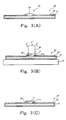
- Figs. 3(A) to 3(C) illustrate a process chart showing an example of a manufacturing method for the metal tag.
- Liquid or sheet-like underfill 24 that is a thermosetting adhesive is supplied to that area 23 of the substrate 20 on which the IC chip 11 will be mounted (Fig. 3 (A)).
- the IC chip 11 is placed on the area 23 and then heated and pressurized together with the substrate 20 by being held between a heating stage 31 and a heating head 32. Consequently, the IC chip 11 and antenna metal pattern 22 are electrically connected via the bumps 11a and the IC chip 11 is fastened to the substrate 20 as the underfill 24 hardens (Fig. 3(B)).
- the RFID tag with the structure shown in Fig. 3(C) is manufactured.
- the IC chip 11 conducts wireless communications with external devices via a loop antenna which makes a round, surrounding the front and back surfaces of the dielectric plate 21.
- the RFID tag of this type is known as a metal tag. For example, even if a metal strip is brought close to the back side of the substrate 20, the front side on which the IC chip 11 is mounted maintains sufficient communications performance.
- the RFID tag produced by the manufacturing method described with reference to Figs. 2(A)-2(B) and 3(A)-3(C) is difficult to make flat and thin because the IC chip 11 mounted on the substrate 20 protrudes from the surface of the substrate 20.
- the present invention has been made in view of the above circumstances and seeks to provide a method for manufacturing a thin and flat RFID tag which advantageously offers the performance of a metal tag as well as the RFID tag produced by the manufacturing method.
- the strap is connected by being mounted on the substrate in the position and orientation in which the IC chip is housed in the recess formed on the substrate. Since the IC chip is housed in the recess, it is possible to make the RFID tag thin and flat.
- the preparation step may have:
- the circuit chip mounting step may apply a thermosetting adhesive to that part of the strap sheet on which the circuit chips are to be mounted, heat and pressurize the part after mounting the circuit chips on the part, and thereby connect the circuit chips to the connector metal patterns on the strap sheet and fasten the circuit chips to the strap sheet.
- the strap parts preparation step, circuit chip mounting step, and strap forming step make it possible to prepare the strap efficiently.
- the preparation step may include:
- the preparation step may include:
- connection step may apply a conductive paste to both ends of the antenna metal pattern on both sides of the recess, heat the strap by mounting the strap on the substrate in the position and orientation in which the circuit chip on the strap is housed in the recess, and thereby connect the connector metal pattern on the strap to both ends of the antenna metal pattern on the substrate.
- the first RFID tag preferably has a structure in which the IC chip is housed in the recess on the substrate, making the RFID tag thin and flat.
- the chip is housed in the recess on the substrate, it is possible to make the RFID tag thin and flat.
- the first manufacturing method since there are two metal patterns, namely, the connector metal pattern and antenna metal pattern, error may occur in antenna length when connecting the two metal patterns with each other as described later with reference to Fig. 11 although on rare occasions.
- the entire part of the metal pattern which acts as an antenna is formed integrally with the tag sheet, preventing introduction of error in the antenna length during manufacture and thereby making it possible to maintain high communications performance.
- the conductive material on the substrate does not cause error in the antenna length.
- a conductive adhesive must be applied in the process of fastening the strap to the substrate and a conductive adhesive in paste form is used after being adjusted to a low level of viscosity for the convenience of application. Consequently, when the strap is pressed against the substrate, the adhesive may form climb-up 134a or squeeze-out 134b as shown in Fig. 12 (Fig. 12 will be described later) although on rare occasions.
- the second manufacturing method advantageously allows the adhesive to be applied to the entire surface of the substrate in advance, making it possible to use an adhesive with high viscosity and low flowability and thereby mitigating the problems described later with reference to Fig. 12.
- the second RFID tag manufacturing method advantageously provides a highly reliable RFID tag manufacturing method which can produce thin and flat RFID tags.
- the pressing step and bending step may be provided either simultaneously or one after the other in any order.
- the bending step bends the tag sheet by fitting the tag sheet in a die.
- the bending step bends the tag sheet and presses the tag sheet against the second surface using a roll.
- preferred embodiments of the present invention provide a thin and flat RFID tag.
- the second RFID tag manufacturing method according to the present invention provides the second RFID tag which is more reliable than the first RFID tag.
- Figs. 4(A) and 4(B) are perspective views showing parts used in a first RFID tag manufacturing method.
- the first manufacturing method prepares a strap 120 shown in Fig. 4(A) and a substrate 130 shown in Fig. 4(B).
- the strap 120 shown in Fig. 4(A) includes a connector metal pattern 122 formed on a base 121 made of a PET film or the like and an IC chip 11 mounted on the base 121 and electrically connected with the connector metal pattern 122.
- the IC chip 11 has gold bumps formed on it and has capability to conduct wireless communications with external devices via an antenna described later (see Fig. 1).
- the substrate 130 in Fig. 4(B) includes a dielectric plate 131 on which a recess 133 is formed to house the IC chip 11 and an antenna metal pattern 132 is formed making a round excluding the recess 133 by going around front and back surfaces.
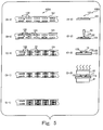
- Fig. 5 is a process chart showing the strap manufacturing method.
- a long strap sheet 120A is prepared.
- the strap sheet 120A includes multiple connector metal patterns 122 formed on a long base 121 made of a PET film or the like.
- Part (A-2) of Fig. 5 is a sectional view of one connector metal pattern on the strap sheet 120A.
- the connector metal pattern 122 consists of two strips, between which an IC chip is mounted.
- liquid or sheet-like underfill 123-- which is a thermosetting adhesive--is supplied to the IC chip mounting positions of the connector metal patterns 122 formed on the strap sheet 120A (see Parts (B-1) and (B-2) of Fig. 5).
- liquid underfill 123 is dripped through a nozzle 33.
- the IC chips 11 are placed on the underfill 123 (see Parts (C-1) and (C-2) of Fig. 5), and heated and pressurized by being held between the heating stage 31 and heating head 32 (see Parts (D-1) and (D-2) of Fig. 5). Consequently, the IC chips 11 are electrically connected with the connector metal patterns 122 via bumps 11a, and then fastened to the strap sheet 120A as the underfill 123 hardens.
- the strap sheet 120A is diced by blanking or cutting into individual straps 120 containing an IC chip 11 and a connector metal pattern 122 (see Fig. 4(A)).
- the manufacturing method of the substrate 130 is a method of efficiently manufacturing multiple substrates 130 and composed of two or more processes. There will be described below an example that three substrates 130 are manufactured.
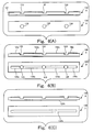
- Figs. 6(A) through 6(C) are diagrams showing a first process in the manufacturing method of the substrate 130.
- the front and back surfaces of the dielectric plate 131 are covered with metal foil for forming a metal pattern.
- a plate member 130A having three recesses 133 formed on one surface thereof is thus prepared.
- the surface where the three recesses 133 are formed will be referred to as “top surface,” while the other surface opposite the top surface will be referred to as “bottom surface.”
- That part of the antenna metal pattern 132 shown in Fig. 4(B) which serves as pattern portions 132b for three substrates 130 is formed on the bottom surface of the plate member 130A, opposite the top surface where the recesses 133 are formed.
- the pattern portions 132b are integrally formed as a continuous line covering the three substrates 130.
- the pattern portions 132b are also formed by etching.
- This first process is efficient because the pattern portions 132a for three substrates 130 are formed on the top surface at a time by the first etching, and the pattern portions 132b for three substrates 130 are formed on the bottom surface at a time by the second etching.
- the manufacturing method of the substrate 130 proceeds to the next process.
- Figs. 7(A) and 7(B) are diagrams showing a second process and a third process in the manufacturing method of the substrate 130, respectively.
- a through hole 130A_1 piercing through the plate member 130A is formed at a position that corresponds to each of both edges of the dielectric plate 131 along which the antenna metal pattern 132 is to run in the substrate 130 shown in Fig. 4 (B).
- the hole 130A_1 is formed for each of the three substrates 130.
- each through hole 130A_1 is plated with metal of the same kind as the metal forming each pattern portion.
- plating an inner wall of one through hole 130A_1 forms two pattern portions 132c of the respective adjacent antenna metal patterns 132 at the same time, which is efficient.
- each substrate 130 as shown in Fig. 4(B) is completed in the next process.
- Fig. 8 is a diagram showing a fourth process in the manufacturing method of the substrate 130.
- the plate member 130A where the three antenna metal patterns 132 are formed is cut into three pieces along cutting-plane lines passing through the plated through holes 130A_1 and then trimmed.
- three substrates 130 as shown in Fig. 4(B) are completed.
- the manufacturing method of the substrate may be such a method that the through hole 130A_1 is formed and plated first and then, the pattern portion 132a on the top surface and the pattern portion 132b on the bottom surface are formed.
- Figs. 9(A) to 9(C) illustrate a process chart showing the RFID tag manufacturing method which uses the strap 120 and substrate 130 shown in Figs. 4(A) and 4(B).
- thermosetting conductive adhesive 134 is supplied to both ends of the antenna metal pattern 132 on both sides of the recess 133 on the substrate 130 through a dispenser nozzle 34 (Fig. 9(A)).
- a conductive paste for connection may be printed instead of the supply through the nozzle 34.
- the strap 120 is turned upside down and mounted on the substrate 130 with the antenna metal pattern 132 on the substrate 130 aligned with the IC chip 11 on the strap 120 (Fig. 6(B)).
- the conductive adhesive is hardened by heating, the connector metal pattern 122 on the strap 120 and the antenna metal pattern 132 on the substrate 130 are electrically connected with each other with the IC chip 11 housed in the recess 133 on the substrate 130 and the strap 120 is fastened to the substrate 130 (Fig. 9(C)).
- the substrate 130 and strap 120 maybe pressurized by being pinched.
- the connector metal pattern 122 on the strap 120 and the antenna metal pattern 132 on the substrate 130 form a loop antenna which makes a round, surrounding the front and back surfaces of the dielectric plate 131 and via which the IC chip 11 conducts wireless communications with external devices.
- Fig. 10 is a sectional view of a RFID tag produced by the RFID tag manufacturing method.
- the IC chip 11 is housed in the recess 133 on the substrate 130, making the RFID tag thinner and flatter than the conventional example described with reference to Figs. 2 (A) -2 (B) and 3(A)-3(C).
- Fig. 11 is a diagram showing one of the problems encountered on rare occasions with RFID tags produced by the RFID tag manufacturing method shown in Figs. 4(A) to 9(C).
- the strap 120 may tilt on the substrate 130 as shown in Fig. 11. If the strap 120 is mounted in a tilted condition, the loop antenna formed by the connector metal pattern 122 on the strap 120 and the antenna metal pattern 132 on the substrate 130 will deviate from its normal length, which may affect communications functions.
- Fig. 12 is a diagram showing another problem encountered on rare occasions with RFID tags produced by the RFID tag manufacturing method shown in Figs. 4(A) to 9(C).
- Fig. 12 is an enlarged view of a bonded portion between the substrate 130 and strap 120.
- the conductive adhesive 134 in paste form (see Fig. 9(A)) is used when mounting and fastening the strap 120 onto the substrate 130, but it is difficult to accurately control application quantity of the conductive adhesive 134, which is in paste form, in the process shown in Fig. 9(A). A little excess application may cause the conductive adhesive to form climb-up 134a above the strap 120 or squeeze-out 134b inside the recess 133 as shown in Fig. 12.
- climb-up 134a may cause print defects.
- squeeze-out 134b inside the recess 133 may cause a short circuit with the IC chip 11, resulting in a malfunction.
- RFID tags which encounter any of the problems described with reference to Figs. 11 and 12 may be removed in the process of inspection, but it is preferable to increase manufacturing reliability.
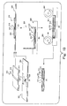
- Fig. 13 is a diagram showing an embodiment of a second RFID tag manufacturing method according to the present invention and a RFID tag produced by this manufacturing method.
- a substrate 310 and a tag sheet 320 are prepared (Parts (A) and (B) of Fig. 13).
- the substrate 310 consists of a plastic plate 311 with a hole 314 (see Part (C) of Fig. 13) formed to house an IC chip 11. Furthermore, an adhesive 312 is applied to around the substrate 310, and a conductive material 313 such as a conductive sheet or conductive adhesive is applied to a seam of an antenna.
- the tag sheet 320 consists of a metal pattern 322 which, being formed on a base 321 made of a PET film or the like, acts as an antenna after manufacture and an IC chip 11 mounted on the base 321 by thermocompression bonding or by solder reflow.
- the metal pattern 322 has a design different from that of the metal pattern 132 (see Fig. 4(B)) according to the above embodiment. This is because an optimal pattern is selected according to combination with the IC chip 11, uses, and the like.
- a first surface of the substrate 310 on which the recess 314 is formed is pressed against that position on the tag sheet 320 where the IC chip 11 is housed in the recess 314 on the substrate 310, and consequently the tag sheet 320 is affixed to the first surface with the adhesive 312 applied to the substrate 310 (Part (C) of Fig. 13).
- the tag sheet 320 with which the first surface of the substrate 310 connected is fitted in a die 350 in which a recess 351 of an appropriate size is formed, and consequently, that part of the tag sheet 320 which sticks out of the substrate 310 is bent along edges of the substrate 310 (Part (D) of Fig. 13).
- the tag sheet 320 may be fitted alone in the die 350 and bent as shown in Part (D) of Fig. 13, before mounting and bonding the substrate 310 onto it.
- the tag sheet 320 positioned on the die 350 may be pushed into the recess 351 of the die 350 by the substrate 310 to mount the substrate 310 on the tag sheet 320 and bend the tag sheet 320 simultaneously.
- the tag sheet 320 After being processed to the condition shown in Part (D) of Fig. 13, the tag sheet 320 is bent along the edges of the substrate 310 by a roller 360 so as to fold down onto the second surface which is opposite the first surface of the substrate 310 on which the recess 314 is formed, the tag sheet 320 is bonded to the second surface, and both ends of the metal pattern 322 on the tag sheet 320 are connected by the conductive material 313 (Part (E) of Fig. 13).
- the manufacturing method shown in Fig. 13 not only produces thin and flat RFID tags as with the embodiment described earlier, but also eliminates the problem of increased antenna length described with reference to Figs. 11 and 12 as well as further improves reliability.
- the manufacturing method shown in Fig. 13 eliminates the need for such a process. Also, the manufacturing method shown in Fig. 13 does not need the process of forming a metal pattern on a substrate, which is more complex and costly than the process of applying an adhesive or conductive material on the substrate. In this way, the manufacturing method shown in Fig. 13 requires a smaller number of processes and costs less than the manufacturing method described earlier.
Landscapes
- Engineering & Computer Science (AREA)
- Microelectronics & Electronic Packaging (AREA)
- Physics & Mathematics (AREA)
- Computer Hardware Design (AREA)
- General Physics & Mathematics (AREA)
- Theoretical Computer Science (AREA)
- Electromagnetism (AREA)
- Details Of Aerials (AREA)
Applications Claiming Priority (3)
| Application Number | Priority Date | Filing Date | Title |
|---|---|---|---|
| JP2006034026 | 2006-02-10 | ||
| JP2006074260 | 2006-03-17 | ||
| JP2006227359A JP5034371B2 (ja) | 2006-02-10 | 2006-08-24 | Rfidタグの製造方法およびrfidタグ |
Publications (3)
| Publication Number | Publication Date |
|---|---|
| EP1818861A2 true EP1818861A2 (de) | 2007-08-15 |
| EP1818861A3 EP1818861A3 (de) | 2007-09-05 |
| EP1818861B1 EP1818861B1 (de) | 2009-12-23 |
Family
ID=37946680
Family Applications (1)
| Application Number | Title | Priority Date | Filing Date |
|---|---|---|---|
| EP07250266A Not-in-force EP1818861B1 (de) | 2006-02-10 | 2007-01-23 | Verfahren zur Herstellung von einem RFID-Etikett und RFID-Etikett |
Country Status (6)
| Country | Link |
|---|---|
| US (2) | US7954228B2 (de) |
| EP (1) | EP1818861B1 (de) |
| JP (1) | JP5034371B2 (de) |
| KR (1) | KR100825524B1 (de) |
| DE (1) | DE602007003867D1 (de) |
| TW (1) | TWI330814B (de) |
Cited By (4)
| Publication number | Priority date | Publication date | Assignee | Title |
|---|---|---|---|---|
| EP2056239A1 (de) * | 2007-10-29 | 2009-05-06 | China Steel Corporation | Radiofrequenzidentifikationsetikettvorrichtung für metallische Produkte |
| WO2009102708A1 (en) * | 2008-02-14 | 2009-08-20 | 3M Innovative Properties Company | Radio frequency identification (rfid) tag including a three-dimensional loop antenna |
| WO2011033172A1 (en) | 2009-09-18 | 2011-03-24 | Valtion Teknillinen Tutkimuskeskus | Antenna construction, for example for an rfid transponder system |
| EP3490067A4 (de) * | 2016-07-22 | 2020-02-19 | KYOCERA Corporation | Substrat für rfid-etiketten, rfid-etikett und rfid-system |
Families Citing this family (38)
| Publication number | Priority date | Publication date | Assignee | Title |
|---|---|---|---|---|
| US9117128B2 (en) | 2005-12-09 | 2015-08-25 | Tego, Inc. | External access to memory on an RFID tag |
| US9361568B2 (en) | 2005-12-09 | 2016-06-07 | Tego, Inc. | Radio frequency identification tag with hardened memory system |
| US9418263B2 (en) | 2005-12-09 | 2016-08-16 | Tego, Inc. | Operating systems for an RFID tag |
| US9542577B2 (en) | 2005-12-09 | 2017-01-10 | Tego, Inc. | Information RFID tagging facilities |
| US9430732B2 (en) * | 2014-05-08 | 2016-08-30 | Tego, Inc. | Three-dimension RFID tag with opening through structure |
| US8947233B2 (en) | 2005-12-09 | 2015-02-03 | Tego Inc. | Methods and systems of a multiple radio frequency network node RFID tag |
| US8988223B2 (en) | 2005-12-09 | 2015-03-24 | Tego Inc. | RFID drive management facility |
| JP5034371B2 (ja) * | 2006-02-10 | 2012-09-26 | 富士通株式会社 | Rfidタグの製造方法およびrfidタグ |
| GB2446604A (en) * | 2007-02-14 | 2008-08-20 | Thomas Fergus Hughes | A tag for laboratory sample cassette |
| US7949310B2 (en) * | 2007-03-26 | 2011-05-24 | Broadcom Corporation | RF filtering at very high frequencies for substrate communications |
| FR2918485B1 (fr) * | 2007-07-04 | 2010-09-10 | Arjowiggins Licensing Sas | Support fibreux pour insert comportant une antenne |
| EP2071906A1 (de) * | 2007-12-13 | 2009-06-17 | Gemplus | Verfahren zur Herstellung einer Vorrichtung, die mindestens zwei verschiedene Komponenten umfasst, die durch Verbindungsdrähte miteinander verbunden sind, und so erhaltene Vorrichtung |
| EP2248074B1 (de) * | 2008-02-26 | 2016-05-25 | Avery Dennison Corporation | Rfid-etikett für direkten und indirekten lebensmittelkontakt |
| KR101006870B1 (ko) * | 2008-05-02 | 2011-01-12 | 유인종 | 안테나 코일과 집적회로 칩을 구비한 카드에 칩을인레이하는 방법 |
| CZ303919B6 (cs) * | 2009-04-22 | 2013-06-26 | Ceské vysoké ucení technické v Praze, Fakulta elektrotechnická | Nízkoprofilová sterbinová anténa |
| JP5896594B2 (ja) * | 2010-05-14 | 2016-03-30 | 株式会社村田製作所 | 無線icデバイス |
| US8584955B2 (en) * | 2010-09-17 | 2013-11-19 | Apple Inc. | Systems and methods for integrating radio-frequency identification circuitry into flexible circuits |
| US9325053B2 (en) * | 2010-11-08 | 2016-04-26 | Smartrac Ip B.V. | Method for producing a radio frequency identification (RFID) transponder |
| CN103548038B (zh) | 2011-04-07 | 2017-02-15 | 能通 | 无线识别标签、具有该标签的电子产品pcb、以及电子产品管理系统 |
| WO2012157596A1 (ja) * | 2011-05-16 | 2012-11-22 | 株式会社村田製作所 | 無線icデバイス |
| US8671772B2 (en) * | 2011-09-22 | 2014-03-18 | Hana Micron America, Inc. | Quality assurance and reliability testing apparatus for RFID tags |
| US9224695B2 (en) | 2013-02-28 | 2015-12-29 | Infineon Technologies Ag | Chip arrangement and a method for manufacturing a chip arrangement |
| US9953193B2 (en) | 2014-09-30 | 2018-04-24 | Tego, Inc. | Operating systems for an RFID tag |
| WO2017141663A1 (ja) * | 2016-02-17 | 2017-08-24 | 株式会社村田製作所 | 無線通信デバイス、及びその製造方法 |
| US11618191B2 (en) | 2016-07-27 | 2023-04-04 | Composecure, Llc | DI metal transaction devices and processes for the manufacture thereof |
| US10977540B2 (en) | 2016-07-27 | 2021-04-13 | Composecure, Llc | RFID device |
| CN109564634B (zh) | 2016-07-27 | 2026-04-14 | 安全创造有限责任公司 | 用于交易卡的经包覆模制的电子部件及其制造方法 |
| US10762412B2 (en) | 2018-01-30 | 2020-09-01 | Composecure, Llc | DI capacitive embedded metal card |
| JP6776847B2 (ja) * | 2016-11-24 | 2020-10-28 | 富士通株式会社 | ループアンテナ及び電子機器 |
| NZ762589A (en) | 2017-09-07 | 2022-05-27 | Composecure Llc | Transaction card with embedded electronic components and process for manufacture |
| US11151437B2 (en) | 2017-09-07 | 2021-10-19 | Composecure, Llc | Metal, ceramic, or ceramic-coated transaction card with window or window pattern and optional backlighting |
| KR102931665B1 (ko) | 2017-10-18 | 2026-02-26 | 컴포시큐어 엘.엘.씨. | 윈도우 또는 윈도우 패턴 및 선택적인 백라이팅을 갖는 금속, 세라믹, 또는 세라믹 코팅된 트랜잭션 카드 |
| DE102018117364A1 (de) * | 2018-07-18 | 2020-01-23 | Infineon Technologies Ag | Verfahren und Vorrichtung zum Trimmen einer auf einem Träger aufgebrachten Antenne, Verfahren zum Herstellen einer Trägerstruktur, Trägerstruktur und Chipkarte |
| DE102019128779B4 (de) * | 2019-10-24 | 2021-05-12 | Infineon Technologies Ag | Hochfrequenz-Vorrichtung mit Hochfrequenz-Signalführungselement und zugehöriges Herstellungsverfahren |
| CN115087985B (zh) | 2019-12-28 | 2025-07-18 | 艾利丹尼森零售信息服务有限公司 | 与电抗型连接带联用的调谐组件方法和系统 |
| EP4081944B1 (de) | 2019-12-28 | 2024-07-10 | Avery Dennison Retail Information Services LLC | Verfahren zur herstellung eines radiofrequenz-identifikationsetiketts |
| USD1032613S1 (en) * | 2020-02-02 | 2024-06-25 | Federal Card Services, LLC | Smart card |
| USD948613S1 (en) | 2020-04-27 | 2022-04-12 | Composecure, Llc | Layer of a transaction card |
Citations (3)
| Publication number | Priority date | Publication date | Assignee | Title |
|---|---|---|---|---|
| US20040125040A1 (en) | 2002-12-31 | 2004-07-01 | Ferguson Scott Wayne | RFID device and method of forming |
| EP1498842A1 (de) | 2002-04-01 | 2005-01-19 | K-Ubique ID Corporation | Kommunikationsgerät und gehäuse dafür |
| US20050179552A1 (en) | 2002-09-30 | 2005-08-18 | The Furukawa Electric Co., Ltd. | RFID tag and its manufacturing method |
Family Cites Families (28)
| Publication number | Priority date | Publication date | Assignee | Title |
|---|---|---|---|---|
| US4783646A (en) * | 1986-03-07 | 1988-11-08 | Kabushiki Kaisha Toshiba | Stolen article detection tag sheet, and method for manufacturing the same |
| ZA941671B (en) * | 1993-03-11 | 1994-10-12 | Csir | Attaching an electronic circuit to a substrate. |
| EP0824112B1 (de) * | 1996-08-13 | 2006-05-10 | Basell Polyolefine GmbH | Geträgerte chemische Verbindung |
| DE69838473T2 (de) | 1997-12-25 | 2008-01-17 | Nihon Kohden Corp. | Gerät zur Übertragung von biologischen Signalen |
| JP3656184B2 (ja) * | 1997-12-25 | 2005-06-08 | 日本光電工業株式会社 | 生体信号送信装置 |
| US6856832B1 (en) | 1997-12-25 | 2005-02-15 | Nihon Kohden Corporation | Biological signal detection apparatus Holter electrocardiograph and communication system of biological signals |
| JP3951409B2 (ja) * | 1998-02-12 | 2007-08-01 | 日立化成工業株式会社 | Icカードとその製造法 |
| US6107920A (en) * | 1998-06-09 | 2000-08-22 | Motorola, Inc. | Radio frequency identification tag having an article integrated antenna |
| JP2000311226A (ja) | 1998-07-28 | 2000-11-07 | Toshiba Corp | 無線icカード及びその製造方法並びに無線icカード読取り書込みシステム |
| JP2000165127A (ja) * | 1998-11-27 | 2000-06-16 | Furukawa Electric Co Ltd:The | 薄型平面アンテナ |
| JP3502557B2 (ja) | 1999-01-07 | 2004-03-02 | 松下電器産業株式会社 | 非接触icカードの製造方法 |
| US6891110B1 (en) | 1999-03-24 | 2005-05-10 | Motorola, Inc. | Circuit chip connector and method of connecting a circuit chip |
| CA2302957C (en) * | 1999-03-24 | 2009-06-30 | Morgan Adhesives Company | Circuit chip connector and method of connecting a circuit chip |
| JP2001202488A (ja) * | 2000-01-20 | 2001-07-27 | Matsushita Electric Ind Co Ltd | 非接触icタグ |
| JP4620836B2 (ja) | 2000-06-08 | 2011-01-26 | 大日本印刷株式会社 | ウエハーの製造方法 |
| JP2002083832A (ja) * | 2000-09-08 | 2002-03-22 | Toppan Forms Co Ltd | Icチップの固定方法 |
| JP4028224B2 (ja) * | 2001-12-20 | 2007-12-26 | 大日本印刷株式会社 | 非接触通信機能を有する紙製icカード用基材 |
| DE102004004469A1 (de) * | 2003-12-22 | 2005-08-18 | Smartrac Technology Ltd. | Verfahren zur Herstellung eines Sicherheitslagenaufbaus sowie Sicherheitslagenaufbau und einen solchen enthaltende Identifikationsdokumente |
| JP4567988B2 (ja) * | 2004-02-05 | 2010-10-27 | 株式会社日立製作所 | 紙状rfidタグおよびその製造方法 |
| JP2005309520A (ja) * | 2004-04-16 | 2005-11-04 | Dainippon Printing Co Ltd | インターポーザー付シート、その巻体およびその検査方法 |
| US7292148B2 (en) * | 2004-06-18 | 2007-11-06 | Avery Dennison Corporation | Method of variable position strap mounting for RFID transponder |
| JP2006031336A (ja) * | 2004-07-15 | 2006-02-02 | Fujitsu Ltd | Rfidタグの製造方法 |
| JP4653440B2 (ja) * | 2004-08-13 | 2011-03-16 | 富士通株式会社 | Rfidタグおよびその製造方法 |
| US20070040686A1 (en) * | 2005-08-16 | 2007-02-22 | X-Cyte, Inc., A California Corporation | RFID inlays and methods of their manufacture |
| US20070040688A1 (en) * | 2005-08-16 | 2007-02-22 | X-Cyte, Inc., A California Corporation | RFID inlays and methods of their manufacture |
| JP5034371B2 (ja) * | 2006-02-10 | 2012-09-26 | 富士通株式会社 | Rfidタグの製造方法およびrfidタグ |
| US7546671B2 (en) * | 2006-09-26 | 2009-06-16 | Micromechanic And Automation Technology Ltd. | Method of forming an inlay substrate having an antenna wire |
| US7701352B2 (en) * | 2006-11-22 | 2010-04-20 | Avery Dennison Corporation | RFID label with release liner window, and method of making |
-
2006
- 2006-08-24 JP JP2006227359A patent/JP5034371B2/ja not_active Expired - Fee Related
-
2007
- 2007-01-19 TW TW096102071A patent/TWI330814B/zh not_active IP Right Cessation
- 2007-01-23 EP EP07250266A patent/EP1818861B1/de not_active Not-in-force
- 2007-01-23 DE DE602007003867T patent/DE602007003867D1/de active Active
- 2007-02-05 US US11/702,168 patent/US7954228B2/en not_active Expired - Fee Related
- 2007-02-09 KR KR1020070013848A patent/KR100825524B1/ko not_active Expired - Fee Related
-
2011
- 2011-03-21 US US13/064,346 patent/US8698633B2/en not_active Expired - Fee Related
Patent Citations (3)
| Publication number | Priority date | Publication date | Assignee | Title |
|---|---|---|---|---|
| EP1498842A1 (de) | 2002-04-01 | 2005-01-19 | K-Ubique ID Corporation | Kommunikationsgerät und gehäuse dafür |
| US20050179552A1 (en) | 2002-09-30 | 2005-08-18 | The Furukawa Electric Co., Ltd. | RFID tag and its manufacturing method |
| US20040125040A1 (en) | 2002-12-31 | 2004-07-01 | Ferguson Scott Wayne | RFID device and method of forming |
Cited By (11)
| Publication number | Priority date | Publication date | Assignee | Title |
|---|---|---|---|---|
| EP2056239A1 (de) * | 2007-10-29 | 2009-05-06 | China Steel Corporation | Radiofrequenzidentifikationsetikettvorrichtung für metallische Produkte |
| US8179264B2 (en) | 2007-10-29 | 2012-05-15 | China Steel Corporation | Radio frequency identification tag device for metallic products |
| WO2009102708A1 (en) * | 2008-02-14 | 2009-08-20 | 3M Innovative Properties Company | Radio frequency identification (rfid) tag including a three-dimensional loop antenna |
| WO2009102714A3 (en) * | 2008-02-14 | 2010-05-27 | 3M Innovative Properties Company | Radio frequency identification (rfid) tag including a three-dimensional loop antenna |
| US7847697B2 (en) | 2008-02-14 | 2010-12-07 | 3M Innovative Properties Company | Radio frequency identification (RFID) tag including a three-dimensional loop antenna |
| US7982616B2 (en) | 2008-02-14 | 2011-07-19 | 3M Innovative Properties Company | Radio frequency identification (RFID) tag including a three-dimensional loop antenna |
| TWI553964B (zh) * | 2008-02-14 | 2016-10-11 | 3M新設資產公司 | 具有三維迴路天線之射頻辨識標籤 |
| WO2011033172A1 (en) | 2009-09-18 | 2011-03-24 | Valtion Teknillinen Tutkimuskeskus | Antenna construction, for example for an rfid transponder system |
| US9082058B2 (en) | 2009-09-18 | 2015-07-14 | Teknologian Tutkimuskeskus Vtt | Antenna construction, for example for an RFID transponder system |
| US9502749B2 (en) | 2009-09-18 | 2016-11-22 | Teknologian Tutkimuskeskus Vtt Oy | Antenna construction, for example for an RFID transponder system |
| EP3490067A4 (de) * | 2016-07-22 | 2020-02-19 | KYOCERA Corporation | Substrat für rfid-etiketten, rfid-etikett und rfid-system |
Also Published As
| Publication number | Publication date |
|---|---|
| DE602007003867D1 (de) | 2010-02-04 |
| US20070193021A1 (en) | 2007-08-23 |
| TWI330814B (en) | 2010-09-21 |
| US8698633B2 (en) | 2014-04-15 |
| TW200805171A (en) | 2008-01-16 |
| KR20070081447A (ko) | 2007-08-16 |
| US20110168789A1 (en) | 2011-07-14 |
| EP1818861A3 (de) | 2007-09-05 |
| JP5034371B2 (ja) | 2012-09-26 |
| KR100825524B1 (ko) | 2008-04-25 |
| JP2007280343A (ja) | 2007-10-25 |
| US7954228B2 (en) | 2011-06-07 |
| EP1818861B1 (de) | 2009-12-23 |
Similar Documents
| Publication | Publication Date | Title |
|---|---|---|
| EP1818861B1 (de) | Verfahren zur Herstellung von einem RFID-Etikett und RFID-Etikett | |
| CN100538731C (zh) | Rfid标签制造方法和rfid标签 | |
| JP4855849B2 (ja) | Rfidタグの製造方法、およびrfidタグ | |
| US20080001759A1 (en) | RFID tag manufacturing method and RFID tag | |
| EP1956873B1 (de) | RFID-Etikett und Herstellungsverfahren dafür | |
| US6552694B1 (en) | Semiconductor device and fabrication method thereof | |
| KR20060015233A (ko) | Rfid 태그 및 그 제조 방법 | |
| CN104978595A (zh) | 双接口ic卡组件及用于制造双接口ic卡组件的方法 | |
| US8127997B2 (en) | Method for mounting an electronic component on a substrate | |
| CN100481122C (zh) | Rfid标签及其制造方法 | |
| US7431218B2 (en) | RFID tag, module component, and RFID tag fabrication method | |
| US7317395B2 (en) | RFID tag and method of manufacturing the same | |
| JP5344267B2 (ja) | Rfidタグの製造方法およびrfidタグ | |
| EP1804203A2 (de) | RFID-Etikett | |
| KR101098289B1 (ko) | Rfid 태그, 이의 제작방법, 이를 이용한 패키징 구조체 및 제작방법 | |
| EP3079105B1 (de) | Chipkarte mit doppelschnittstellenkomponenten und verfahren zur herstellung der chipkarte mit doppelschnittstellenkomponenten | |
| EP2053548A1 (de) | RFID-Etikett und Herstellungsverfahren dafür | |
| EP1947918A2 (de) | Elektronische Vorrichtung und Herstellungsverfahren dafür | |
| JP2003091709A (ja) | Icカード及びその製造方法 | |
| HK1234185B (en) | Method for producing a circuit for a chip card module and circuit for a chip card module |
Legal Events
| Date | Code | Title | Description |
|---|---|---|---|
| PUAI | Public reference made under article 153(3) epc to a published international application that has entered the european phase |
Free format text: ORIGINAL CODE: 0009012 |
|
| PUAL | Search report despatched |
Free format text: ORIGINAL CODE: 0009013 |
|
| AK | Designated contracting states |
Kind code of ref document: A2 Designated state(s): AT BE BG CH CY CZ DE DK EE ES FI FR GB GR HU IE IS IT LI LT LU LV MC NL PL PT RO SE SI SK TR |
|
| AX | Request for extension of the european patent |
Extension state: AL BA HR MK YU |
|
| AK | Designated contracting states |
Kind code of ref document: A3 Designated state(s): AT BE BG CH CY CZ DE DK EE ES FI FR GB GR HU IE IS IT LI LT LU LV MC NL PL PT RO SE SI SK TR |
|
| AX | Request for extension of the european patent |
Extension state: AL BA HR MK YU |
|
| RIC1 | Information provided on ipc code assigned before grant |
Ipc: H01Q 7/00 20060101ALI20070730BHEP Ipc: G06K 19/077 20060101AFI20070427BHEP Ipc: H01Q 1/38 20060101ALI20070730BHEP |
|
| 17P | Request for examination filed |
Effective date: 20080227 |
|
| AKX | Designation fees paid |
Designated state(s): DE FR GB |
|
| GRAP | Despatch of communication of intention to grant a patent |
Free format text: ORIGINAL CODE: EPIDOSNIGR1 |
|
| GRAS | Grant fee paid |
Free format text: ORIGINAL CODE: EPIDOSNIGR3 |
|
| GRAA | (expected) grant |
Free format text: ORIGINAL CODE: 0009210 |
|
| AK | Designated contracting states |
Kind code of ref document: B1 Designated state(s): DE FR GB |
|
| REG | Reference to a national code |
Ref country code: GB Ref legal event code: FG4D |
|
| REF | Corresponds to: |
Ref document number: 602007003867 Country of ref document: DE Date of ref document: 20100204 Kind code of ref document: P |
|
| PLBE | No opposition filed within time limit |
Free format text: ORIGINAL CODE: 0009261 |
|
| STAA | Information on the status of an ep patent application or granted ep patent |
Free format text: STATUS: NO OPPOSITION FILED WITHIN TIME LIMIT |
|
| 26N | No opposition filed |
Effective date: 20100924 |
|
| REG | Reference to a national code |
Ref country code: FR Ref legal event code: PLFP Year of fee payment: 10 |
|
| REG | Reference to a national code |
Ref country code: FR Ref legal event code: PLFP Year of fee payment: 11 |
|
| PGFP | Annual fee paid to national office [announced via postgrant information from national office to epo] |
Ref country code: FR Payment date: 20161215 Year of fee payment: 11 |
|
| PGFP | Annual fee paid to national office [announced via postgrant information from national office to epo] |
Ref country code: DE Payment date: 20170117 Year of fee payment: 11 |
|
| PGFP | Annual fee paid to national office [announced via postgrant information from national office to epo] |
Ref country code: GB Payment date: 20170118 Year of fee payment: 11 |
|
| REG | Reference to a national code |
Ref country code: DE Ref legal event code: R119 Ref document number: 602007003867 Country of ref document: DE |
|
| GBPC | Gb: european patent ceased through non-payment of renewal fee |
Effective date: 20180123 |
|
| PG25 | Lapsed in a contracting state [announced via postgrant information from national office to epo] |
Ref country code: FR Free format text: LAPSE BECAUSE OF NON-PAYMENT OF DUE FEES Effective date: 20180131 Ref country code: DE Free format text: LAPSE BECAUSE OF NON-PAYMENT OF DUE FEES Effective date: 20180801 |
|
| REG | Reference to a national code |
Ref country code: FR Ref legal event code: ST Effective date: 20180928 |
|
| PG25 | Lapsed in a contracting state [announced via postgrant information from national office to epo] |
Ref country code: GB Free format text: LAPSE BECAUSE OF NON-PAYMENT OF DUE FEES Effective date: 20180123 |