EP1818982A2 - Anordnung mit mindestens einem Leistungshalbleitermodul und einem Kühlbauteil und zugehöriges Herstellungsverfahren - Google Patents
Anordnung mit mindestens einem Leistungshalbleitermodul und einem Kühlbauteil und zugehöriges Herstellungsverfahren Download PDFInfo
- Publication number
- EP1818982A2 EP1818982A2 EP07002032A EP07002032A EP1818982A2 EP 1818982 A2 EP1818982 A2 EP 1818982A2 EP 07002032 A EP07002032 A EP 07002032A EP 07002032 A EP07002032 A EP 07002032A EP 1818982 A2 EP1818982 A2 EP 1818982A2
- Authority
- EP
- European Patent Office
- Prior art keywords
- power semiconductor
- substrate
- semiconductor module
- housing
- connection elements
- Prior art date
- Legal status (The legal status is an assumption and is not a legal conclusion. Google has not performed a legal analysis and makes no representation as to the accuracy of the status listed.)
- Granted
Links
Images
Classifications
-
- H—ELECTRICITY
- H05—ELECTRIC TECHNIQUES NOT OTHERWISE PROVIDED FOR
- H05K—PRINTED CIRCUITS; CASINGS OR CONSTRUCTIONAL DETAILS OF ELECTRIC APPARATUS; MANUFACTURE OF ASSEMBLAGES OF ELECTRICAL COMPONENTS
- H05K7/00—Constructional details common to different types of electric apparatus
- H05K7/20—Modifications to facilitate cooling, ventilating, or heating
- H05K7/2039—Modifications to facilitate cooling, ventilating, or heating characterised by the heat transfer by conduction from the heat generating element to a dissipating body
- H05K7/20436—Inner thermal coupling elements in heat dissipating housings, e.g. protrusions or depressions integrally formed in the housing
- H05K7/2049—Pressing means used to urge contact, e.g. springs
-
- H—ELECTRICITY
- H05—ELECTRIC TECHNIQUES NOT OTHERWISE PROVIDED FOR
- H05K—PRINTED CIRCUITS; CASINGS OR CONSTRUCTIONAL DETAILS OF ELECTRIC APPARATUS; MANUFACTURE OF ASSEMBLAGES OF ELECTRICAL COMPONENTS
- H05K7/00—Constructional details common to different types of electric apparatus
- H05K7/20—Modifications to facilitate cooling, ventilating, or heating
- H05K7/2089—Modifications to facilitate cooling, ventilating, or heating for power electronics, e.g. for inverters for controlling motor
- H05K7/209—Heat transfer by conduction from internal heat source to heat radiating structure
-
- H—ELECTRICITY
- H10—SEMICONDUCTOR DEVICES; ELECTRIC SOLID-STATE DEVICES NOT OTHERWISE PROVIDED FOR
- H10W—GENERIC PACKAGES, INTERCONNECTIONS, CONNECTORS OR OTHER CONSTRUCTIONAL DETAILS OF DEVICES COVERED BY CLASS H10
- H10W72/00—Interconnections or connectors in packages
-
- H—ELECTRICITY
- H10—SEMICONDUCTOR DEVICES; ELECTRIC SOLID-STATE DEVICES NOT OTHERWISE PROVIDED FOR
- H10W—GENERIC PACKAGES, INTERCONNECTIONS, CONNECTORS OR OTHER CONSTRUCTIONAL DETAILS OF DEVICES COVERED BY CLASS H10
- H10W90/00—Package configurations
-
- H—ELECTRICITY
- H05—ELECTRIC TECHNIQUES NOT OTHERWISE PROVIDED FOR
- H05K—PRINTED CIRCUITS; CASINGS OR CONSTRUCTIONAL DETAILS OF ELECTRIC APPARATUS; MANUFACTURE OF ASSEMBLAGES OF ELECTRICAL COMPONENTS
- H05K1/00—Printed circuits
- H05K1/02—Details
- H05K1/0213—Electrical arrangements not otherwise provided for
- H05K1/0263—High current adaptations, e.g. printed high current conductors or using auxiliary non-printed means; Fine and coarse circuit patterns on one circuit board
-
- H—ELECTRICITY
- H10—SEMICONDUCTOR DEVICES; ELECTRIC SOLID-STATE DEVICES NOT OTHERWISE PROVIDED FOR
- H10W—GENERIC PACKAGES, INTERCONNECTIONS, CONNECTORS OR OTHER CONSTRUCTIONAL DETAILS OF DEVICES COVERED BY CLASS H10
- H10W72/00—Interconnections or connectors in packages
- H10W72/50—Bond wires
- H10W72/531—Shapes of wire connectors
- H10W72/5363—Shapes of wire connectors the connected ends being wedge-shaped
-
- H—ELECTRICITY
- H10—SEMICONDUCTOR DEVICES; ELECTRIC SOLID-STATE DEVICES NOT OTHERWISE PROVIDED FOR
- H10W—GENERIC PACKAGES, INTERCONNECTIONS, CONNECTORS OR OTHER CONSTRUCTIONAL DETAILS OF DEVICES COVERED BY CLASS H10
- H10W90/00—Package configurations
- H10W90/701—Package configurations characterised by the relative positions of pads or connectors relative to package parts
- H10W90/751—Package configurations characterised by the relative positions of pads or connectors relative to package parts of bond wires
- H10W90/754—Package configurations characterised by the relative positions of pads or connectors relative to package parts of bond wires between a chip and a stacked insulating package substrate, interposer or RDL
Definitions
- the invention describes an arrangement with at least one power semiconductor module in pressure contact design and with a cooling component and an associated manufacturing method.
- a starting point of the invention form power semiconductor modules as exemplified by DE 197 19 703 A1 are known.
- Such power semiconductor modules consist of a housing with at least one electrically insulating substrate arranged therein, preferably for direct mounting on a cooling component.
- the substrate in turn consists of an insulating body with a plurality of mutually insulated metallic interconnect tracks located thereon and power semiconductor components located thereon and connected in a circuitally correct manner to these interconnect tracks.
- the known power semiconductor modules have connection elements for external load and auxiliary connections as well as connecting elements arranged in the interior. These connecting elements for circuit-compatible connections in the interior of the power semiconductor module are usually designed as Drahtbonditatien.
- the pressure device has a stable, preferably metallic, pressure element for pressure build-up, an elastic cushion element for pressure storage and a bridge element for pressure introduction onto separate regions of the substrate surface.
- the bridge element is preferably configured as a plastic molded body with a surface facing the cushion element, from which a plurality of pressure fingers originate in the direction of the substrate surface.
- the substrate is pressed onto a cooling component and thus the heat transfer between the substrate and the cooling component is made permanently secure.
- the elastic cushion element serves to maintain constant pressure conditions at different thermal loads and over the entire life cycle of the power semiconductor module.
- the DE 199 03 875 A1 forms the known pressure element such that on the one hand it has a particularly advantageous ratio of weight and stability and on the other hand has electrically insulated feedthroughs.
- the pressure element is designed as a plastic molded body with an inner metal core.
- This metal core has recesses for the passage of connection elements, preferably auxiliary connection elements in spring contact execution, on.
- the plastic molding encloses these recesses such that the auxiliary connection elements are electrically insulated from the metal core by means of the plastic molding.
- printing elements which have on their surface facing the substrate a plurality of pressure fingers.
- the metal core still has a preset deflection.
- such a pressure element can provide the entire functionality of a printing device mentioned above.
- a power semiconductor module wherein the load connection elements are designed such that they run in sections closely adjacent perpendicular to the substrate surface and from there emanating contact feet, which make electrical contact with the conductor tracks and at the same time exert pressure on the substrate and thus its thermal contact make a cooling component.
- the pressure is introduced and stored by means of the prior art.
- the object of the invention is to present an arrangement and an associated production method for this arrangement with at least one power semiconductor module in pressure contact design, wherein any thermal expansion of the substrate is not transferred to the housing of the power semiconductor module.
- the inventive idea is based on an arrangement of a power semiconductor module in pressure contact design on a cooling component with at least one substrate, at least two controllable power semiconductor components arranged thereon, for example bipolar transistors, a housing and outwardly leading load and control connection elements.
- the substrate itself has an insulating body and on the first, the interior of the power semiconductor module facing the main surface traces with load potential.
- the substrate preferably also has at least one conductor track with control potential for driving the power semiconductor components.
- the power semiconductor module further has load connection elements each designed as a metal molded body with a band-like portion and with a plurality of this outgoing contact feet.
- the respective ribbon-like portions are arranged parallel to the substrate surface and spaced therefrom.
- the contact feet extending from the band-like portion extend to the substrate and there form the circuit of the contacts of the load terminals. For this purpose, they preferably contact the printed conductors with load potential on the substrate, alternatively alternatively directly the power semiconductor components.
- the band-like portion of the load connection elements which in this case preferably form a stack
- the substrate a Be arranged Isolierstoffformmaschine.
- This Isolierstoffform analyses has recesses for carrying out the contact feet.
- the Isolierstoffformmaschine preferably forms a completely closed surface, which has only recesses for electrical connection elements. It may also be preferred if the molded insulating material still has recesses for fastening devices of the power semiconductor module on the cooling component.
- the housing of the power semiconductor module according to the invention is firmly connected to the cooling component.
- the pressure plate is mechanically firmly connected to the housing.
- the cooling member, the housing and the pressure plate form a first unit of the assembly.
- the at least one substrate is arranged in the frame-like housing in such a way that, for example, it can move within narrow limits by thermal influences.
- the load and auxiliary connection elements have rigid connections to the housing. These can move in all guides relative to the housing. Since the pressure is introduced by means of the elastic pressure accumulator no rigid connection is given here.
- the first unit according to the invention of the second unit formed from the at least one substrate and the load and auxiliary terminal elements mechanically decoupled.
- the freedom of movement of the second within the first unit of the inventive arrangement of at least one power semiconductor module on a cooling component has the significant advantage that, for example, impressed by thermal influences movements of the substrate are not transmitted to the housing of the power semiconductor module.
- the auxiliary connection elements are arranged between any two steps before the arrangement of the pressure plate in guides provided for this purpose. Furthermore, it may be particularly preferred to carry out a provisional locking of the pressure plate on the pressure accumulator in the housing by means of a snap-locking connection between the pressure plate and the housing. Likewise preferably, it is the insulating material first caterpillar-like applied to the edge regions of the respective substrate and then to shed the lying inside the bead area.
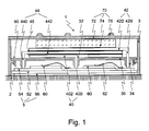
- FIG. 1 shows a section through an arrangement according to the invention of a power semiconductor module with a cooling component.
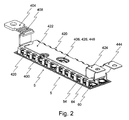
- Fig. 2 shows a three-dimensional view of a section through a second unit of an arrangement according to the invention.
- Fig. 1 shows a section through an arrangement of a power semiconductor module (1).
- This has a housing (3) with a frame-like housing part which is fixedly connected to the cooling member (2) of the arrangement.
- the frame-like housing part encloses the at least one substrate (5).
- This in turn has an insulating body (52), preferably an insulating ceramic, such as aluminum oxide or aluminum nitrite.
- the substrate (5) On the, the interior of the power semiconductor module (1) facing, the first main surface, the substrate (5) has a structured in itself Metallkaschtechnik.
- the individual sections of this metal lamination which is preferably configured as a copper lamination, form the printed conductors (54) of the power semiconductor module (1).
- the second main surface of the substrate (5) has a non-structured copper cladding (58) according to the prior art.
- controllable and / or uncontrolled power semiconductor devices such as IGBTs (insulated gate bipolar transistor) arranged in each case with antiparallel freewheeling diodes, or MOS-FETs. These are circuitally connected to other interconnects (54), for example by means of wire bonds (62) connected.
- the load connection elements (40, 42, 44) with the various necessary potentials serve for the external connection of the power electronic circuit inside the power semiconductor module (1).
- the load connection elements (40, 42, 44) are formed as metal moldings, each having a band-like portion (402, 422, 442) parallel to the substrate surface.
- the strip-like sections (402, 422, 442) in this case form a stack, wherein the band-like sections of the individual load connection elements (40, 42, 44) are spaced apart from one another exclusively by a necessary insulation, by way of example in the form of a plastic film (46). Necessary auxiliary connection elements are not shown for reasons of clarity in this sectional drawing.
- the power semiconductor module (1) preferably has an intermediate layer formed as an insulating molded body (30) between the stack of band-like sections (402, 422, 442) of the load connection elements (40, 42, 44) and the substrate (5).
- This Isolierstoffform Sciences (30) is arranged in this embodiment in the frame-like housing (3) by means of a snap-locking connection (90).
- the Isolierstoffformmaschine (30) in turn has recesses (32) for carrying out the contact feet (400, 420, 440) of the load connection elements (40, 42, 44). It is particularly preferred if these recesses (32) are designed as guides for these contact feet (400, 420, 440), whereby the positioning of the load connection elements (40, 42, 44) relative to the substrate (5) or its conductor tracks (54 ) is again improved over an arrangement with simple recesses. According to the invention, these recesses (32) have a width in any lateral direction, which is suitable for guiding the contact feet (400, 420, 440). on the other hand ensure their lateral movement up to at least 0.2mm, preferably up to 0.3mm.
- the pressure device (70) for the thermal connection of the power semiconductor module (1) with a cooling component (2) and at the same time for electrically contacting the load connection elements (40, 42, 44) with the conductor tracks (54) of the substrate (5) is formed by a pressure element ( 72) for pressure build-up and, an elastic cushion element as a pressure accumulator (74).
- the pressure is introduced via the cushion member (74) onto the stack of belt-like portions (402, 422, 442) of the load connection members (40, 42, 44) and thus exerts pressure on the contact pads (400, 420, 440). As a result, they are electrically connected to conductor tracks (54) of the substrate (5).
- Such pressure contacts (70) have proven over the life of power semiconductor modules (1) as particularly reliable contact. Also advantageous for the pressure contact is the formation of the recesses (32) of the Isolierstoffform stressess (32) as guides or shafts (34), as a result, the positioning of the contact feet (400, 420, 440) is particularly accurate.
- the pressure element (72) can be designed as a plastic molded body with a suitable inner metal core, which is designed as an example as a bimetal, and outer stiffening structures (76). It is further preferred if the pressure element (72) simultaneously serves as a cover of the power semiconductor module (1).
- the first unit of the arrangement is formed here by the cooling component (2), the housing (3) and the pressure element (72). The parts of this unit are firmly connected.
- the second unit is formed here from the substrate (5) with the circuit-connected power semiconductor components (60) and the load connection elements (40, 42, 44). The two units have no mechanically rigid connection to each other, but the second unit can move in each lateral direction at least 0.2mm, preferably 0.3mm, within the first unit.
- FIG. 2 shows a three-dimensional representation of a step through a second unit of an arrangement according to the invention.
- the latter has two substrates (5) with power semiconductor components (60, 64) arranged thereon and connected in a circuit-compatible manner by means of non-illustrated bond connections.
- the circuit shown is a half-bridge circuit having a plurality of parallel-connected bipolar transistors (60, 64) forming the respective first and second switches.
- the circuit also has the necessary freewheeling diodes (64).
- the first and second switches of the half-bridge circuit are in each case distributed in half to two identical substrates (5).
- the load connection elements (40, 42, 44) of this second unit of an arrangement according to the invention and their position relative to the substrates (5) are also shown. For reasons of clarity, the insulating plastic films between the individual load connection elements (40, 42, 44) are not shown.
- the load connection elements (40, 42, 44) have a plurality of contact feet (400, 420, 440) which extend from the associated band-like sections (402, 422, 442) of the respective load connection element (40, 42, 44).
- a plurality of contact feet (400, 420, 440) of the same polarity in this case contact the associated conductor tracks (54) of the respective polarity.
- the permanently contact-safe electrical connection is formed by means of the printing device (70) described above and not shown here.
- auxiliary connection elements Shown further are recess (406, 426, 446) of the stack of load connection elements (40, 42, 44), which are provided for the arrangement of the auxiliary connection elements. It is particularly preferred if all auxiliary connection elements are arranged centrally in the longitudinal direction of the power semiconductor module (1). Accordingly, it is advantageous if all auxiliary connection elements are arranged on a longitudinal section of the power semiconductor module which has at most half the length of the power semiconductor module (1). Furthermore, it is particularly preferred if the auxiliary connection elements are designed as coil springs.
- a mechanically flexible section (408) in the course of a load connection element, in this case the AC connection (40) of the power semiconductor module (1).
- This flexible portion (408) is disposed between the band-like portion (402) above the substrates (5) and an associated contactor (404) for external electrical connection of the assembly.
- this mechanically flexible portion (408) is here designed as copper mesh, as is known for flexible load current connections outside of a power semiconductor module.
- This copper mesh is weldably joined to the contactor (404) and a continuation of the ribbon-like portion (402).
- the lateral freedom of movement of the second unit of at least two tenths of a millimeter in the housing is achieved by means of suitable guided contact devices (424, 444) of the load connection elements shown here of the DC connections (42, 44).
Landscapes
- Engineering & Computer Science (AREA)
- Microelectronics & Electronic Packaging (AREA)
- Physics & Mathematics (AREA)
- Thermal Sciences (AREA)
- Cooling Or The Like Of Semiconductors Or Solid State Devices (AREA)
Abstract
Description
- Die Erfindung beschreibt eine Anordnung mit mindestens einem Leistungshalbleitermodul in Druckkontaktausführung und mit einem Kühlbauteil sowie ein zugehöriges Herstellungsverfahren. Einen Ausgangspunkt der Erfindung bilden Leistungshalbleitermodule wie sie beispielhaft aus der
DE 197 19 703 A1 bekannt sind. - Derartige Leistungshalbleitermodule bestehen nach dem Stand der Technik aus einem Gehäuse mit mindestens einem darin angeordneten elektrisch isolierenden Substrat vorzugsweise zur direkten Montage auf einem Kühlbauteil. Das Substrat seinerseits besteht aus einem Isolierstoffkörper mit einer Mehrzahl darauf befindlicher gegeneinander isolierter metallischer Verbindungsbahnen und hierauf befindlichen und mit diesen Verbindungsbahnen schaltungsgerecht verbundenen Leistungshalbleiterbauelementen. Weiterhin weisen die bekannten Leistungshalbleitermodule Anschlusselemente für externe Last- und Hilfsanschlüsse sowie im Inneren angeordnete Verbindungselemente auf. Diese Verbindungselemente für schaltungsgerechte Verbindungen im Inneren des Leistungshalbleitermoduls sind meist als Drahtbondverbindungen ausgebildet.
- Ebenfalls bekannt sind Druck kontaktierte Leistungshalbleitermodule, wie sie aus der
DE 42 37 632 A1 , derDE 199 03 875 A1 oder derDE 101 27 947 C1 bekannt sind. Bei erstgenannter Druckschrift weist die Druckeinrichtung ein stabiles, vorzugsweise metallisches, Druckelement zum Druckaufbau, ein elastisches Kissenelement zur Druck Speicherung und ein Brückenelement zur Druckeinleitung auf gesonderte Bereiche der Substratoberfläche auf. Das Brückenelement ist vorzugsweise ausgestaltet als ein Kunststoffformkörper mit einer dem Kissenelement zugewandten Fläche, von der eine Vielzahl von Druckfingern in Richtung der Substratoberfläche ausgeht. - Mittels einer derartigen Druckeinrichtung wird das Substrat auf ein Kühlbauteil gedrückt und somit der Wärmeübergang zwischen dem Substrat und dem Kühlbauteil dauerhaft sicher hergestellt. Das elastische Kissenelement dient hierbei der Aufrechterhaltung konstanter Druckverhältnisse bei unterschiedlichen thermischen Belastungen und über den gesamten Lebenszyklus des Leistungshalbleitermoduls.
- Die
DE 199 03 875 A1 bildet das bekannte Druckelement derart weiter, dass es einerseits ein besonders vorteilhaftes Verhältnis aus Gewicht und Stabilität aufweist und andererseits elektrisch isolierte Durchführungen aufweist. Hierzu ist das Druckelement als ein Kunststoffformkörper mit innen liegender Metallseele ausgebildet. Diese Metallseele weist Ausnehmungen für die Durchführung von Anschlusselementen, vorzugsweise Hilfsanschlusselementen in Federkontaktausführung, auf. Der Kunststoffformkörper umschließt diese Ausnehmungen derart, dass die Hilfsanschlusselemente mittels des Kunststoffformkörpers elektrisch von der Metallseele isoliert sind. - Es sind auch weitergebildete Druckelemente bekannt, die an ihrer dem Substrat zugewandten Oberfläche eine Vielzahl von Druckfingern aufweisen. Vorzugsweise weist hierbei die Metallseele noch eine voreingestellte Durchbiegung auf. In der Kombination beider Maßnahmen kann ein derartiges Druckelement die gesamte Funktionalität einer oben genannten Druckeinrichtung bereitstellen.
- Aus der
DE 101 57 947 C1 ist ein Leistungshalbleitermodul bekannt, wobei die Lastanschlusselemente derart ausgebildet sind, dass sie in Abschnitten eng benachbart senkrecht zur Substratoberfläche verlaufen und von dort ausgehende Kontaktfüße aufweisen, die den elektrischen Kontakt zu den Leiterbahnen herstellen und gleichzeitig Druck auf das Substrat ausüben und somit dessen thermischen Kontakt zu einem Kühlbauteil herstellen. Der Druck wird hierbei mit Mitteln nach dem Stand der Technik eingeleitet und gespeichert. - Aus der
DE 10 2004 021 927 A1 ist ein Verfahren zur inneren Isolation von Leistungshalbleitermodulen bekannt, wobei diese im Gegensatz zum vorbekannten Stand der Technik nicht bis zu einer definierten Füllhöhe mit einem isolierenden Silikongel verfüllt sind. Im Gegensatz dazu wird hier ein Verfahren zur Beschichtung der zu isolierenden Bauteile und Verbindungselemente vorgestellt, welches eine erhebliche Menge an Silikongel einspart. - Der Erfindung liegt die Aufgabe zugrunde eine Anordnung und ein zugehöriges Herstellungsverfahren für diese Anordnung mit mindestens einem Leistungshalbleitermodul in Druckkontaktausführung vorzustellen, wobei eine beliebige auch thermische Ausdehnungen des Substrats nicht auf das Gehäuse des Leistungshalbleitermoduls übertragen wird.
- Die Aufgabe wird erfindungsgemäß gelöst, durch die Maßnahmen der Merkmale der Ansprüche 1 und 7. Bevorzugte Ausführungsformen sind in den Unteransprüchen beschrieben.
- Der erfinderische Gedanke geht aus von einer Anordnung eines Leistungshalbleitermoduls in Druckkontaktausführung auf einem Kühlbauteil mit mindestens einem Substrat, mindestens zwei hierauf angeordneten steuerbaren Leistungshalbleiterbauelementen, beispielhaft bipolaren Transistoren, einem Gehäuse und nach außen führenden Last- und Steueranschlusselementen. Das Substrat selbst weist einen Isolierstoffkörper auf und auf dessen erster, dem Inneren des Leistungshalbleitermoduls zugewandten Hauptfläche Leiterbahnen mit Lastpotential. Weiterhin weist das Substrat vorzugsweise auch mindestens eine Leiterbahn mit Steuerpotential zu Ansteuerung der Leistungshalbleiterbauelemente auf.
- Das Leistungshalbleitermodul weist weiterhin Lastanschlusselemente jeweils ausgebildet als Metallformkörper mit einem bandartigen Abschnitt und mit einer Mehrzahl von diesem ausgehenden Kontaktfüßen auf. Die jeweiligen bandartige Abschnitte sind parallel zur Substratoberfläche und von dieser beabstandet angeordnet. Die Kontaktfüße, die von dem bandartigen Abschnitt ausgehen reichen zum Substrat und bilden dort schaltungsgerecht die Kontakte der Lastanschlüsse aus. Vorzugsweise kontaktieren sie hierzu auf dem Substrat die Leiterbahnen mit Lastpotential, alternativ auch direkt die Leistungshalbleiterbauelemente.
- Weiterhin kann zwischen den bandartigen Abschnitt der Lastanschlusselemente, die hierbei vorzugsweise einen Stapel ausbilden, und dem Substrat ein Isolierstoffformkörper angeordnet sein. Dieser Isolierstoffformkörper weist Ausnehmungen zur Durchführung der Kontaktfüße auf. Der Isolierstoffformkörper bildet hierbei vorzugsweise eine vollständig geschlossene Fläche aus, die ausschließlich Ausnehmungen für elektrische Anschlusselemente aufweist. Es kann weiterhin bevorzugt sein, wenn der Isolierstoffformkörper noch Ausnehmungen für Befestigungseinrichtungen des Leistungshalbleitermoduls auf dem Kühlbauteil aufweist.
- Das Gehäuse des Leistungshalbleitermoduls ist erfindungsgemäß fest mit dem Kühlbauteil verbunden. Ebenso ist die Druckplatte mechanisch fest mit dem Gehäuse verbunden. Somit bilden das Kühlbauteil, das Gehäuse und die Druckplatte eine erste Einheit der Anordnung aus. Das mindestens eine Substrat ist derart in dem rahmenartigen Gehäuse angeordnet, dass es sich beispielhaft durch thermische Einflüsse in engen Grenzen darin bewegen kann. Ebenso wenig weisen die Last- und Hilfsanschlusselemente starre Verbindungen mit dem Gehäuse auf. Diese können sich in allen Führungen gegenüber dem Gehäuse bewegen. Da die Druckeinleitung mittels des elastischen Druckspeichers erfolgt ist auch hier keine starre Verbindung gegeben. Somit ist die erste Einheit erfindungsgemäß von der zweiten Einheit gebildet aus dem mindestens einen Substrat und den Last- und Hilfsanschlusselementen mechanisch entkoppelt.
- Die Bewegungsfreiheit der zweiten innerhalb der ersten Einheit der erfinderischen Anordnung aus mindestens eine Leistungshalbleitermodul auf einem Kühlbauteil weist den wesentlichen Vorteil auf, dass beispielhaft durch thermische Einflüsse eingeprägte Bewegungen des Substrats nicht auf das Gehäuse des Leistungshalbleitermoduls übertragen werden.
- Das zugehörige Verfahren zur Herstellung einer oben genannten Anordnung weist die folgenden wesentlichen Schritte auf:
- Anordnen der Lastanschlusselemente mit geeigneter elektrischer Isolierung gegeneinander im Gehäuse des Leistungshalbleitermoduls.
- Anordnen des Druckspeichers oberhalb der Lastanschlusselemente.
- Vorläufige Arretierung der Druckplatte auf dem Druckspeicher an oder im Gehäuse.
- Anordnen mindestens eines mittels einer Isolierstoffmasse elektrisch isolierten Substrats mit hierauf angeordneten und schaltungsgerecht verbundenen Leistungshalbleiterbauelementen in einer zugeordneten Ausnehmung des Gehäuses, wobei die Isolierstoffmasse eine haftenden Verbindung zwischen dem Substrat und dem Gehäuse bildet.
- Anordnen mindestens eines Leistungshalbleitermoduls auf dem Kühlbauteil und Befestigung dessen Gehäuses auf dem Kühlbauteil.
- Druckeinleitung auf das Leistungshalbleitermodul über den Druckspeicher auf die Lastanschlusselemente und deren Kontaktfüße auf das mindestens eine Substrat zu dessen thermischen Kontaktierung mit dem Kühlbauteil durch Verschrauben der Druckplatte mit dem Gehäuse und / oder dem Kühlbauteil.
- Die Hilfsanschlusselemente werden zwischen zwei beliebigen Schritten vor Anordnung der Druckplatte in dafür vorgesehenen Führungen angeordnet. Weiterhin kann es besonders bevorzugt sein eine vorläufige Arretierung der Druckplatte auf dem Druckspeicher im Gehäuse mittels einer Schnapp- Rast- Verbindung zwischen der Druckplatte und dem Gehäuse auszuführen. Ebenso bevorzugt ist es die Isolierstoffmasse zuerst raupenartig um die Randbereiche des jeweiligen Substrats aufzubringen und anschließend den im Inneren der Raupe liegende Bereich zu vergießen.
- Die erfinderische Lösung wird an Hand der Ausführungsbeispiele der Fig. 1 und 2 weiter erläutert.
- Fig. 1 zeigt einen Schnitt durch eine erfindungsgemäße Anordnung eines Leistungshalbleitermoduls mit einem Kühlbauteil.
- Fig. 2 zeigt in dreidimensionaler Darstellung einen Schnitt durch eine zweite Einheit einer erfindungsgemäßen Anordnung.
- Fig. 1 zeigt einen Schnitt durch eine Anordnung eines Leistungshalbleitermoduls (1). Dieses weist ein Gehäuse (3) mit einen rahmenartigen Gehäuseteil auf, der fest mit dem Kühlbauteil (2) der Anordnung verbunden ist. Der rahmenartige Gehäuseteil umschließt hierbei das mindestens eine Substrat (5). Dieses wiederum weist einen Isolierstoffkörper (52), vorzugsweise eine Isolierkeramik, wie Aluminiumoxid oder Aluminiumnitrit auf.
- Auf der, dem Inneren des Leistungshalbleitermoduls (1) zugewandten, ersten Hauptfläche weist das Substrat (5) eine in sich strukturierte Metallkaschierung auf. Die einzelnen Abschnitte dieser vorzugsweise als Kupferkaschierung ausgestalteten Metallkaschierung bilden hierbei die Leiterbahnen (54) des Leistungshalbleitermoduls (1) aus. Die zweite Hauptfläche des Substrats (5) weist gemäß dem Stand der Technik eine nicht strukturierte Kupferkaschierung (58) auf.
- Auf den Leiterbahnen (54) des Substrats (5) sind steuerbare und / oder ungesteuerte Leistungshalbleiterbauelemente (60) wie beispielhaft IGBTs (insulated gate bipolar Transistor) mit jeweils antiparallel geschalteten Freilaufdioden, oder MOS-FETs angeordnet. Diese sind schaltungsgerecht mit weiteren Leiterbahnen (54), beispielhaft mittels Drahtbondverbindungen (62), verbunden.
- Die Lastanschlusselemente (40, 42, 44) mit den verschiedenen notwendigen Potentialen dienen der externen Verbindung der leistungselektronischen Schaltung im Inneren des Leistungshalbleitermoduls (1). Hierzu sind die Lastanschlusselemente (40, 42, 44) als Metallformkörper ausgebildet, die je einen bandartigen Abschnitt (402, 422, 442) parallel zur Substratoberfläche aufweisen. Die bandartigen Abschnitte (402, 422, 442) bilden hierbei einen Stapel, wobei die bandartigen Abschnitte der einzelnen Lastanschlusselemente (40, 42, 44) ausschließlich durch eine notwendige Isolierung, beispielhaft in Form einer Kunststofffolie (46), voneinander beabstandet sind. Notwendige Hilfsanschlusselemente sind aus Gründen der Übersichtlichkeit in dieser Schnittzeichnung nicht dargestellt.
- Vorzugsweise weist das erfindungsgemäße Leistungshalbleitermodul (1) eine als Isolierstoffformkörper (30) ausgebildete Zwischenlage zwischen dem Stapel der bandartigen Abschnitte (402, 422, 442) der Lastanschlusselemente (40, 42, 44) und dem Substrat (5) auf. Dieser Isolierstoffformkörper (30) ist in dieser Ausgestaltung in dem rahmenartigen Gehäuse (3) mittels einer Schnapp- Rast- Verbindung (90) angeordnet.
- Der Isolierstoffformkörper (30) weist seinerseits Ausnehmungen (32) zur Durchführung der Kontaktfüße (400, 420, 440) der Lastanschlusselemente (40, 42, 44) auf. Es ist besonders bevorzugt, wenn diese Ausnehmungen (32) als Führungen für diese Kontaktfüße (400, 420, 440) ausgebildet sind, wodurch die Positionierung der Lastanschlusselemente (40, 42, 44) relativ zum Substrat (5) bzw. dessen Leiterbahnen (54) nochmals gegenüber einer Anordnung mit einfachen Ausnehmungen verbessert wird. Erfindungsgemäß weisen diese Ausnehmungen (32) in jeglicher lateraler Richtung eine Breite auf, die geeignet ist eine Führung der Kontaktfüße (400, 420, 440) sicherzustellen und andererseits deren laterale Bewegung bis zu mindestens 0,2mm, vorzugsweise bis zu 0,3mm, zu gewährleisten.
- Die Druckeinrichtung (70) zur thermischen Verbindung des Leistungshalbleitermoduls (1) mit einem Kühlbauteil (2) und gleichzeitig zur elektrischen Kontaktierung der Lastanschlusselemente (40, 42, 44) mit den Leiterbahnen (54) des Substrats (5) wird gebildet durch ein Druckelement (72) zum Druckaufbau sowie, ein elastisches Kissenelement als Druckspeicher (74). Der Druck wird über das Kissenelement (74) auf den Stapel aus den bandartigen Abschnitten (402, 422, 442) der Lastanschlusselemente (40, 42, 44) eingeleitet und übt somit Druck auf die Kontaktfüße (400, 420, 440) aus. Hierdurch werden diese elektrisch leitend mit Leiterbahnen (54) des Substrats (5) verbunden.
- Derartige Druckkontaktierungen (70) haben sich über die Lebensdauer von Leistungshalbleitermodulen (1) als besonders kontaktsicher erwiesen. Weiterhin vorteilhaft für die Druckkontaktierung ist die Ausbildung der Ausnehmungen (32) des Isolierstoffformkörpers (32) als Führungen bzw. Schächte (34), da hierdurch die Positionierung der Kontaktfüße (400, 420, 440) besonders genau ist.
- Das Druckelement (72) kann gemäß dem Stand der Technik als Kunststoffformkörper mit geeigneter, beispielhaft als Bimetall ausgebildeter, innen liegender Metallseele und äußeren Versteifungsstrukturen (76) ausgeführt sein. Es ist weiterhin bevorzugt, wenn das Druckelement (72) gleichzeitig als Deckel des Leistungshalbleitermoduls (1) dient.
- Die erste Einheit der Anordnung wird hier gebildet durch das Kühlbauteil (2), das Gehäuse (3) und das Druckelement (72). Die Teile dieser Einheit sind fest miteinander verbundenen. Die zweite Einheit wird hier gebildet aus dem Substrat (5) mit den schaltungsgerecht verbundenen Leistungshalbleiterbauelementen (60) und den Lastanschlusselementen (40, 42, 44). Die beiden Einheiten weisen keine mechanisch starre Verbindung zueinander auf, vielmehr kann die zweite Einheit sich in jede laterale Richtung mindestens 0,2mm, vorzugsweise 0,3mm, innerhalb der ersten Einheit bewegen.
- Fig. 2 zeigt in dreidimensionaler Darstellung einen Schritt durch eine zweite Einheit einer erfindungsgemäßen Anordnung. Diese weist zwei Substrate (5) mit hierauf angeordneten und schaltungsgerecht mittels nicht dargestellter Bondverbindungen verbunden Leistungshalbleiterbauelementen (60, 64) auf. Die dargestellte Schaltung ist eine Halbbrückenschaltung mit einer Mehrzahl die jeweiligen ersten und zweiten Schalter bildenden parallel geschalteten bipolaren Transistoren (60, 64). Ebenfalls weist die Schaltung die notwendigen Freilaufdioden (64) auf. Die ersten und zweiten Schalter der Halbbrückenschaltung sind hierbei jeweils hälftig auf zwei identische Substrate (5) verteilt.
- Die Lastanschlusselemente (40, 42, 44) dieser zweiten Einheit einer erfindungsgemäßen Anordnung und deren Position zu den Substraten (5) ist ebenfalls dargestellt. Aus Gründen der Übersichtlichkeit sind die isolierenden Kunststofffolien zwischen den einzelnen Lastanschlusselementen (40, 42, 44) nicht dargestellt.
- Die Lastanschlusselemente (40, 42, 44) weisen eine Mehrzahl von Kontaktfüßen (400, 420, 440) auf, die von den zugeordneten bandartigen Abschnitten (402, 422, 442) des jeweiligen Lastanschlusselements (40, 42, 44) ausgehen. Jeweils eine Mehrzahl von Kontaktfüßen (400, 420, 440) gleicher Polarität kontaktieren hierbei die zugeordneten Leiterbahnen (54) der jeweiligen Polarität. Die dauerhaft kontaktsichere elektrische Verbindung wird mittels der oben beschriebenen und hier nicht dargestellten Druckeinrichtung (70) ausgebildet.
- Dargestellt sind weiterhin Ausnehmung (406, 426, 446) des Stapels aus Lastanschlusselementen (40, 42, 44), die vorgesehen sind für die Anordnung der Hilfsanschlusselemente. Es ist besonders bevorzugt, wenn alle Hilfsanschlusselemente in Längsrichtung des Leistungshalbleitermoduls (1) mittig angeordnet sind. Demgemäß ist es vorteilhaft, wenn alle Hilfsanschlusselemente auf einem Längsabschnitt des Leistungshalbleitermoduls angeordnet sind, der maximal die Halbe Länge des Leistungshalbleitermoduls (1) aufweist. Weiterhin ist es besonders bevorzugt, wenn die Hilfsanschlusselemente als Schraubenfedern ausgebildet sind.
- Weiterhin dargestellt ist ein mechanisch flexibler Abschnitt (408) im Verlauf eines Lastanschlusselements, hier des Wechselstromanschlusses (40) des Leistungshalbleitermoduls (1). Dieser flexible Abschnitt (408) ist angeordnet zwischen dem bandartigen Abschnitt (402) oberhalb der Substrate (5) und einer zugeordneten Kontakteinrichtung (404) zur externen elektrischen Verbindung der Anordnung.
- Die Ausbildung diese mechanisch flexiblen Abschnitts (408) ist hier als Kupfergewebe, ausgeführt, wie es für flexible Laststromverbindungen außerhalb eines Leistungshalbleitermoduls bekannt ist. Dieses Kupfergewebe ist mit der Kontakteinrichtung (404) und einer Fortsetzung des bandartigen Abschnitts (402) schweißtechnisch verbundenen.
- Alternative zu diesem flexiblen Abschnitt (408) wird die laterale Bewegungsfreiheit der zweiten Einheit von mindestens zwei Zehntel Millimeter im Gehäuse mittels geeignete geführter Kontakteinrichtungen (424, 444) der Lastanschlusselemente hier dargestellt der Gleichstromverbindungen (42, 44) erzielt.
Claims (9)
- Anordnung mindestens eines Leistungshalbleitermoduls (1) in Druckkontaktausführung auf einem Kühlbauteil (50), wobei das Leistungshalbleitermodul mindestens ein Substrat (5), mindestens zwei hierauf angeordnete Leistungshalbleiterbauelemente (60, 64), ein Gehäuse (3), nach außen führenden Last- (40, 42, 44) und Steueranschlusselementen und eine formstabilen Druckplatte (72) und einen elastischen Druckspeicher (74) aufweisenden Druckeinrichtung (70) aufweist,
wobei das Substrat (5) einen Isolierstoffkörper (52) aufweist und auf dessen erster dem Inneren des Leistungshalbleitermoduls (1) zugewandten Hauptfläche Leiterbahnen (54) mit Lastpotential angeordnet sind und
wobei die Lastanschlusselemente (40, 42, 44) jeweils als Metallformkörper mit einem bandartigen Abschnitt (402, 422, 442) und mit jeweils von diesem ausgehenden Kontaktfüßen (400, 420, 440) ausgebildet sind, der bandartige Abschnitt parallel zur Substratoberfläche und von dieser beabstandet angeordnet sind und die Kontaktfüße (400, 420, 440) von dem bandartigen Abschnitt (402, 422, 442) zu den Leiterbahnen (54) des Substrat (5) reichen und diese kontaktieren, und
wobei das Kühlbauteil (2), das Gehäuse (3) und die Druckplatte (72) eine erste Einheit bilden, die mechanisch entkoppelt ist von der zweiten Einheit gebildet aus Substrat (5) und Lastanschlusselementen (40, 42, 44). - Anordnung nach Anspruch 1
wobei Hilfsanschlusselemente in Längsrichtung des Leistungshalbleitermoduls (1) mittig angeordnet sind und der zugeordnete Längsabschnitt des Leistungshalbleitermoduls (1) maximal die Halbe Länge des Leistungshalbleitermoduls (1) aufweist. - Anordnung nach Anspruch 1,
wobei die Lastanschlusselemente (40, 42, 44) des Leistungshalbleitermoduls (1) zwischen dem bandartigen Abschnitt (402, 422, 442) oberhalb des Substrats (5) und einer jeweiligen Kontakteinrichtung (404, 424, 444) zur externen Verbindung einen mechanisch flexiblen Abschnitt (408) aufweisen. - Anordnung nach Anspruch 3,
wobei der mechanisch flexible Abschnitt (40) als Kupfergewebe ausgebildet ist. - Anordnung nach Anspruch 4,
wobei das Kupfergewebe schweißtechnisch mit dem zugeordneten Lastanschlusselement (40, 42, 44) verbundenen ist. - Anordnung nach einem der vorgenannten Ansprüche,
wobei das jeweilige Substrat (5) eine laterale Bewegungsfreiheit von mindestens zwei Zehntel Millimeter im Gehäuse (3) aufweist. - Verfahren zur Herstellung einer Anordnung nach Anspruch 1 gekennzeichnet durch folgende Schritte:• Anordnen der Lastanschlusselemente (40, 42, 44) mit geeigneter elektrischer Isolierung (46) gegeneinander im Gehäuse (3) des Leistungshalbleitermoduls (1);• Anordnen des Druckspeichers (74) oberhalb der Lastanschlusselemente (40, 42, 44);• Vorläufige Arretierung der Druckplatte (72) auf dem Druckspeicher (74) an oder im Gehäuse (3);• Anordnen mindestens eines mittels einer Isolierstoffmasse elektrisch isolierten Substrats (5) mit hierauf angeordneten und schaltungsgerecht verbundenen Leistungshalbleiterbauelementen (60, 64) in der Ausnehmung des Gehäuses (3),wobei die Isolierstoffmasse eine haftenden Verbindung zwischen dem Substrat (5) und dem Gehäuse (3) bildet;• Anordnen mindestens eines Leistungshalbleitermoduls (1) auf dem Kühlbauteil (2) und Befestigung des Gehäuses (3)auf dem Kühlbauteil (1);• Druckeinleitung auf das Leistungshalbleitermodul (1) über die Druckplatte (72) und den Druckspeicher (74) auf die Lastanschlusselemente (40, 42, 44) und deren Kontaktfüße (400, 420, 440) auf das mindestens eine Substrat (5) zu dessen thermischer Kontaktierung mit dem Kühlbauteil (2) durch Verschrauben der Druckplatte (72) mit dem Gehäuse (3) und / oder dem Kühlbauteil (2);Die Hilfsanschlusselemente werden zwischen zwei beliebigen Schritten vor Anordnung der Druckplatte (72) in dafür vorgesehenen Führungen angeordnet.
- Verfahren nach Anspruch 7
wobei die vorläufige Arretierung der Druckplatte (72) auf dem Druckspeicher (74) im Gehäuse (3) mittels einer Schnapp- Rast- Verbindung zwischen der Druckplatte (72) und dem Gehäuse (3) erfolgt. - Verfahren nach Anspruch 7
wobei die Isolierstoffmasse zuerst raupenartig um die Randbereiche des Substrats (5) aufgebracht wird und anschließend der im Inneren der Raupe liegende Bereich vergossen wird.
Applications Claiming Priority (1)
| Application Number | Priority Date | Filing Date | Title |
|---|---|---|---|
| DE102006006424A DE102006006424B4 (de) | 2006-02-13 | 2006-02-13 | Anordnung mit mindestens einem Leistungshalbleitermodul und einem Kühlbauteil und zugehöriges Herstellungsverfahren |
Publications (3)
| Publication Number | Publication Date |
|---|---|
| EP1818982A2 true EP1818982A2 (de) | 2007-08-15 |
| EP1818982A3 EP1818982A3 (de) | 2010-11-10 |
| EP1818982B1 EP1818982B1 (de) | 2014-01-01 |
Family
ID=37966749
Family Applications (1)
| Application Number | Title | Priority Date | Filing Date |
|---|---|---|---|
| EP07002032.6A Not-in-force EP1818982B1 (de) | 2006-02-13 | 2007-01-31 | Anordnung mit mindestens einem Leistungshalbleitermodul und einem Kühlbauteil und zugehöriges Herstellungsverfahren |
Country Status (4)
| Country | Link |
|---|---|
| US (1) | US7592698B2 (de) |
| EP (1) | EP1818982B1 (de) |
| JP (1) | JP5114065B2 (de) |
| DE (1) | DE102006006424B4 (de) |
Cited By (5)
| Publication number | Priority date | Publication date | Assignee | Title |
|---|---|---|---|---|
| DE102007003587A1 (de) * | 2007-01-24 | 2008-08-07 | Semikron Elektronik Gmbh & Co. Kg | Leistungshalbleitermodul mit Druckkörper |
| EP2211384A3 (de) * | 2009-01-23 | 2010-11-03 | SEMIKRON Elektronik GmbH & Co. KG | Leistungshalbleitermodul in Druckkontaktausführung mit aktiver Kühleinrichtung |
| EP2330623A1 (de) * | 2009-12-05 | 2011-06-08 | SEMIKRON Elektronik GmbH & Co. KG | Druckkontaktiertes Leistungshalbleitermodul mit teilweise bandartigen Lastanschlusselementen |
| CN103367279B (zh) * | 2012-03-30 | 2017-05-03 | 南京皓赛米电力科技有限公司 | 双面微通道液冷功率半导体整晶圆平板压接封装结构 |
| CN107026136A (zh) * | 2016-02-01 | 2017-08-08 | 赛米控电子股份有限公司 | 具有压力施加体的功率半导体模块及其布置 |
Families Citing this family (16)
| Publication number | Priority date | Publication date | Assignee | Title |
|---|---|---|---|---|
| DE102006006423B4 (de) * | 2006-02-13 | 2009-06-10 | Semikron Elektronik Gmbh & Co. Kg | Leistungshalbleitermodul und zugehöriges Herstellungsverfahren |
| DE102006006425B4 (de) * | 2006-02-13 | 2009-06-10 | Semikron Elektronik Gmbh & Co. Kg | Leistungshalbleitermodul in Druckkontaktausführung |
| DE102006052620B4 (de) * | 2006-11-08 | 2009-07-09 | Semikron Elektronik Gmbh & Co. Kg | Schaltungsanordnung mit einem Leistungsmodul, das mit einer Leiterplatte kombiniert ist. |
| DE102007045261A1 (de) * | 2007-09-21 | 2009-04-23 | Continental Automotive Gmbh | Elektrisches Gerät, insbesondere Steuergerät für ein Kraftfahrzeug |
| DE102007054709B4 (de) * | 2007-11-16 | 2014-11-13 | Semikron Elektronik Gmbh & Co. Kg | Leistungshalbleitermodul mit einem Substrat und mit einer Druckeinrichtung |
| DE102008034068B4 (de) | 2008-07-22 | 2019-07-18 | Semikron Elektronik Gmbh & Co. Kg | Leistungshalbleitermodul |
| KR101073286B1 (ko) * | 2008-12-03 | 2011-10-12 | 엘에스산전 주식회사 | 전력용 반도체 모듈 |
| DE102009046403B4 (de) * | 2009-11-04 | 2015-05-28 | Semikron Elektronik Gmbh & Co. Kg | Leistungshalbleitermodul in Druckkontakttechnik |
| DE102009057146B4 (de) * | 2009-12-05 | 2013-09-26 | Semikron Elektronik Gmbh & Co. Kg | Druckkontaktiertes Leistungshalbleitermodul mit Hybriddruckspeicher |
| DE102013200526B4 (de) | 2013-01-16 | 2019-11-21 | Semikron Elektronik Gmbh & Co. Kg | Leistungshalbleitermodul und Verfahren zur Herstellung eines Leistungshalbleitermoduls |
| DE102013104950B3 (de) * | 2013-05-14 | 2014-04-30 | Semikron Elektronik Gmbh & Co. Kg | Leistungshalbleitermodul und Anordnung hiermit |
| US9431311B1 (en) | 2015-02-19 | 2016-08-30 | Semiconductor Components Industries, Llc | Semiconductor package with elastic coupler and related methods |
| DE102015109710B4 (de) * | 2015-06-17 | 2019-10-31 | Avl Software And Functions Gmbh | Design einer Leistungszelle |
| DE102016113152B4 (de) * | 2016-07-18 | 2019-12-19 | Semikron Elektronik Gmbh & Co. Kg | Leistungselektronische Schalteinrichtung und Leistungshalbleitermodul hiermit |
| DE102017129707B4 (de) * | 2017-12-13 | 2024-12-12 | Semikron Elektronik Gmbh & Co. Kg | Verfahren zur Herstellung eines leistungselektronischen Systems |
| DE102018129336B4 (de) | 2018-11-21 | 2021-07-08 | Semikron Elektronik Gmbh & Co. Kg | Leistungshalbleitermodul mit einem Substrat und mit einem Lastanschlusselement |
Family Cites Families (16)
| Publication number | Priority date | Publication date | Assignee | Title |
|---|---|---|---|---|
| DE2942409A1 (de) * | 1979-10-19 | 1981-04-23 | Siemens AG, 1000 Berlin und 8000 München | Halbleiterbauelement mit mehreren halbleiterkoerpern |
| DE3643288A1 (de) * | 1986-12-18 | 1988-06-30 | Semikron Elektronik Gmbh | Halbleiterbaueinheit |
| US5345107A (en) * | 1989-09-25 | 1994-09-06 | Hitachi, Ltd. | Cooling apparatus for electronic device |
| DE4237632A1 (de) * | 1992-11-07 | 1994-05-11 | Export Contor Ausenhandelsgese | Schaltungsanordnung |
| JP3396566B2 (ja) * | 1995-10-25 | 2003-04-14 | 三菱電機株式会社 | 半導体装置 |
| DE19617055C1 (de) * | 1996-04-29 | 1997-06-26 | Semikron Elektronik Gmbh | Halbleiterleistungsmodul hoher Packungsdichte in Mehrschichtbauweise |
| DE19719703C5 (de) * | 1997-05-09 | 2005-11-17 | eupec Europäische Gesellschaft für Leistungshalbleiter mbH & Co. KG | Leistungshalbleitermodul mit Keramiksubstrat |
| JPH113995A (ja) * | 1997-06-12 | 1999-01-06 | Toshiba Corp | 半導体装置 |
| JPH11330283A (ja) * | 1998-05-15 | 1999-11-30 | Toshiba Corp | 半導体モジュール及び大型半導体モジュール |
| DE19903875C2 (de) * | 1999-02-01 | 2001-11-29 | Semikron Elektronik Gmbh | Leistungshalbleiterschaltungsanordnung, insbesondere Stromumrichter, in Druckkontaktierung |
| US6703707B1 (en) * | 1999-11-24 | 2004-03-09 | Denso Corporation | Semiconductor device having radiation structure |
| DE10121970B4 (de) * | 2001-05-05 | 2004-05-27 | Semikron Elektronik Gmbh | Leistungshalbleitermodul in Druckkontaktierung |
| DE10127947C1 (de) * | 2001-08-22 | 2002-10-17 | Semikron Elektronik Gmbh | Schaltungsanordnung |
| DE102004021927B4 (de) * | 2004-05-04 | 2008-07-03 | Semikron Elektronik Gmbh & Co. Kg | Verfahren zur inneren elektrischen Isolation eines Substrats für ein Leistungshalbleitermodul |
| DE102006006425B4 (de) * | 2006-02-13 | 2009-06-10 | Semikron Elektronik Gmbh & Co. Kg | Leistungshalbleitermodul in Druckkontaktausführung |
| DE102006006423B4 (de) * | 2006-02-13 | 2009-06-10 | Semikron Elektronik Gmbh & Co. Kg | Leistungshalbleitermodul und zugehöriges Herstellungsverfahren |
-
2006
- 2006-02-13 DE DE102006006424A patent/DE102006006424B4/de not_active Expired - Fee Related
-
2007
- 2007-01-31 EP EP07002032.6A patent/EP1818982B1/de not_active Not-in-force
- 2007-02-09 JP JP2007030496A patent/JP5114065B2/ja not_active Expired - Fee Related
- 2007-02-13 US US11/705,729 patent/US7592698B2/en not_active Expired - Fee Related
Cited By (7)
| Publication number | Priority date | Publication date | Assignee | Title |
|---|---|---|---|---|
| DE102007003587A1 (de) * | 2007-01-24 | 2008-08-07 | Semikron Elektronik Gmbh & Co. Kg | Leistungshalbleitermodul mit Druckkörper |
| DE102007003587B4 (de) * | 2007-01-24 | 2009-06-10 | Semikron Elektronik Gmbh & Co. Kg | Leistungshalbleitermodul mit Druckkörper |
| EP2211384A3 (de) * | 2009-01-23 | 2010-11-03 | SEMIKRON Elektronik GmbH & Co. KG | Leistungshalbleitermodul in Druckkontaktausführung mit aktiver Kühleinrichtung |
| EP2330623A1 (de) * | 2009-12-05 | 2011-06-08 | SEMIKRON Elektronik GmbH & Co. KG | Druckkontaktiertes Leistungshalbleitermodul mit teilweise bandartigen Lastanschlusselementen |
| CN103367279B (zh) * | 2012-03-30 | 2017-05-03 | 南京皓赛米电力科技有限公司 | 双面微通道液冷功率半导体整晶圆平板压接封装结构 |
| CN107026136A (zh) * | 2016-02-01 | 2017-08-08 | 赛米控电子股份有限公司 | 具有压力施加体的功率半导体模块及其布置 |
| CN107026136B (zh) * | 2016-02-01 | 2022-02-22 | 赛米控电子股份有限公司 | 具有压力施加体的功率半导体模块及其布置 |
Also Published As
| Publication number | Publication date |
|---|---|
| US7592698B2 (en) | 2009-09-22 |
| US20070194443A1 (en) | 2007-08-23 |
| JP2007221128A (ja) | 2007-08-30 |
| JP5114065B2 (ja) | 2013-01-09 |
| DE102006006424A1 (de) | 2007-08-23 |
| DE102006006424B4 (de) | 2011-11-17 |
| EP1818982A3 (de) | 2010-11-10 |
| EP1818982B1 (de) | 2014-01-01 |
Similar Documents
| Publication | Publication Date | Title |
|---|---|---|
| EP1818982B1 (de) | Anordnung mit mindestens einem Leistungshalbleitermodul und einem Kühlbauteil und zugehöriges Herstellungsverfahren | |
| EP1843393B1 (de) | Leistungshalbleitermodul in Druckkontaktausführung | |
| EP1830404B1 (de) | Leistungshalbleitermodul | |
| EP1868243B1 (de) | Leistungshalbleitermodul mit gegeneinander elektrisch isolierten Anschlusselementen | |
| DE102017109706B3 (de) | Leistungselektronische Anordnung mit Gleichspannungsverbindungselement | |
| DE102009037257B4 (de) | Leistungshalbleitermodul mit Schaltungsträger und Lastanschlusselement sowie Herstellungsverfahren hierzu | |
| DE102015214457A1 (de) | Ansteuereinheit mit anschlüssen in federndem kontakt miteinander | |
| DE102017115883A1 (de) | Leistungselektronisches Submodul mit Gleich- und Wechselspannungsanschlusselementen und Anordnung hiermit | |
| EP4099555B1 (de) | Halbbrücke für einen elektrischen antrieb eines elektrofahrzeugs oder eines hybridfahrzeugs, leistungsmodul für einen inverter und inverter | |
| DE10340297B4 (de) | Verbindugsanordnung zur Verbindung von aktiven und passiven elektrischen und elektronischen Bauelementen | |
| EP2548423A1 (de) | Schaltungsanordnung und zugehöriges steuergerät für ein kraftfahrzeug | |
| DE102005055713B4 (de) | Leistungshalbleitermodul mit Anschlusselementen | |
| EP1950807B1 (de) | Leistungshalbleitermodul mit Druckkörper | |
| EP2548424B1 (de) | Schaltungsanordnung und zugehöriges steuergerät für ein kraftfahrzeug | |
| EP2003693B1 (de) | Druckkontaktiertes dreiphasiges Stromrichtermodul | |
| DE102006032436A1 (de) | Vorrichtung zur Anordnung an einer Leiterplatte | |
| DE102021203704A1 (de) | Halbbrücke, Leistungsmodul und Inverter für einen elektrischen Antrieb eines Elektrofahrzeugs oder eines Hybridfahrzeugs | |
| DE102013215648A1 (de) | Leistungselektronikmodul mit Substrat, Bauelement und Leiterplatte | |
| DE102008014113B4 (de) | Leistungshalbleitermodul in Druckkontaktausführung | |
| DE102021113502A1 (de) | Elektronische Baugruppe mit Platinenverbinder, Elektronikmodul sowie Kraftfahrzeug | |
| EP2110853A2 (de) | Anordnung in Druckkontaktausführung mit einem Leistungshalbleitermodul | |
| WO2015086814A1 (de) | Verfahren zum herstellen einer baugruppe und baugruppe |
Legal Events
| Date | Code | Title | Description |
|---|---|---|---|
| PUAI | Public reference made under article 153(3) epc to a published international application that has entered the european phase |
Free format text: ORIGINAL CODE: 0009012 |
|
| AK | Designated contracting states |
Kind code of ref document: A2 Designated state(s): AT BE BG CH CY CZ DE DK EE ES FI FR GB GR HU IE IS IT LI LT LU LV MC NL PL PT RO SE SI SK TR |
|
| AX | Request for extension of the european patent |
Extension state: AL BA HR MK YU |
|
| PUAL | Search report despatched |
Free format text: ORIGINAL CODE: 0009013 |
|
| AK | Designated contracting states |
Kind code of ref document: A3 Designated state(s): AT BE BG CH CY CZ DE DK EE ES FI FR GB GR HU IE IS IT LI LT LU LV MC NL PL PT RO SE SI SK TR |
|
| AX | Request for extension of the european patent |
Extension state: AL BA HR MK RS |
|
| 17P | Request for examination filed |
Effective date: 20101021 |
|
| RIC1 | Information provided on ipc code assigned before grant |
Ipc: H01L 23/48 20060101AFI20101116BHEP |
|
| AKX | Designation fees paid |
Designated state(s): AT BE BG CH CY CZ DE DK EE ES FI FR GB GR HU IE IS IT LI LT LU LV MC NL PL PT RO SE SI SK TR |
|
| GRAJ | Information related to disapproval of communication of intention to grant by the applicant or resumption of examination proceedings by the epo deleted |
Free format text: ORIGINAL CODE: EPIDOSDIGR1 |
|
| GRAP | Despatch of communication of intention to grant a patent |
Free format text: ORIGINAL CODE: EPIDOSNIGR1 |
|
| GRAP | Despatch of communication of intention to grant a patent |
Free format text: ORIGINAL CODE: EPIDOSNIGR1 |
|
| INTG | Intention to grant announced |
Effective date: 20130606 |
|
| INTG | Intention to grant announced |
Effective date: 20130613 |
|
| GRAS | Grant fee paid |
Free format text: ORIGINAL CODE: EPIDOSNIGR3 |
|
| GRAA | (expected) grant |
Free format text: ORIGINAL CODE: 0009210 |
|
| AK | Designated contracting states |
Kind code of ref document: B1 Designated state(s): AT BE BG CH CY CZ DE DK EE ES FI FR GB GR HU IE IS IT LI LT LU LV MC NL PL PT RO SE SI SK TR |
|
| REG | Reference to a national code |
Ref country code: GB Ref legal event code: FG4D Free format text: NOT ENGLISH |
|
| REG | Reference to a national code |
Ref country code: CH Ref legal event code: EP |
|
| REG | Reference to a national code |
Ref country code: IE Ref legal event code: FG4D Free format text: LANGUAGE OF EP DOCUMENT: GERMAN |
|
| REG | Reference to a national code |
Ref country code: DE Ref legal event code: R096 Ref document number: 502007012650 Country of ref document: DE Effective date: 20140213 |
|
| REG | Reference to a national code |
Ref country code: AT Ref legal event code: REF Ref document number: 647920 Country of ref document: AT Kind code of ref document: T Effective date: 20140215 |
|
| REG | Reference to a national code |
Ref country code: NL Ref legal event code: VDEP Effective date: 20140101 |
|
| REG | Reference to a national code |
Ref country code: LT Ref legal event code: MG4D |
|
| BERE | Be: lapsed |
Owner name: SEMIKRON ELEKTRONIK G.M.B.H. & CO. KG Effective date: 20140131 |
|
| PG25 | Lapsed in a contracting state [announced via postgrant information from national office to epo] |
Ref country code: LT Free format text: LAPSE BECAUSE OF FAILURE TO SUBMIT A TRANSLATION OF THE DESCRIPTION OR TO PAY THE FEE WITHIN THE PRESCRIBED TIME-LIMIT Effective date: 20140101 Ref country code: IS Free format text: LAPSE BECAUSE OF FAILURE TO SUBMIT A TRANSLATION OF THE DESCRIPTION OR TO PAY THE FEE WITHIN THE PRESCRIBED TIME-LIMIT Effective date: 20140501 |
|
| PG25 | Lapsed in a contracting state [announced via postgrant information from national office to epo] |
Ref country code: FI Free format text: LAPSE BECAUSE OF FAILURE TO SUBMIT A TRANSLATION OF THE DESCRIPTION OR TO PAY THE FEE WITHIN THE PRESCRIBED TIME-LIMIT Effective date: 20140101 Ref country code: CY Free format text: LAPSE BECAUSE OF FAILURE TO SUBMIT A TRANSLATION OF THE DESCRIPTION OR TO PAY THE FEE WITHIN THE PRESCRIBED TIME-LIMIT Effective date: 20140101 Ref country code: PT Free format text: LAPSE BECAUSE OF FAILURE TO SUBMIT A TRANSLATION OF THE DESCRIPTION OR TO PAY THE FEE WITHIN THE PRESCRIBED TIME-LIMIT Effective date: 20140502 Ref country code: NL Free format text: LAPSE BECAUSE OF FAILURE TO SUBMIT A TRANSLATION OF THE DESCRIPTION OR TO PAY THE FEE WITHIN THE PRESCRIBED TIME-LIMIT Effective date: 20140101 Ref country code: ES Free format text: LAPSE BECAUSE OF FAILURE TO SUBMIT A TRANSLATION OF THE DESCRIPTION OR TO PAY THE FEE WITHIN THE PRESCRIBED TIME-LIMIT Effective date: 20140101 Ref country code: SE Free format text: LAPSE BECAUSE OF FAILURE TO SUBMIT A TRANSLATION OF THE DESCRIPTION OR TO PAY THE FEE WITHIN THE PRESCRIBED TIME-LIMIT Effective date: 20140101 |
|
| REG | Reference to a national code |
Ref country code: CH Ref legal event code: PL |
|
| PG25 | Lapsed in a contracting state [announced via postgrant information from national office to epo] |
Ref country code: LV Free format text: LAPSE BECAUSE OF FAILURE TO SUBMIT A TRANSLATION OF THE DESCRIPTION OR TO PAY THE FEE WITHIN THE PRESCRIBED TIME-LIMIT Effective date: 20140101 |
|
| REG | Reference to a national code |
Ref country code: DE Ref legal event code: R097 Ref document number: 502007012650 Country of ref document: DE |
|
| PG25 | Lapsed in a contracting state [announced via postgrant information from national office to epo] |
Ref country code: MC Free format text: LAPSE BECAUSE OF FAILURE TO SUBMIT A TRANSLATION OF THE DESCRIPTION OR TO PAY THE FEE WITHIN THE PRESCRIBED TIME-LIMIT Effective date: 20140101 Ref country code: CZ Free format text: LAPSE BECAUSE OF FAILURE TO SUBMIT A TRANSLATION OF THE DESCRIPTION OR TO PAY THE FEE WITHIN THE PRESCRIBED TIME-LIMIT Effective date: 20140101 Ref country code: DK Free format text: LAPSE BECAUSE OF FAILURE TO SUBMIT A TRANSLATION OF THE DESCRIPTION OR TO PAY THE FEE WITHIN THE PRESCRIBED TIME-LIMIT Effective date: 20140101 Ref country code: EE Free format text: LAPSE BECAUSE OF FAILURE TO SUBMIT A TRANSLATION OF THE DESCRIPTION OR TO PAY THE FEE WITHIN THE PRESCRIBED TIME-LIMIT Effective date: 20140101 Ref country code: CH Free format text: LAPSE BECAUSE OF NON-PAYMENT OF DUE FEES Effective date: 20140131 Ref country code: RO Free format text: LAPSE BECAUSE OF FAILURE TO SUBMIT A TRANSLATION OF THE DESCRIPTION OR TO PAY THE FEE WITHIN THE PRESCRIBED TIME-LIMIT Effective date: 20140101 Ref country code: LI Free format text: LAPSE BECAUSE OF NON-PAYMENT OF DUE FEES Effective date: 20140131 |
|
| REG | Reference to a national code |
Ref country code: IE Ref legal event code: MM4A |
|
| PLBE | No opposition filed within time limit |
Free format text: ORIGINAL CODE: 0009261 |
|
| STAA | Information on the status of an ep patent application or granted ep patent |
Free format text: STATUS: NO OPPOSITION FILED WITHIN TIME LIMIT |
|
| PG25 | Lapsed in a contracting state [announced via postgrant information from national office to epo] |
Ref country code: SK Free format text: LAPSE BECAUSE OF FAILURE TO SUBMIT A TRANSLATION OF THE DESCRIPTION OR TO PAY THE FEE WITHIN THE PRESCRIBED TIME-LIMIT Effective date: 20140101 Ref country code: PL Free format text: LAPSE BECAUSE OF FAILURE TO SUBMIT A TRANSLATION OF THE DESCRIPTION OR TO PAY THE FEE WITHIN THE PRESCRIBED TIME-LIMIT Effective date: 20140101 |
|
| 26N | No opposition filed |
Effective date: 20141002 |
|
| REG | Reference to a national code |
Ref country code: DE Ref legal event code: R097 Ref document number: 502007012650 Country of ref document: DE Effective date: 20141002 |
|
| PG25 | Lapsed in a contracting state [announced via postgrant information from national office to epo] |
Ref country code: BE Free format text: LAPSE BECAUSE OF NON-PAYMENT OF DUE FEES Effective date: 20140131 Ref country code: IE Free format text: LAPSE BECAUSE OF NON-PAYMENT OF DUE FEES Effective date: 20140131 |
|
| REG | Reference to a national code |
Ref country code: AT Ref legal event code: MM01 Ref document number: 647920 Country of ref document: AT Kind code of ref document: T Effective date: 20140131 |
|
| PG25 | Lapsed in a contracting state [announced via postgrant information from national office to epo] |
Ref country code: SI Free format text: LAPSE BECAUSE OF FAILURE TO SUBMIT A TRANSLATION OF THE DESCRIPTION OR TO PAY THE FEE WITHIN THE PRESCRIBED TIME-LIMIT Effective date: 20140101 Ref country code: AT Free format text: LAPSE BECAUSE OF NON-PAYMENT OF DUE FEES Effective date: 20140131 |
|
| REG | Reference to a national code |
Ref country code: FR Ref legal event code: PLFP Year of fee payment: 10 |
|
| PG25 | Lapsed in a contracting state [announced via postgrant information from national office to epo] |
Ref country code: BG Free format text: LAPSE BECAUSE OF FAILURE TO SUBMIT A TRANSLATION OF THE DESCRIPTION OR TO PAY THE FEE WITHIN THE PRESCRIBED TIME-LIMIT Effective date: 20140101 |
|
| PG25 | Lapsed in a contracting state [announced via postgrant information from national office to epo] |
Ref country code: IT Free format text: LAPSE BECAUSE OF FAILURE TO SUBMIT A TRANSLATION OF THE DESCRIPTION OR TO PAY THE FEE WITHIN THE PRESCRIBED TIME-LIMIT Effective date: 20140101 Ref country code: GR Free format text: LAPSE BECAUSE OF FAILURE TO SUBMIT A TRANSLATION OF THE DESCRIPTION OR TO PAY THE FEE WITHIN THE PRESCRIBED TIME-LIMIT Effective date: 20140402 |
|
| PG25 | Lapsed in a contracting state [announced via postgrant information from national office to epo] |
Ref country code: HU Free format text: LAPSE BECAUSE OF FAILURE TO SUBMIT A TRANSLATION OF THE DESCRIPTION OR TO PAY THE FEE WITHIN THE PRESCRIBED TIME-LIMIT; INVALID AB INITIO Effective date: 20070131 Ref country code: TR Free format text: LAPSE BECAUSE OF FAILURE TO SUBMIT A TRANSLATION OF THE DESCRIPTION OR TO PAY THE FEE WITHIN THE PRESCRIBED TIME-LIMIT Effective date: 20140101 Ref country code: LU Free format text: LAPSE BECAUSE OF NON-PAYMENT OF DUE FEES Effective date: 20140131 |
|
| REG | Reference to a national code |
Ref country code: FR Ref legal event code: PLFP Year of fee payment: 11 |
|
| REG | Reference to a national code |
Ref country code: FR Ref legal event code: PLFP Year of fee payment: 12 |
|
| PGFP | Annual fee paid to national office [announced via postgrant information from national office to epo] |
Ref country code: GB Payment date: 20190206 Year of fee payment: 13 Ref country code: GB Payment date: 20190124 Year of fee payment: 13 |
|
| GBPC | Gb: european patent ceased through non-payment of renewal fee |
Effective date: 20200131 |
|
| PG25 | Lapsed in a contracting state [announced via postgrant information from national office to epo] |
Ref country code: FR Free format text: LAPSE BECAUSE OF NON-PAYMENT OF DUE FEES Effective date: 20200131 Ref country code: GB Free format text: LAPSE BECAUSE OF NON-PAYMENT OF DUE FEES Effective date: 20200131 |
|
| PGFP | Annual fee paid to national office [announced via postgrant information from national office to epo] |
Ref country code: DE Payment date: 20240131 Year of fee payment: 18 |
|
| REG | Reference to a national code |
Ref country code: DE Ref legal event code: R119 Ref document number: 502007012650 Country of ref document: DE |
|
| PG25 | Lapsed in a contracting state [announced via postgrant information from national office to epo] |
Ref country code: DE Free format text: LAPSE BECAUSE OF NON-PAYMENT OF DUE FEES Effective date: 20250801 |