EP1818982A2 - Assemblage avec au moins une module de semi-conducteur à haut prestation et un élément de refroidissement et méthode de fabrication associée - Google Patents
Assemblage avec au moins une module de semi-conducteur à haut prestation et un élément de refroidissement et méthode de fabrication associée Download PDFInfo
- Publication number
- EP1818982A2 EP1818982A2 EP07002032A EP07002032A EP1818982A2 EP 1818982 A2 EP1818982 A2 EP 1818982A2 EP 07002032 A EP07002032 A EP 07002032A EP 07002032 A EP07002032 A EP 07002032A EP 1818982 A2 EP1818982 A2 EP 1818982A2
- Authority
- EP
- European Patent Office
- Prior art keywords
- power semiconductor
- substrate
- semiconductor module
- housing
- connection elements
- Prior art date
- Legal status (The legal status is an assumption and is not a legal conclusion. Google has not performed a legal analysis and makes no representation as to the accuracy of the status listed.)
- Granted
Links
Images
Classifications
-
- H—ELECTRICITY
- H05—ELECTRIC TECHNIQUES NOT OTHERWISE PROVIDED FOR
- H05K—PRINTED CIRCUITS; CASINGS OR CONSTRUCTIONAL DETAILS OF ELECTRIC APPARATUS; MANUFACTURE OF ASSEMBLAGES OF ELECTRICAL COMPONENTS
- H05K7/00—Constructional details common to different types of electric apparatus
- H05K7/20—Modifications to facilitate cooling, ventilating, or heating
- H05K7/2039—Modifications to facilitate cooling, ventilating, or heating characterised by the heat transfer by conduction from the heat generating element to a dissipating body
- H05K7/20436—Inner thermal coupling elements in heat dissipating housings, e.g. protrusions or depressions integrally formed in the housing
- H05K7/2049—Pressing means used to urge contact, e.g. springs
-
- H—ELECTRICITY
- H05—ELECTRIC TECHNIQUES NOT OTHERWISE PROVIDED FOR
- H05K—PRINTED CIRCUITS; CASINGS OR CONSTRUCTIONAL DETAILS OF ELECTRIC APPARATUS; MANUFACTURE OF ASSEMBLAGES OF ELECTRICAL COMPONENTS
- H05K7/00—Constructional details common to different types of electric apparatus
- H05K7/20—Modifications to facilitate cooling, ventilating, or heating
- H05K7/2089—Modifications to facilitate cooling, ventilating, or heating for power electronics, e.g. for inverters for controlling motor
- H05K7/209—Heat transfer by conduction from internal heat source to heat radiating structure
-
- H—ELECTRICITY
- H10—SEMICONDUCTOR DEVICES; ELECTRIC SOLID-STATE DEVICES NOT OTHERWISE PROVIDED FOR
- H10W—GENERIC PACKAGES, INTERCONNECTIONS, CONNECTORS OR OTHER CONSTRUCTIONAL DETAILS OF DEVICES COVERED BY CLASS H10
- H10W72/00—Interconnections or connectors in packages
-
- H—ELECTRICITY
- H10—SEMICONDUCTOR DEVICES; ELECTRIC SOLID-STATE DEVICES NOT OTHERWISE PROVIDED FOR
- H10W—GENERIC PACKAGES, INTERCONNECTIONS, CONNECTORS OR OTHER CONSTRUCTIONAL DETAILS OF DEVICES COVERED BY CLASS H10
- H10W90/00—Package configurations
-
- H—ELECTRICITY
- H05—ELECTRIC TECHNIQUES NOT OTHERWISE PROVIDED FOR
- H05K—PRINTED CIRCUITS; CASINGS OR CONSTRUCTIONAL DETAILS OF ELECTRIC APPARATUS; MANUFACTURE OF ASSEMBLAGES OF ELECTRICAL COMPONENTS
- H05K1/00—Printed circuits
- H05K1/02—Details
- H05K1/0213—Electrical arrangements not otherwise provided for
- H05K1/0263—High current adaptations, e.g. printed high current conductors or using auxiliary non-printed means; Fine and coarse circuit patterns on one circuit board
-
- H—ELECTRICITY
- H10—SEMICONDUCTOR DEVICES; ELECTRIC SOLID-STATE DEVICES NOT OTHERWISE PROVIDED FOR
- H10W—GENERIC PACKAGES, INTERCONNECTIONS, CONNECTORS OR OTHER CONSTRUCTIONAL DETAILS OF DEVICES COVERED BY CLASS H10
- H10W72/00—Interconnections or connectors in packages
- H10W72/50—Bond wires
- H10W72/531—Shapes of wire connectors
- H10W72/5363—Shapes of wire connectors the connected ends being wedge-shaped
-
- H—ELECTRICITY
- H10—SEMICONDUCTOR DEVICES; ELECTRIC SOLID-STATE DEVICES NOT OTHERWISE PROVIDED FOR
- H10W—GENERIC PACKAGES, INTERCONNECTIONS, CONNECTORS OR OTHER CONSTRUCTIONAL DETAILS OF DEVICES COVERED BY CLASS H10
- H10W90/00—Package configurations
- H10W90/701—Package configurations characterised by the relative positions of pads or connectors relative to package parts
- H10W90/751—Package configurations characterised by the relative positions of pads or connectors relative to package parts of bond wires
- H10W90/754—Package configurations characterised by the relative positions of pads or connectors relative to package parts of bond wires between a chip and a stacked insulating package substrate, interposer or RDL
Definitions
- the invention describes an arrangement with at least one power semiconductor module in pressure contact design and with a cooling component and an associated manufacturing method.
- a starting point of the invention form power semiconductor modules as exemplified by DE 197 19 703 A1 are known.
- Such power semiconductor modules consist of a housing with at least one electrically insulating substrate arranged therein, preferably for direct mounting on a cooling component.
- the substrate in turn consists of an insulating body with a plurality of mutually insulated metallic interconnect tracks located thereon and power semiconductor components located thereon and connected in a circuitally correct manner to these interconnect tracks.
- the known power semiconductor modules have connection elements for external load and auxiliary connections as well as connecting elements arranged in the interior. These connecting elements for circuit-compatible connections in the interior of the power semiconductor module are usually designed as Drahtbonditatien.
- the pressure device has a stable, preferably metallic, pressure element for pressure build-up, an elastic cushion element for pressure storage and a bridge element for pressure introduction onto separate regions of the substrate surface.
- the bridge element is preferably configured as a plastic molded body with a surface facing the cushion element, from which a plurality of pressure fingers originate in the direction of the substrate surface.
- the substrate is pressed onto a cooling component and thus the heat transfer between the substrate and the cooling component is made permanently secure.
- the elastic cushion element serves to maintain constant pressure conditions at different thermal loads and over the entire life cycle of the power semiconductor module.
- the DE 199 03 875 A1 forms the known pressure element such that on the one hand it has a particularly advantageous ratio of weight and stability and on the other hand has electrically insulated feedthroughs.
- the pressure element is designed as a plastic molded body with an inner metal core.
- This metal core has recesses for the passage of connection elements, preferably auxiliary connection elements in spring contact execution, on.
- the plastic molding encloses these recesses such that the auxiliary connection elements are electrically insulated from the metal core by means of the plastic molding.
- printing elements which have on their surface facing the substrate a plurality of pressure fingers.
- the metal core still has a preset deflection.
- such a pressure element can provide the entire functionality of a printing device mentioned above.
- a power semiconductor module wherein the load connection elements are designed such that they run in sections closely adjacent perpendicular to the substrate surface and from there emanating contact feet, which make electrical contact with the conductor tracks and at the same time exert pressure on the substrate and thus its thermal contact make a cooling component.
- the pressure is introduced and stored by means of the prior art.
- the object of the invention is to present an arrangement and an associated production method for this arrangement with at least one power semiconductor module in pressure contact design, wherein any thermal expansion of the substrate is not transferred to the housing of the power semiconductor module.
- the inventive idea is based on an arrangement of a power semiconductor module in pressure contact design on a cooling component with at least one substrate, at least two controllable power semiconductor components arranged thereon, for example bipolar transistors, a housing and outwardly leading load and control connection elements.
- the substrate itself has an insulating body and on the first, the interior of the power semiconductor module facing the main surface traces with load potential.
- the substrate preferably also has at least one conductor track with control potential for driving the power semiconductor components.
- the power semiconductor module further has load connection elements each designed as a metal molded body with a band-like portion and with a plurality of this outgoing contact feet.
- the respective ribbon-like portions are arranged parallel to the substrate surface and spaced therefrom.
- the contact feet extending from the band-like portion extend to the substrate and there form the circuit of the contacts of the load terminals. For this purpose, they preferably contact the printed conductors with load potential on the substrate, alternatively alternatively directly the power semiconductor components.
- the band-like portion of the load connection elements which in this case preferably form a stack
- the substrate a Be arranged Isolierstoffformmaschine.
- This Isolierstoffform analyses has recesses for carrying out the contact feet.
- the Isolierstoffformmaschine preferably forms a completely closed surface, which has only recesses for electrical connection elements. It may also be preferred if the molded insulating material still has recesses for fastening devices of the power semiconductor module on the cooling component.
- the housing of the power semiconductor module according to the invention is firmly connected to the cooling component.
- the pressure plate is mechanically firmly connected to the housing.
- the cooling member, the housing and the pressure plate form a first unit of the assembly.
- the at least one substrate is arranged in the frame-like housing in such a way that, for example, it can move within narrow limits by thermal influences.
- the load and auxiliary connection elements have rigid connections to the housing. These can move in all guides relative to the housing. Since the pressure is introduced by means of the elastic pressure accumulator no rigid connection is given here.
- the first unit according to the invention of the second unit formed from the at least one substrate and the load and auxiliary terminal elements mechanically decoupled.
- the freedom of movement of the second within the first unit of the inventive arrangement of at least one power semiconductor module on a cooling component has the significant advantage that, for example, impressed by thermal influences movements of the substrate are not transmitted to the housing of the power semiconductor module.
- the auxiliary connection elements are arranged between any two steps before the arrangement of the pressure plate in guides provided for this purpose. Furthermore, it may be particularly preferred to carry out a provisional locking of the pressure plate on the pressure accumulator in the housing by means of a snap-locking connection between the pressure plate and the housing. Likewise preferably, it is the insulating material first caterpillar-like applied to the edge regions of the respective substrate and then to shed the lying inside the bead area.
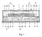
- FIG. 1 shows a section through an arrangement according to the invention of a power semiconductor module with a cooling component.
- Fig. 2 shows a three-dimensional view of a section through a second unit of an arrangement according to the invention.
- Fig. 1 shows a section through an arrangement of a power semiconductor module (1).
- This has a housing (3) with a frame-like housing part which is fixedly connected to the cooling member (2) of the arrangement.
- the frame-like housing part encloses the at least one substrate (5).
- This in turn has an insulating body (52), preferably an insulating ceramic, such as aluminum oxide or aluminum nitrite.
- the substrate (5) On the, the interior of the power semiconductor module (1) facing, the first main surface, the substrate (5) has a structured in itself Metallkaschtechnik.
- the individual sections of this metal lamination which is preferably configured as a copper lamination, form the printed conductors (54) of the power semiconductor module (1).
- the second main surface of the substrate (5) has a non-structured copper cladding (58) according to the prior art.
- controllable and / or uncontrolled power semiconductor devices such as IGBTs (insulated gate bipolar transistor) arranged in each case with antiparallel freewheeling diodes, or MOS-FETs. These are circuitally connected to other interconnects (54), for example by means of wire bonds (62) connected.
- the load connection elements (40, 42, 44) with the various necessary potentials serve for the external connection of the power electronic circuit inside the power semiconductor module (1).
- the load connection elements (40, 42, 44) are formed as metal moldings, each having a band-like portion (402, 422, 442) parallel to the substrate surface.
- the strip-like sections (402, 422, 442) in this case form a stack, wherein the band-like sections of the individual load connection elements (40, 42, 44) are spaced apart from one another exclusively by a necessary insulation, by way of example in the form of a plastic film (46). Necessary auxiliary connection elements are not shown for reasons of clarity in this sectional drawing.
- the power semiconductor module (1) preferably has an intermediate layer formed as an insulating molded body (30) between the stack of band-like sections (402, 422, 442) of the load connection elements (40, 42, 44) and the substrate (5).
- This Isolierstoffform Sciences (30) is arranged in this embodiment in the frame-like housing (3) by means of a snap-locking connection (90).
- the Isolierstoffformmaschine (30) in turn has recesses (32) for carrying out the contact feet (400, 420, 440) of the load connection elements (40, 42, 44). It is particularly preferred if these recesses (32) are designed as guides for these contact feet (400, 420, 440), whereby the positioning of the load connection elements (40, 42, 44) relative to the substrate (5) or its conductor tracks (54 ) is again improved over an arrangement with simple recesses. According to the invention, these recesses (32) have a width in any lateral direction, which is suitable for guiding the contact feet (400, 420, 440). on the other hand ensure their lateral movement up to at least 0.2mm, preferably up to 0.3mm.
- the pressure device (70) for the thermal connection of the power semiconductor module (1) with a cooling component (2) and at the same time for electrically contacting the load connection elements (40, 42, 44) with the conductor tracks (54) of the substrate (5) is formed by a pressure element ( 72) for pressure build-up and, an elastic cushion element as a pressure accumulator (74).
- the pressure is introduced via the cushion member (74) onto the stack of belt-like portions (402, 422, 442) of the load connection members (40, 42, 44) and thus exerts pressure on the contact pads (400, 420, 440). As a result, they are electrically connected to conductor tracks (54) of the substrate (5).
- Such pressure contacts (70) have proven over the life of power semiconductor modules (1) as particularly reliable contact. Also advantageous for the pressure contact is the formation of the recesses (32) of the Isolierstoffform stressess (32) as guides or shafts (34), as a result, the positioning of the contact feet (400, 420, 440) is particularly accurate.
- the pressure element (72) can be designed as a plastic molded body with a suitable inner metal core, which is designed as an example as a bimetal, and outer stiffening structures (76). It is further preferred if the pressure element (72) simultaneously serves as a cover of the power semiconductor module (1).
- the first unit of the arrangement is formed here by the cooling component (2), the housing (3) and the pressure element (72). The parts of this unit are firmly connected.
- the second unit is formed here from the substrate (5) with the circuit-connected power semiconductor components (60) and the load connection elements (40, 42, 44). The two units have no mechanically rigid connection to each other, but the second unit can move in each lateral direction at least 0.2mm, preferably 0.3mm, within the first unit.
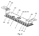
- FIG. 2 shows a three-dimensional representation of a step through a second unit of an arrangement according to the invention.
- the latter has two substrates (5) with power semiconductor components (60, 64) arranged thereon and connected in a circuit-compatible manner by means of non-illustrated bond connections.
- the circuit shown is a half-bridge circuit having a plurality of parallel-connected bipolar transistors (60, 64) forming the respective first and second switches.
- the circuit also has the necessary freewheeling diodes (64).
- the first and second switches of the half-bridge circuit are in each case distributed in half to two identical substrates (5).
- the load connection elements (40, 42, 44) of this second unit of an arrangement according to the invention and their position relative to the substrates (5) are also shown. For reasons of clarity, the insulating plastic films between the individual load connection elements (40, 42, 44) are not shown.
- the load connection elements (40, 42, 44) have a plurality of contact feet (400, 420, 440) which extend from the associated band-like sections (402, 422, 442) of the respective load connection element (40, 42, 44).
- a plurality of contact feet (400, 420, 440) of the same polarity in this case contact the associated conductor tracks (54) of the respective polarity.
- the permanently contact-safe electrical connection is formed by means of the printing device (70) described above and not shown here.
- auxiliary connection elements Shown further are recess (406, 426, 446) of the stack of load connection elements (40, 42, 44), which are provided for the arrangement of the auxiliary connection elements. It is particularly preferred if all auxiliary connection elements are arranged centrally in the longitudinal direction of the power semiconductor module (1). Accordingly, it is advantageous if all auxiliary connection elements are arranged on a longitudinal section of the power semiconductor module which has at most half the length of the power semiconductor module (1). Furthermore, it is particularly preferred if the auxiliary connection elements are designed as coil springs.
- a mechanically flexible section (408) in the course of a load connection element, in this case the AC connection (40) of the power semiconductor module (1).
- This flexible portion (408) is disposed between the band-like portion (402) above the substrates (5) and an associated contactor (404) for external electrical connection of the assembly.
- this mechanically flexible portion (408) is here designed as copper mesh, as is known for flexible load current connections outside of a power semiconductor module.
- This copper mesh is weldably joined to the contactor (404) and a continuation of the ribbon-like portion (402).
- the lateral freedom of movement of the second unit of at least two tenths of a millimeter in the housing is achieved by means of suitable guided contact devices (424, 444) of the load connection elements shown here of the DC connections (42, 44).
Landscapes
- Engineering & Computer Science (AREA)
- Microelectronics & Electronic Packaging (AREA)
- Physics & Mathematics (AREA)
- Thermal Sciences (AREA)
- Cooling Or The Like Of Semiconductors Or Solid State Devices (AREA)
Applications Claiming Priority (1)
| Application Number | Priority Date | Filing Date | Title |
|---|---|---|---|
| DE102006006424A DE102006006424B4 (de) | 2006-02-13 | 2006-02-13 | Anordnung mit mindestens einem Leistungshalbleitermodul und einem Kühlbauteil und zugehöriges Herstellungsverfahren |
Publications (3)
| Publication Number | Publication Date |
|---|---|
| EP1818982A2 true EP1818982A2 (fr) | 2007-08-15 |
| EP1818982A3 EP1818982A3 (fr) | 2010-11-10 |
| EP1818982B1 EP1818982B1 (fr) | 2014-01-01 |
Family
ID=37966749
Family Applications (1)
| Application Number | Title | Priority Date | Filing Date |
|---|---|---|---|
| EP07002032.6A Not-in-force EP1818982B1 (fr) | 2006-02-13 | 2007-01-31 | Assemblage avec au moins un module semi-conducteur de puissance et un élément de refroidissement et méthode de fabrication associée |
Country Status (4)
| Country | Link |
|---|---|
| US (1) | US7592698B2 (fr) |
| EP (1) | EP1818982B1 (fr) |
| JP (1) | JP5114065B2 (fr) |
| DE (1) | DE102006006424B4 (fr) |
Cited By (5)
| Publication number | Priority date | Publication date | Assignee | Title |
|---|---|---|---|---|
| DE102007003587A1 (de) * | 2007-01-24 | 2008-08-07 | Semikron Elektronik Gmbh & Co. Kg | Leistungshalbleitermodul mit Druckkörper |
| EP2211384A3 (fr) * | 2009-01-23 | 2010-11-03 | SEMIKRON Elektronik GmbH & Co. KG | Module semiconducteur de puissance en contact à pression avec un appareillage de refroidissement actif |
| EP2330623A1 (fr) * | 2009-12-05 | 2011-06-08 | SEMIKRON Elektronik GmbH & Co. KG | Module semi-conducteur de puissance à contact de pression doté d'éléments de raccordement de charge partiellement de type bande |
| CN103367279B (zh) * | 2012-03-30 | 2017-05-03 | 南京皓赛米电力科技有限公司 | 双面微通道液冷功率半导体整晶圆平板压接封装结构 |
| CN107026136A (zh) * | 2016-02-01 | 2017-08-08 | 赛米控电子股份有限公司 | 具有压力施加体的功率半导体模块及其布置 |
Families Citing this family (16)
| Publication number | Priority date | Publication date | Assignee | Title |
|---|---|---|---|---|
| DE102006006423B4 (de) * | 2006-02-13 | 2009-06-10 | Semikron Elektronik Gmbh & Co. Kg | Leistungshalbleitermodul und zugehöriges Herstellungsverfahren |
| DE102006006425B4 (de) * | 2006-02-13 | 2009-06-10 | Semikron Elektronik Gmbh & Co. Kg | Leistungshalbleitermodul in Druckkontaktausführung |
| DE102006052620B4 (de) * | 2006-11-08 | 2009-07-09 | Semikron Elektronik Gmbh & Co. Kg | Schaltungsanordnung mit einem Leistungsmodul, das mit einer Leiterplatte kombiniert ist. |
| DE102007045261A1 (de) * | 2007-09-21 | 2009-04-23 | Continental Automotive Gmbh | Elektrisches Gerät, insbesondere Steuergerät für ein Kraftfahrzeug |
| DE102007054709B4 (de) * | 2007-11-16 | 2014-11-13 | Semikron Elektronik Gmbh & Co. Kg | Leistungshalbleitermodul mit einem Substrat und mit einer Druckeinrichtung |
| DE102008034068B4 (de) | 2008-07-22 | 2019-07-18 | Semikron Elektronik Gmbh & Co. Kg | Leistungshalbleitermodul |
| KR101073286B1 (ko) * | 2008-12-03 | 2011-10-12 | 엘에스산전 주식회사 | 전력용 반도체 모듈 |
| DE102009046403B4 (de) * | 2009-11-04 | 2015-05-28 | Semikron Elektronik Gmbh & Co. Kg | Leistungshalbleitermodul in Druckkontakttechnik |
| DE102009057146B4 (de) * | 2009-12-05 | 2013-09-26 | Semikron Elektronik Gmbh & Co. Kg | Druckkontaktiertes Leistungshalbleitermodul mit Hybriddruckspeicher |
| DE102013200526B4 (de) | 2013-01-16 | 2019-11-21 | Semikron Elektronik Gmbh & Co. Kg | Leistungshalbleitermodul und Verfahren zur Herstellung eines Leistungshalbleitermoduls |
| DE102013104950B3 (de) * | 2013-05-14 | 2014-04-30 | Semikron Elektronik Gmbh & Co. Kg | Leistungshalbleitermodul und Anordnung hiermit |
| US9431311B1 (en) | 2015-02-19 | 2016-08-30 | Semiconductor Components Industries, Llc | Semiconductor package with elastic coupler and related methods |
| DE102015109710B4 (de) * | 2015-06-17 | 2019-10-31 | Avl Software And Functions Gmbh | Design einer Leistungszelle |
| DE102016113152B4 (de) * | 2016-07-18 | 2019-12-19 | Semikron Elektronik Gmbh & Co. Kg | Leistungselektronische Schalteinrichtung und Leistungshalbleitermodul hiermit |
| DE102017129707B4 (de) * | 2017-12-13 | 2024-12-12 | Semikron Elektronik Gmbh & Co. Kg | Verfahren zur Herstellung eines leistungselektronischen Systems |
| DE102018129336B4 (de) | 2018-11-21 | 2021-07-08 | Semikron Elektronik Gmbh & Co. Kg | Leistungshalbleitermodul mit einem Substrat und mit einem Lastanschlusselement |
Family Cites Families (16)
| Publication number | Priority date | Publication date | Assignee | Title |
|---|---|---|---|---|
| DE2942409A1 (de) * | 1979-10-19 | 1981-04-23 | Siemens AG, 1000 Berlin und 8000 München | Halbleiterbauelement mit mehreren halbleiterkoerpern |
| DE3643288A1 (de) * | 1986-12-18 | 1988-06-30 | Semikron Elektronik Gmbh | Halbleiterbaueinheit |
| US5345107A (en) * | 1989-09-25 | 1994-09-06 | Hitachi, Ltd. | Cooling apparatus for electronic device |
| DE4237632A1 (de) * | 1992-11-07 | 1994-05-11 | Export Contor Ausenhandelsgese | Schaltungsanordnung |
| JP3396566B2 (ja) * | 1995-10-25 | 2003-04-14 | 三菱電機株式会社 | 半導体装置 |
| DE19617055C1 (de) * | 1996-04-29 | 1997-06-26 | Semikron Elektronik Gmbh | Halbleiterleistungsmodul hoher Packungsdichte in Mehrschichtbauweise |
| DE19719703C5 (de) * | 1997-05-09 | 2005-11-17 | eupec Europäische Gesellschaft für Leistungshalbleiter mbH & Co. KG | Leistungshalbleitermodul mit Keramiksubstrat |
| JPH113995A (ja) * | 1997-06-12 | 1999-01-06 | Toshiba Corp | 半導体装置 |
| JPH11330283A (ja) * | 1998-05-15 | 1999-11-30 | Toshiba Corp | 半導体モジュール及び大型半導体モジュール |
| DE19903875C2 (de) * | 1999-02-01 | 2001-11-29 | Semikron Elektronik Gmbh | Leistungshalbleiterschaltungsanordnung, insbesondere Stromumrichter, in Druckkontaktierung |
| US6703707B1 (en) * | 1999-11-24 | 2004-03-09 | Denso Corporation | Semiconductor device having radiation structure |
| DE10121970B4 (de) * | 2001-05-05 | 2004-05-27 | Semikron Elektronik Gmbh | Leistungshalbleitermodul in Druckkontaktierung |
| DE10127947C1 (de) * | 2001-08-22 | 2002-10-17 | Semikron Elektronik Gmbh | Schaltungsanordnung |
| DE102004021927B4 (de) * | 2004-05-04 | 2008-07-03 | Semikron Elektronik Gmbh & Co. Kg | Verfahren zur inneren elektrischen Isolation eines Substrats für ein Leistungshalbleitermodul |
| DE102006006425B4 (de) * | 2006-02-13 | 2009-06-10 | Semikron Elektronik Gmbh & Co. Kg | Leistungshalbleitermodul in Druckkontaktausführung |
| DE102006006423B4 (de) * | 2006-02-13 | 2009-06-10 | Semikron Elektronik Gmbh & Co. Kg | Leistungshalbleitermodul und zugehöriges Herstellungsverfahren |
-
2006
- 2006-02-13 DE DE102006006424A patent/DE102006006424B4/de not_active Expired - Fee Related
-
2007
- 2007-01-31 EP EP07002032.6A patent/EP1818982B1/fr not_active Not-in-force
- 2007-02-09 JP JP2007030496A patent/JP5114065B2/ja not_active Expired - Fee Related
- 2007-02-13 US US11/705,729 patent/US7592698B2/en not_active Expired - Fee Related
Cited By (7)
| Publication number | Priority date | Publication date | Assignee | Title |
|---|---|---|---|---|
| DE102007003587A1 (de) * | 2007-01-24 | 2008-08-07 | Semikron Elektronik Gmbh & Co. Kg | Leistungshalbleitermodul mit Druckkörper |
| DE102007003587B4 (de) * | 2007-01-24 | 2009-06-10 | Semikron Elektronik Gmbh & Co. Kg | Leistungshalbleitermodul mit Druckkörper |
| EP2211384A3 (fr) * | 2009-01-23 | 2010-11-03 | SEMIKRON Elektronik GmbH & Co. KG | Module semiconducteur de puissance en contact à pression avec un appareillage de refroidissement actif |
| EP2330623A1 (fr) * | 2009-12-05 | 2011-06-08 | SEMIKRON Elektronik GmbH & Co. KG | Module semi-conducteur de puissance à contact de pression doté d'éléments de raccordement de charge partiellement de type bande |
| CN103367279B (zh) * | 2012-03-30 | 2017-05-03 | 南京皓赛米电力科技有限公司 | 双面微通道液冷功率半导体整晶圆平板压接封装结构 |
| CN107026136A (zh) * | 2016-02-01 | 2017-08-08 | 赛米控电子股份有限公司 | 具有压力施加体的功率半导体模块及其布置 |
| CN107026136B (zh) * | 2016-02-01 | 2022-02-22 | 赛米控电子股份有限公司 | 具有压力施加体的功率半导体模块及其布置 |
Also Published As
| Publication number | Publication date |
|---|---|
| US7592698B2 (en) | 2009-09-22 |
| US20070194443A1 (en) | 2007-08-23 |
| JP2007221128A (ja) | 2007-08-30 |
| JP5114065B2 (ja) | 2013-01-09 |
| DE102006006424A1 (de) | 2007-08-23 |
| DE102006006424B4 (de) | 2011-11-17 |
| EP1818982A3 (fr) | 2010-11-10 |
| EP1818982B1 (fr) | 2014-01-01 |
Similar Documents
| Publication | Publication Date | Title |
|---|---|---|
| EP1818982B1 (fr) | Assemblage avec au moins un module semi-conducteur de puissance et un élément de refroidissement et méthode de fabrication associée | |
| EP1843393B1 (fr) | Module de puissance semi-conducteur de type à contact par pression | |
| EP1830404B1 (fr) | Module semi-conducteur de puissance | |
| EP1868243B1 (fr) | Module semi-conducteur de puissance doté d'éléments de connexion isolés électriquement les uns des autres | |
| DE102017109706B3 (de) | Leistungselektronische Anordnung mit Gleichspannungsverbindungselement | |
| DE102009037257B4 (de) | Leistungshalbleitermodul mit Schaltungsträger und Lastanschlusselement sowie Herstellungsverfahren hierzu | |
| DE102015214457A1 (de) | Ansteuereinheit mit anschlüssen in federndem kontakt miteinander | |
| DE102017115883A1 (de) | Leistungselektronisches Submodul mit Gleich- und Wechselspannungsanschlusselementen und Anordnung hiermit | |
| EP4099555B1 (fr) | Demi-pont pour un entraînement électrique d'un véhicule électrique ou d'un véhicule hybride, module de puissance pour un onduleur et onduleur | |
| DE10340297B4 (de) | Verbindugsanordnung zur Verbindung von aktiven und passiven elektrischen und elektronischen Bauelementen | |
| EP2548423A1 (fr) | Circuit imprimé et appareil de commande correspondant pour véhicule à moteur | |
| DE102005055713B4 (de) | Leistungshalbleitermodul mit Anschlusselementen | |
| EP1950807B1 (fr) | Module semi-conducteur de puissance doté d'un corps de pression | |
| EP2548424B1 (fr) | Ensemble circuit et appareil de commande associé pour un véhicule automobile | |
| EP2003693B1 (fr) | Module de convertisseur de puissance triphasé contacté par pression | |
| DE102006032436A1 (de) | Vorrichtung zur Anordnung an einer Leiterplatte | |
| DE102021203704A1 (de) | Halbbrücke, Leistungsmodul und Inverter für einen elektrischen Antrieb eines Elektrofahrzeugs oder eines Hybridfahrzeugs | |
| DE102013215648A1 (de) | Leistungselektronikmodul mit Substrat, Bauelement und Leiterplatte | |
| DE102008014113B4 (de) | Leistungshalbleitermodul in Druckkontaktausführung | |
| DE102021113502A1 (de) | Elektronische Baugruppe mit Platinenverbinder, Elektronikmodul sowie Kraftfahrzeug | |
| EP2110853A2 (fr) | Agencement dans une conception de contact sous pression avec un module semi-conducteur de puissance | |
| WO2015086814A1 (fr) | Procédé de production d'un bloc et bloc |
Legal Events
| Date | Code | Title | Description |
|---|---|---|---|
| PUAI | Public reference made under article 153(3) epc to a published international application that has entered the european phase |
Free format text: ORIGINAL CODE: 0009012 |
|
| AK | Designated contracting states |
Kind code of ref document: A2 Designated state(s): AT BE BG CH CY CZ DE DK EE ES FI FR GB GR HU IE IS IT LI LT LU LV MC NL PL PT RO SE SI SK TR |
|
| AX | Request for extension of the european patent |
Extension state: AL BA HR MK YU |
|
| PUAL | Search report despatched |
Free format text: ORIGINAL CODE: 0009013 |
|
| AK | Designated contracting states |
Kind code of ref document: A3 Designated state(s): AT BE BG CH CY CZ DE DK EE ES FI FR GB GR HU IE IS IT LI LT LU LV MC NL PL PT RO SE SI SK TR |
|
| AX | Request for extension of the european patent |
Extension state: AL BA HR MK RS |
|
| 17P | Request for examination filed |
Effective date: 20101021 |
|
| RIC1 | Information provided on ipc code assigned before grant |
Ipc: H01L 23/48 20060101AFI20101116BHEP |
|
| AKX | Designation fees paid |
Designated state(s): AT BE BG CH CY CZ DE DK EE ES FI FR GB GR HU IE IS IT LI LT LU LV MC NL PL PT RO SE SI SK TR |
|
| GRAJ | Information related to disapproval of communication of intention to grant by the applicant or resumption of examination proceedings by the epo deleted |
Free format text: ORIGINAL CODE: EPIDOSDIGR1 |
|
| GRAP | Despatch of communication of intention to grant a patent |
Free format text: ORIGINAL CODE: EPIDOSNIGR1 |
|
| GRAP | Despatch of communication of intention to grant a patent |
Free format text: ORIGINAL CODE: EPIDOSNIGR1 |
|
| INTG | Intention to grant announced |
Effective date: 20130606 |
|
| INTG | Intention to grant announced |
Effective date: 20130613 |
|
| GRAS | Grant fee paid |
Free format text: ORIGINAL CODE: EPIDOSNIGR3 |
|
| GRAA | (expected) grant |
Free format text: ORIGINAL CODE: 0009210 |
|
| AK | Designated contracting states |
Kind code of ref document: B1 Designated state(s): AT BE BG CH CY CZ DE DK EE ES FI FR GB GR HU IE IS IT LI LT LU LV MC NL PL PT RO SE SI SK TR |
|
| REG | Reference to a national code |
Ref country code: GB Ref legal event code: FG4D Free format text: NOT ENGLISH |
|
| REG | Reference to a national code |
Ref country code: CH Ref legal event code: EP |
|
| REG | Reference to a national code |
Ref country code: IE Ref legal event code: FG4D Free format text: LANGUAGE OF EP DOCUMENT: GERMAN |
|
| REG | Reference to a national code |
Ref country code: DE Ref legal event code: R096 Ref document number: 502007012650 Country of ref document: DE Effective date: 20140213 |
|
| REG | Reference to a national code |
Ref country code: AT Ref legal event code: REF Ref document number: 647920 Country of ref document: AT Kind code of ref document: T Effective date: 20140215 |
|
| REG | Reference to a national code |
Ref country code: NL Ref legal event code: VDEP Effective date: 20140101 |
|
| REG | Reference to a national code |
Ref country code: LT Ref legal event code: MG4D |
|
| BERE | Be: lapsed |
Owner name: SEMIKRON ELEKTRONIK G.M.B.H. & CO. KG Effective date: 20140131 |
|
| PG25 | Lapsed in a contracting state [announced via postgrant information from national office to epo] |
Ref country code: LT Free format text: LAPSE BECAUSE OF FAILURE TO SUBMIT A TRANSLATION OF THE DESCRIPTION OR TO PAY THE FEE WITHIN THE PRESCRIBED TIME-LIMIT Effective date: 20140101 Ref country code: IS Free format text: LAPSE BECAUSE OF FAILURE TO SUBMIT A TRANSLATION OF THE DESCRIPTION OR TO PAY THE FEE WITHIN THE PRESCRIBED TIME-LIMIT Effective date: 20140501 |
|
| PG25 | Lapsed in a contracting state [announced via postgrant information from national office to epo] |
Ref country code: FI Free format text: LAPSE BECAUSE OF FAILURE TO SUBMIT A TRANSLATION OF THE DESCRIPTION OR TO PAY THE FEE WITHIN THE PRESCRIBED TIME-LIMIT Effective date: 20140101 Ref country code: CY Free format text: LAPSE BECAUSE OF FAILURE TO SUBMIT A TRANSLATION OF THE DESCRIPTION OR TO PAY THE FEE WITHIN THE PRESCRIBED TIME-LIMIT Effective date: 20140101 Ref country code: PT Free format text: LAPSE BECAUSE OF FAILURE TO SUBMIT A TRANSLATION OF THE DESCRIPTION OR TO PAY THE FEE WITHIN THE PRESCRIBED TIME-LIMIT Effective date: 20140502 Ref country code: NL Free format text: LAPSE BECAUSE OF FAILURE TO SUBMIT A TRANSLATION OF THE DESCRIPTION OR TO PAY THE FEE WITHIN THE PRESCRIBED TIME-LIMIT Effective date: 20140101 Ref country code: ES Free format text: LAPSE BECAUSE OF FAILURE TO SUBMIT A TRANSLATION OF THE DESCRIPTION OR TO PAY THE FEE WITHIN THE PRESCRIBED TIME-LIMIT Effective date: 20140101 Ref country code: SE Free format text: LAPSE BECAUSE OF FAILURE TO SUBMIT A TRANSLATION OF THE DESCRIPTION OR TO PAY THE FEE WITHIN THE PRESCRIBED TIME-LIMIT Effective date: 20140101 |
|
| REG | Reference to a national code |
Ref country code: CH Ref legal event code: PL |
|
| PG25 | Lapsed in a contracting state [announced via postgrant information from national office to epo] |
Ref country code: LV Free format text: LAPSE BECAUSE OF FAILURE TO SUBMIT A TRANSLATION OF THE DESCRIPTION OR TO PAY THE FEE WITHIN THE PRESCRIBED TIME-LIMIT Effective date: 20140101 |
|
| REG | Reference to a national code |
Ref country code: DE Ref legal event code: R097 Ref document number: 502007012650 Country of ref document: DE |
|
| PG25 | Lapsed in a contracting state [announced via postgrant information from national office to epo] |
Ref country code: MC Free format text: LAPSE BECAUSE OF FAILURE TO SUBMIT A TRANSLATION OF THE DESCRIPTION OR TO PAY THE FEE WITHIN THE PRESCRIBED TIME-LIMIT Effective date: 20140101 Ref country code: CZ Free format text: LAPSE BECAUSE OF FAILURE TO SUBMIT A TRANSLATION OF THE DESCRIPTION OR TO PAY THE FEE WITHIN THE PRESCRIBED TIME-LIMIT Effective date: 20140101 Ref country code: DK Free format text: LAPSE BECAUSE OF FAILURE TO SUBMIT A TRANSLATION OF THE DESCRIPTION OR TO PAY THE FEE WITHIN THE PRESCRIBED TIME-LIMIT Effective date: 20140101 Ref country code: EE Free format text: LAPSE BECAUSE OF FAILURE TO SUBMIT A TRANSLATION OF THE DESCRIPTION OR TO PAY THE FEE WITHIN THE PRESCRIBED TIME-LIMIT Effective date: 20140101 Ref country code: CH Free format text: LAPSE BECAUSE OF NON-PAYMENT OF DUE FEES Effective date: 20140131 Ref country code: RO Free format text: LAPSE BECAUSE OF FAILURE TO SUBMIT A TRANSLATION OF THE DESCRIPTION OR TO PAY THE FEE WITHIN THE PRESCRIBED TIME-LIMIT Effective date: 20140101 Ref country code: LI Free format text: LAPSE BECAUSE OF NON-PAYMENT OF DUE FEES Effective date: 20140131 |
|
| REG | Reference to a national code |
Ref country code: IE Ref legal event code: MM4A |
|
| PLBE | No opposition filed within time limit |
Free format text: ORIGINAL CODE: 0009261 |
|
| STAA | Information on the status of an ep patent application or granted ep patent |
Free format text: STATUS: NO OPPOSITION FILED WITHIN TIME LIMIT |
|
| PG25 | Lapsed in a contracting state [announced via postgrant information from national office to epo] |
Ref country code: SK Free format text: LAPSE BECAUSE OF FAILURE TO SUBMIT A TRANSLATION OF THE DESCRIPTION OR TO PAY THE FEE WITHIN THE PRESCRIBED TIME-LIMIT Effective date: 20140101 Ref country code: PL Free format text: LAPSE BECAUSE OF FAILURE TO SUBMIT A TRANSLATION OF THE DESCRIPTION OR TO PAY THE FEE WITHIN THE PRESCRIBED TIME-LIMIT Effective date: 20140101 |
|
| 26N | No opposition filed |
Effective date: 20141002 |
|
| REG | Reference to a national code |
Ref country code: DE Ref legal event code: R097 Ref document number: 502007012650 Country of ref document: DE Effective date: 20141002 |
|
| PG25 | Lapsed in a contracting state [announced via postgrant information from national office to epo] |
Ref country code: BE Free format text: LAPSE BECAUSE OF NON-PAYMENT OF DUE FEES Effective date: 20140131 Ref country code: IE Free format text: LAPSE BECAUSE OF NON-PAYMENT OF DUE FEES Effective date: 20140131 |
|
| REG | Reference to a national code |
Ref country code: AT Ref legal event code: MM01 Ref document number: 647920 Country of ref document: AT Kind code of ref document: T Effective date: 20140131 |
|
| PG25 | Lapsed in a contracting state [announced via postgrant information from national office to epo] |
Ref country code: SI Free format text: LAPSE BECAUSE OF FAILURE TO SUBMIT A TRANSLATION OF THE DESCRIPTION OR TO PAY THE FEE WITHIN THE PRESCRIBED TIME-LIMIT Effective date: 20140101 Ref country code: AT Free format text: LAPSE BECAUSE OF NON-PAYMENT OF DUE FEES Effective date: 20140131 |
|
| REG | Reference to a national code |
Ref country code: FR Ref legal event code: PLFP Year of fee payment: 10 |
|
| PG25 | Lapsed in a contracting state [announced via postgrant information from national office to epo] |
Ref country code: BG Free format text: LAPSE BECAUSE OF FAILURE TO SUBMIT A TRANSLATION OF THE DESCRIPTION OR TO PAY THE FEE WITHIN THE PRESCRIBED TIME-LIMIT Effective date: 20140101 |
|
| PG25 | Lapsed in a contracting state [announced via postgrant information from national office to epo] |
Ref country code: IT Free format text: LAPSE BECAUSE OF FAILURE TO SUBMIT A TRANSLATION OF THE DESCRIPTION OR TO PAY THE FEE WITHIN THE PRESCRIBED TIME-LIMIT Effective date: 20140101 Ref country code: GR Free format text: LAPSE BECAUSE OF FAILURE TO SUBMIT A TRANSLATION OF THE DESCRIPTION OR TO PAY THE FEE WITHIN THE PRESCRIBED TIME-LIMIT Effective date: 20140402 |
|
| PG25 | Lapsed in a contracting state [announced via postgrant information from national office to epo] |
Ref country code: HU Free format text: LAPSE BECAUSE OF FAILURE TO SUBMIT A TRANSLATION OF THE DESCRIPTION OR TO PAY THE FEE WITHIN THE PRESCRIBED TIME-LIMIT; INVALID AB INITIO Effective date: 20070131 Ref country code: TR Free format text: LAPSE BECAUSE OF FAILURE TO SUBMIT A TRANSLATION OF THE DESCRIPTION OR TO PAY THE FEE WITHIN THE PRESCRIBED TIME-LIMIT Effective date: 20140101 Ref country code: LU Free format text: LAPSE BECAUSE OF NON-PAYMENT OF DUE FEES Effective date: 20140131 |
|
| REG | Reference to a national code |
Ref country code: FR Ref legal event code: PLFP Year of fee payment: 11 |
|
| REG | Reference to a national code |
Ref country code: FR Ref legal event code: PLFP Year of fee payment: 12 |
|
| PGFP | Annual fee paid to national office [announced via postgrant information from national office to epo] |
Ref country code: GB Payment date: 20190206 Year of fee payment: 13 Ref country code: GB Payment date: 20190124 Year of fee payment: 13 |
|
| GBPC | Gb: european patent ceased through non-payment of renewal fee |
Effective date: 20200131 |
|
| PG25 | Lapsed in a contracting state [announced via postgrant information from national office to epo] |
Ref country code: FR Free format text: LAPSE BECAUSE OF NON-PAYMENT OF DUE FEES Effective date: 20200131 Ref country code: GB Free format text: LAPSE BECAUSE OF NON-PAYMENT OF DUE FEES Effective date: 20200131 |
|
| PGFP | Annual fee paid to national office [announced via postgrant information from national office to epo] |
Ref country code: DE Payment date: 20240131 Year of fee payment: 18 |
|
| REG | Reference to a national code |
Ref country code: DE Ref legal event code: R119 Ref document number: 502007012650 Country of ref document: DE |
|
| PG25 | Lapsed in a contracting state [announced via postgrant information from national office to epo] |
Ref country code: DE Free format text: LAPSE BECAUSE OF NON-PAYMENT OF DUE FEES Effective date: 20250801 |