EP1818983A2 - Étage de puissance d'inverseur à trois phases et assemblage - Google Patents
Étage de puissance d'inverseur à trois phases et assemblage Download PDFInfo
- Publication number
- EP1818983A2 EP1818983A2 EP07000897A EP07000897A EP1818983A2 EP 1818983 A2 EP1818983 A2 EP 1818983A2 EP 07000897 A EP07000897 A EP 07000897A EP 07000897 A EP07000897 A EP 07000897A EP 1818983 A2 EP1818983 A2 EP 1818983A2
- Authority
- EP
- European Patent Office
- Prior art keywords
- leadframes
- die
- terminals
- heat sink
- power
- Prior art date
- Legal status (The legal status is an assumption and is not a legal conclusion. Google has not performed a legal analysis and makes no representation as to the accuracy of the status listed.)
- Withdrawn
Links
Images






Classifications
-
- H—ELECTRICITY
- H10—SEMICONDUCTOR DEVICES; ELECTRIC SOLID-STATE DEVICES NOT OTHERWISE PROVIDED FOR
- H10W—GENERIC PACKAGES, INTERCONNECTIONS, CONNECTORS OR OTHER CONSTRUCTIONAL DETAILS OF DEVICES COVERED BY CLASS H10
- H10W90/00—Package configurations
-
- H—ELECTRICITY
- H02—GENERATION; CONVERSION OR DISTRIBUTION OF ELECTRIC POWER
- H02M—APPARATUS FOR CONVERSION BETWEEN AC AND AC, BETWEEN AC AND DC, OR BETWEEN DC AND DC, AND FOR USE WITH MAINS OR SIMILAR POWER SUPPLY SYSTEMS; CONVERSION OF DC OR AC INPUT POWER INTO SURGE OUTPUT POWER; CONTROL OR REGULATION THEREOF
- H02M7/00—Conversion of AC power input into DC power output; Conversion of DC power input into AC power output
- H02M7/003—Constructional details, e.g. physical layout, assembly, wiring or busbar connections
-
- H—ELECTRICITY
- H10—SEMICONDUCTOR DEVICES; ELECTRIC SOLID-STATE DEVICES NOT OTHERWISE PROVIDED FOR
- H10W—GENERIC PACKAGES, INTERCONNECTIONS, CONNECTORS OR OTHER CONSTRUCTIONAL DETAILS OF DEVICES COVERED BY CLASS H10
- H10W44/00—Electrical arrangements for controlling or matching impedance
- H10W44/501—Inductive arrangements
-
- H—ELECTRICITY
- H10—SEMICONDUCTOR DEVICES; ELECTRIC SOLID-STATE DEVICES NOT OTHERWISE PROVIDED FOR
- H10W—GENERIC PACKAGES, INTERCONNECTIONS, CONNECTORS OR OTHER CONSTRUCTIONAL DETAILS OF DEVICES COVERED BY CLASS H10
- H10W72/00—Interconnections or connectors in packages
- H10W72/071—Connecting or disconnecting
- H10W72/075—Connecting or disconnecting of bond wires
- H10W72/07551—Connecting or disconnecting of bond wires characterised by changes in properties of the bond wires during the connecting
- H10W72/07552—Connecting or disconnecting of bond wires characterised by changes in properties of the bond wires during the connecting changes in structures or sizes
-
- H—ELECTRICITY
- H10—SEMICONDUCTOR DEVICES; ELECTRIC SOLID-STATE DEVICES NOT OTHERWISE PROVIDED FOR
- H10W—GENERIC PACKAGES, INTERCONNECTIONS, CONNECTORS OR OTHER CONSTRUCTIONAL DETAILS OF DEVICES COVERED BY CLASS H10
- H10W72/00—Interconnections or connectors in packages
- H10W72/50—Bond wires
- H10W72/521—Structures or relative sizes of bond wires
- H10W72/527—Multiple bond wires having different sizes
-
- H—ELECTRICITY
- H10—SEMICONDUCTOR DEVICES; ELECTRIC SOLID-STATE DEVICES NOT OTHERWISE PROVIDED FOR
- H10W—GENERIC PACKAGES, INTERCONNECTIONS, CONNECTORS OR OTHER CONSTRUCTIONAL DETAILS OF DEVICES COVERED BY CLASS H10
- H10W72/00—Interconnections or connectors in packages
- H10W72/50—Bond wires
- H10W72/531—Shapes of wire connectors
- H10W72/5363—Shapes of wire connectors the connected ends being wedge-shaped
-
- H—ELECTRICITY
- H10—SEMICONDUCTOR DEVICES; ELECTRIC SOLID-STATE DEVICES NOT OTHERWISE PROVIDED FOR
- H10W—GENERIC PACKAGES, INTERCONNECTIONS, CONNECTORS OR OTHER CONSTRUCTIONAL DETAILS OF DEVICES COVERED BY CLASS H10
- H10W72/00—Interconnections or connectors in packages
- H10W72/50—Bond wires
- H10W72/541—Dispositions of bond wires
- H10W72/5445—Dispositions of bond wires being orthogonal to a side surface of the chip, e.g. parallel arrangements
-
- H—ELECTRICITY
- H10—SEMICONDUCTOR DEVICES; ELECTRIC SOLID-STATE DEVICES NOT OTHERWISE PROVIDED FOR
- H10W—GENERIC PACKAGES, INTERCONNECTIONS, CONNECTORS OR OTHER CONSTRUCTIONAL DETAILS OF DEVICES COVERED BY CLASS H10
- H10W72/00—Interconnections or connectors in packages
- H10W72/50—Bond wires
- H10W72/541—Dispositions of bond wires
- H10W72/547—Dispositions of multiple bond wires
- H10W72/5475—Dispositions of multiple bond wires multiple bond wires connected to common bond pads at both ends of the wires
-
- H—ELECTRICITY
- H10—SEMICONDUCTOR DEVICES; ELECTRIC SOLID-STATE DEVICES NOT OTHERWISE PROVIDED FOR
- H10W—GENERIC PACKAGES, INTERCONNECTIONS, CONNECTORS OR OTHER CONSTRUCTIONAL DETAILS OF DEVICES COVERED BY CLASS H10
- H10W90/00—Package configurations
- H10W90/811—Multiple chips on leadframes
Definitions
- This invention relates to electrical power supplies and more specifically relates to a three phase inverter which can be employed in an automotive or other application.
- Multiphase inverter circuits and assemblies are well known and are shown for example in U.S. patents 5,966,291 ; 6,320,747 ; 6,326,761 ; 6,700,191 and 6,703,703 .
- Such devices generally employ leadframes which carry MOSFETs, IGBTs or other switching devices arranged in a three phase bridge and assembled in sealed housings which may be air or water cooled.
- Such circuits are needed for many applications, such as automotive applications for producing a three phase a-c output from the d-c automotive battery for driving three phase motors or the like.
- circuit and its housing should be low cost, low volume, and easily installed and maintained.
- a novel leadframe assembly in which a plurality of individual insulated leadframes; B(-); B(+) and three ac leadframes as for phases U, W and V are provided and located in a common plane.
- These leadframes carry a plurality of semiconductor devices using an insulated circuit board glued to selected leadframes as a mechanical interconnection element having also the function of routing electrical signals from one leadframe to the others. This is done after the semiconductor device die have been attached, as by solder, to the insulated frames. Therefore, the processes used for attaching the semiconductor device die are not limited by the glass transition temperature of the insulated circuit board.
- the invention then allows the assembly of testable sub-modules. Furthermore, this configuration allows the realization of an insulated multilayer bus-structure which provides a layout pattern which permits easy cooling.
- the leadframes are attached to a heat-sink in an insulating manner.
- the heat-sink contains a liquid cooling channel and the points of fixation or mounting for the inverter.
- a printed circuit board which is glued on top of the leadframes provides the interconnections for controlling the semiconductor devices.
- a support frame, placed on top of leadframes and glued and bolted to the heat-sink holds current sensing elements, the controller circuitry board, and fixes the leadframes together.
- An EMI shield screens the entire power stage and controller.
- a cover seals the arrangement and provides the fixation of the electrical terminals and connectors.
- Figure 1 is a circuit diagram of the inverter structure of the invention.
- Figure 2 is a top plan view of the assembled leadframes of the invention.
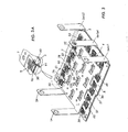
- Figure 3 is a perspective view of the assembly of Figure 2.
- Figure 3A is a detail view of the circled area in Figure 3.
- Figure 4 shows the path of the cooling channel in a heat sink beneath the leadframes of Figure 1.
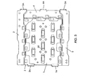
- Figure 5 is a plan view of the leadframes of Figure 1 without the die or wire bonds in place to show the substantial coplanarity of the leadframes.
- Figure 6 is an exploded perspective view of the leadframes and insulation printed circuit board (PCB) of Figures 1 and 5.
- PCB printed circuit board
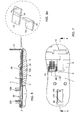
- Figure 7 is a detailed top view of a die mounted on a leadframe in Figure 1.
- Figure 8 is a cross-section of Figure 7 taken across section line 8-8 in Figure 7.
- Figure 8A is a detail showing the bending of a leadframe extension in Figure 8 to form a power terminal which extends perpendicularly from the plane of the leadframe.
- Figure 9 is a partly cut-away view of the leadframe assembly of Figures 2 to 8 assembled on a heat sink.
- Figure 9A is a detail of the capacitor connection terminals in Figure 9.
- Figure 10 is an exploded perspective view of the housing and leadframe assembly.
- Figure 11 shows the assembly of Figure 10 without the top cover.
- Figure 12 is a cross-section detail of the seal between the cover and heatsink of Figure 10.
- Figure 13 and 14 show two respective isometric views of the assembly of Figure 10.
- Figure 15 is a cross-sectional detail of the connector bolt of Figures 10, 13 and 14.
- FIG. 1 there is shown a conventional three phase inverter circuit.
- the circuit comprises d-c input terminals 1A, 1B and three phase output terminals 3A, 3B and 3C for phases U, W and V respectively.
- a filter capacitor 122 is connected across the d-c input terminals, and MOSgated semiconductor device switches inlcuding MOSgated devices 30, 40 for phase U, 33, 50 for phase W and 36, 60 for phase V are provided.
- each leg of the bridge has 3 parallel connected MOSgated devices as will be later described.
- the invention deals with the novel implementation and packaging of multiphase circuits like that of Figure 1.
- Figures 2 through 8 show a novel leadframe arrangement for carrying out the circuit of Figure 1.
- 5 leadframes insulated from one another and generally coplanar to one another are provided, including B(-) leadframe, B(+) leadframe 2 and AC phase leadframes 3, 4 and 5, corresponding to phases U, W and V respectively.
- Leadframes 1 to 5 are thin conductive members which may be suitably stamped or etched, to a given pattern using well known techniques.
- Each of leadframes have perpendicularly extending terminals 1A, 2A, 3A, 4A and 5A, respectively bent upwardly from the flat as shown in Figure 8A for B(+) lead 1A.
- Note groove 1B in Figure 8 which facilitates the bend.
- Leadframes 1 and 2 overlap one another as shown in Figure 8 and are secured to one another but insulated from one another by a suitable insulation cement 9 ( Figures 6 and 8A) or the like.
- Leadframes 3, 4 and 5 are located adjacent to but are spaced from the two sides and one edge of the combined leadframes 1 and 2 as may be best seen in Figure 5.
- circuit board 7 which carries the necessary control circuitry and conductive traces leading to the control elements (gate electrodes and current sense circuits) of the various devices mounted on the leadframes as will be described.
- Circuit board 7 is glued atop the leadframes as by the insulation cement 11 in Figures 6 and 8.
- Leadframes 1 and 2 have aligned openings, such as openings 20 which permit passage of capacitor terminals, as will be described.
- the leadframes also carry Hall-effect sensors, such as sensors 21 and 22 on leadframes 3 and 5 respectively ( Figure 2) which are used to monitor the current in phases U, V and W as will be later described.
- Each of the leadframes 2, 3, 4 and 5 have MOSgated die such as MOSFET (FEDT) die soldered thereto before the assembly of the leadframes relative to one another.
- MOSFET MOSFET
- nine MOSFETs (3 parallel FETs for each phase) 30 to 38 have their bottom drain electrodes soldered around the periphery of B(+) leadframe 2; three FETs 40, 41, 42 are soldered to leadframe 3; three FETs 50, 51, 52 are soldered to leadframe 4, and three FETs 60, 61, 62 are soldered to leadframe 5.
- Figures 3A, 7 and 8 show the typical connection of die 38 to leadframe 2, using a conventional heat spreader and solder connection 70.
- the source electrodes of all of the FET die are connected to and adjacent one of the phase leadframes 3, 4 and 5 or the B(-) leadframe 1.
- the sources of FETs 40,41,42, 50, 51, 52 and 60, 61 and 62 are wire bonded to the B(-) leadframe 1.
- the sources of FETs 30, 31, 32 are bonded to leadframe 3 of phase U.
- the sources of FETs 33, 34 and 35 are bonded to leadframe 4 (phase W).
- the sources of FETs 36, 37 and 38 are each bonded to leadframe 5 (phase V).
- PCB 7 has projection such as projection 7A, 7B, 7C at each FET location which has traces which are wire bonded to the gate electrodes of their respective die as by wire bonds 90 ( Figure 3A) and to leadframe 1 as by wire bonds 91 ( Figure 3A).
- Figures 9 to 15 show the novel housing for the leadframe assembly of Figures 2 through 8.
- the assembly of Figures 2 through 8 is shown in Figure 10 as assembly 110.
- the assembly 110 as shown in Figures 9, 10 and 11, is mounted on a heat sink 120 and is insulated there from by a thin insulation sheet 121.
- Heat sink 120 contains cavities for mounting 9 capacitors 122.
- the capacitor terminals 123, 124 ( Figure 9A) may extend through openings 20 and spot welded to up-bended projections 125, 126 respectively of the B(-) and B(+) leadframes 2 and 1.
- Heat sink 120 also includes suitable mounting flanges 130, 131 and other bolt openings to enable mounting of the fully assembled structure to a motor or generator or the like.
- Heat sink 120 further contains a water flow channel 140 which follows the path 100 ( Figure 4) under the power FETs or die of the leadframe 110.
- Channel 140 has coolant inlet and outlet fittings 141 and 142. If desired, the heat sink 120 can be air cooled.
- a contact block 150 for PCB 7 is then mounted in place and a spacer 151 is fixed over the surface of assembly 110 ( Figures 10 and 11).
- An insulation frame 160 receives terminals 1A through 5A and is suitably clamped or fixed to heat sink 120.
- Support frame 160 carries C shaped rings 170 and 171 of magnetic material, which receive terminals 1A and 1B, and C ring magnetic sensors 175, 176 which receive the Hall sensors 22 and 21 respectively of Figure 2. These sensors are employed to measure the inverter currents in the B(-) and B(+) terminals, and phases U, W and V. and can cooperate with circuitry carried on circuit board 180 ( Figure 10) and the PCB 7.
- Spacer 151 helps to prevent excessive vibration of circuit board 180.
- Connector 150 ( Figure 11), which may function as a ground connector, also supports board 180 of Figure 10.
- a signal connector structure 190 of Figure 10 is connected to circuit board 180 and is shielded against electromagnetic interference by a suitable shield 191 ( Figures 10 and 12). If desired, cover 200 can be of metal, so that EMI shield 191 can be eliminated.
- the housing is completed by an insulation cover 200.
- Cover 200 is suitably fixed to heat sink 120 and is sealed thereto as by an O-ring seal 201 ( Figure 12).
- Cover 200 also receives terminal bolts 210, 211, 212, 213 and 214 for terminals B(-), B(+), phase U, phase W and phase V respectively. These terminal bolts are sealed by O-ring seals such as seal 220 ( Figures 10 and 15).
- a vent opening 230 in Figure 10 may be provided to enable venting of the module interior and opening 230 can be sealed by cap 235 as desired.
Landscapes
- Engineering & Computer Science (AREA)
- Power Engineering (AREA)
- Inverter Devices (AREA)
- Lead Frames For Integrated Circuits (AREA)
Applications Claiming Priority (3)
| Application Number | Priority Date | Filing Date | Title |
|---|---|---|---|
| US75949906P | 2006-01-17 | 2006-01-17 | |
| US75950006P | 2006-01-17 | 2006-01-17 | |
| US11/623,520 US20070165376A1 (en) | 2006-01-17 | 2007-01-16 | Three phase inverter power stage and assembly |
Publications (2)
| Publication Number | Publication Date |
|---|---|
| EP1818983A2 true EP1818983A2 (fr) | 2007-08-15 |
| EP1818983A3 EP1818983A3 (fr) | 2009-07-29 |
Family
ID=38219146
Family Applications (1)
| Application Number | Title | Priority Date | Filing Date |
|---|---|---|---|
| EP07000897A Withdrawn EP1818983A3 (fr) | 2006-01-17 | 2007-01-17 | Étage de puissance d'inverseur à trois phases et assemblage |
Country Status (2)
| Country | Link |
|---|---|
| US (1) | US20070165376A1 (fr) |
| EP (1) | EP1818983A3 (fr) |
Cited By (5)
| Publication number | Priority date | Publication date | Assignee | Title |
|---|---|---|---|---|
| EP2432106A4 (fr) * | 2008-02-06 | 2012-12-26 | Honda Motor Co Ltd | Véhicule électrique et procédé de refroidissement de convertisseur c.c./c.c. de véhicule |
| KR20170090135A (ko) * | 2016-01-28 | 2017-08-07 | 엘지이노텍 주식회사 | 인버터 패키지 |
| EP2584690A4 (fr) * | 2010-06-21 | 2018-02-28 | Hitachi Automotive Systems, Ltd. | Dispositif de conversion de puissance |
| WO2018069174A1 (fr) * | 2016-10-11 | 2018-04-19 | HELLA GmbH & Co. KGaA | Système comportant un support et une électronique et procédé de fabrication d'un support |
| IT201700033230A1 (it) * | 2017-03-27 | 2018-09-27 | S M E S P A | Modulo di potenza per un convertitore di grandezze elettriche |
Families Citing this family (67)
| Publication number | Priority date | Publication date | Assignee | Title |
|---|---|---|---|---|
| DE10258035A1 (de) * | 2002-12-12 | 2004-06-24 | Robert Bosch Gmbh | Einphasiges Stromrichtermodul |
| US7710723B2 (en) * | 2007-07-17 | 2010-05-04 | Gm Global Technology Operations, Inc. | Vehicle inverter assembly with cooling channels |
| JP4452953B2 (ja) * | 2007-08-09 | 2010-04-21 | 日立オートモティブシステムズ株式会社 | 電力変換装置 |
| US8059404B2 (en) * | 2008-10-09 | 2011-11-15 | GM Global Technology Operations LLC | Power inverters |
| JP4775475B2 (ja) * | 2009-04-14 | 2011-09-21 | 株式会社デンソー | 電力変換装置 |
| US20110116235A1 (en) * | 2009-11-13 | 2011-05-19 | Lg Electronics Inc. | Motor drive unit and vehicle including the same |
| JP5158176B2 (ja) * | 2010-02-05 | 2013-03-06 | 株式会社デンソー | 電力変換装置 |
| JP5423654B2 (ja) * | 2010-02-05 | 2014-02-19 | 株式会社デンソー | 電力変換装置 |
| JP5327195B2 (ja) * | 2010-02-05 | 2013-10-30 | 株式会社デンソー | 電力変換装置 |
| JP5423655B2 (ja) * | 2010-02-05 | 2014-02-19 | 株式会社デンソー | 電力変換装置 |
| JP4924750B2 (ja) * | 2010-02-05 | 2012-04-25 | 株式会社デンソー | 電力変換装置 |
| US8446726B2 (en) * | 2010-10-28 | 2013-05-21 | Infineon Technologies Ag | Semiconductor module having an insert and method for producing a semiconductor module having an insert |
| EP2447990B1 (fr) * | 2010-11-02 | 2020-12-23 | ABB Power Grids Switzerland AG | Plaque de base |
| JP5455888B2 (ja) * | 2010-12-27 | 2014-03-26 | 日立オートモティブシステムズ株式会社 | 車両用電力変換装置 |
| JP5417314B2 (ja) * | 2010-12-27 | 2014-02-12 | 日立オートモティブシステムズ株式会社 | 電力変換装置 |
| JP5776390B2 (ja) * | 2011-07-13 | 2015-09-09 | 富士電機株式会社 | 鉄道車両用電力変換装置 |
| US8964401B2 (en) | 2011-10-14 | 2015-02-24 | Sunpower Corporation | Electrical insulator casing |
| JP5743851B2 (ja) * | 2011-10-31 | 2015-07-01 | 日立オートモティブシステムズ株式会社 | 電子装置 |
| AU2012232967B2 (en) * | 2011-10-31 | 2015-01-15 | Abb Technology Ag | Cabinet with modules having a thermosiphon cooler arrangement |
| AU2012232968B2 (en) | 2011-10-31 | 2014-11-13 | Abb Technology Ag | Thermosiphon cooler arrangement in modules with electric and/or electronic components |
| WO2013095490A1 (fr) * | 2011-12-22 | 2013-06-27 | Hewlett-Packard Development Company, L.P. | Base et blindage de dissipateur thermique |
| CN102646648B (zh) * | 2012-03-30 | 2014-12-03 | 台达电子企业管理(上海)有限公司 | 半导体开关绝缘保护装置以及电源组件 |
| JP5738794B2 (ja) * | 2012-03-30 | 2015-06-24 | 日立オートモティブシステムズ株式会社 | 電力変換装置 |
| US8755195B2 (en) * | 2012-06-08 | 2014-06-17 | Lsi Corporation | ESD discharge path on chasis-mounted PCB assembly |
| KR20140006392A (ko) * | 2012-07-05 | 2014-01-16 | 엘에스산전 주식회사 | 자동차용 전장부품 박스 |
| US9370994B2 (en) * | 2012-08-24 | 2016-06-21 | Nissan Motor Co., Ltd. | Integrated power electric unit mounted on electric vehicle |
| JP2014063930A (ja) * | 2012-09-21 | 2014-04-10 | Hitachi Automotive Systems Ltd | 電子制御装置 |
| TWI491347B (zh) * | 2012-10-24 | 2015-07-01 | Hon Hai Prec Ind Co Ltd | 散熱板及封裝殼體 |
| US20140140010A1 (en) * | 2012-11-16 | 2014-05-22 | Lien Chang Electronic Enterprise Co., Ltd. | Current converting device |
| JP2014138445A (ja) * | 2013-01-15 | 2014-07-28 | Toyota Motor Corp | 電力変換装置 |
| US9482700B2 (en) * | 2013-01-20 | 2016-11-01 | Lenovo Enterprise Solutions (Singapore) Pte. Ltd. | Current detector to sense current without being in series with conductor |
| CN203243595U (zh) * | 2013-03-07 | 2013-10-16 | 杭州华三通信技术有限公司 | 一种pcb结构 |
| CN103237412B (zh) * | 2013-03-27 | 2016-03-23 | 苏州远创达科技有限公司 | 一种电子件安装结构及制作方法、电子件产品 |
| KR102148201B1 (ko) * | 2013-05-06 | 2020-08-26 | 삼성전자주식회사 | 제어장치 |
| EP2874479B1 (fr) * | 2013-06-19 | 2018-08-08 | Amogreentech Co., Ltd. | Feuille isolante hybride et équipement électronique doté de cette dernière |
| JP6149611B2 (ja) * | 2013-08-29 | 2017-06-21 | アイシン・エィ・ダブリュ株式会社 | インバータ装置及び車両用駆動装置 |
| JP5880519B2 (ja) * | 2013-10-21 | 2016-03-09 | トヨタ自動車株式会社 | 車載電子装置 |
| CN104682670B (zh) * | 2013-11-26 | 2017-12-12 | 台达电子企业管理(上海)有限公司 | 电源转换装置与其电源转换板组件 |
| CN104684338B (zh) * | 2013-11-26 | 2018-01-30 | 台达电子企业管理(上海)有限公司 | 散热基座与电子装置 |
| DE102014208594A1 (de) * | 2014-05-08 | 2015-11-12 | Zf Friedrichshafen Ag | Leistungselektronikanordnung |
| US9166309B1 (en) * | 2014-06-27 | 2015-10-20 | Tyco Electronics Corporation | Bus bar with connector shroud |
| DE112015003244T5 (de) * | 2014-09-25 | 2017-04-13 | Hitachi Automotive Systems, Ltd. | Leistungsumsetzer |
| KR102286337B1 (ko) * | 2014-10-17 | 2021-08-04 | 쓰리엠 이노베이티브 프로퍼티즈 컴파니 | 전자파 차폐 구조물과 방열패드 및 이들을 포함하는 전자회로기판 조립체 |
| US9601963B2 (en) * | 2014-10-20 | 2017-03-21 | Asia Vital Components Co., Ltd. | Motor waterproof structure |
| US9420724B2 (en) * | 2014-11-04 | 2016-08-16 | Ge Aviation Systems Llc | Power converter assembly |
| US9674990B2 (en) * | 2015-01-23 | 2017-06-06 | Rockwell Automation Technoloies, Inc. | Devices and methods for cooling bus capacitors |
| US9923324B2 (en) * | 2015-01-31 | 2018-03-20 | Ixys Corporation | AC line filter and AC-to-DC rectifier module |
| FR3042078B1 (fr) * | 2015-10-05 | 2019-03-22 | Valeo Equipements Electriques Moteur | Module electronique de puissance |
| EP3206468B1 (fr) * | 2016-02-15 | 2018-12-26 | Siemens Aktiengesellschaft | Convertisseur doté d'un circuit intermédiaire à tension continue |
| KR101835954B1 (ko) * | 2016-02-24 | 2018-04-19 | 엘에스산전 주식회사 | 전동기 구동 장치 |
| JP6768340B2 (ja) * | 2016-04-28 | 2020-10-14 | 株式会社東芝 | 鉄道車両の電力変換装置 |
| US10204847B2 (en) * | 2016-10-06 | 2019-02-12 | Infineon Technologies Americas Corp. | Multi-phase common contact package |
| US12225657B2 (en) * | 2017-01-03 | 2025-02-11 | Transportation Ip Holdings, Llc | Power system and method for controlling power modules |
| JP6440779B1 (ja) * | 2017-07-04 | 2018-12-19 | 三菱電機株式会社 | 電力変換装置 |
| JP6838537B2 (ja) * | 2017-09-26 | 2021-03-03 | 株式会社デンソー | 電力変換装置 |
| DE102019205964A1 (de) * | 2018-04-25 | 2019-10-31 | Nidec Corporation | Invertersteuervorrichtung |
| JP6920247B2 (ja) * | 2018-05-21 | 2021-08-18 | 日立Astemo株式会社 | 電力変換装置 |
| US11489453B2 (en) * | 2018-05-25 | 2022-11-01 | Miba Energy Holding Gmbh | Power module with defined charge-reversal path and production method |
| JP7518601B2 (ja) * | 2018-06-05 | 2024-07-18 | 日本ケミコン株式会社 | バスバー積層体及びそれを備える電子部品実装モジュール、バスバー積層体の製造方法 |
| DE102018121945A1 (de) * | 2018-09-07 | 2020-03-12 | Seg Automotive Germany Gmbh | Leistungsmodul für einen Inverter, Inverter und Verfahren zum Herstellen eines Leistungsmoduls |
| DE102018121919A1 (de) * | 2018-09-07 | 2020-03-12 | Seg Automotive Germany Gmbh | Leistungsmodul für einen Inverter, Inverter und Verfahren zum Herstellen eines Leistungsmoduls |
| US10807730B2 (en) * | 2018-12-21 | 2020-10-20 | General Electric Company | Motor driven propulsor of an aircraft |
| DE102019220010A1 (de) * | 2019-12-18 | 2021-06-24 | Zf Friedrichshafen Ag | Halbbrückenmodul eines Traktionsinverters einer Leistungselektronik eines Elektrofahrzeugs oder Hybridfahrzeugs |
| EP3876688B1 (fr) * | 2020-03-03 | 2024-01-31 | Honeywell International Inc. | Appareil de connexion de cartes de circuits imprimés doté d'un élément électrique à température variable |
| US11670929B2 (en) * | 2021-06-02 | 2023-06-06 | Schaeffler Technologies AG & Co. KG | Heat dissipation and sealing configuration for junction assembly |
| DE102021213929A1 (de) | 2021-12-08 | 2023-06-15 | Zf Friedrichshafen Ag | Wechselrichter für einen elektrischen Antriebsstrang eines Fahrzeugs und Verfahren zum Herstellen eines Wechselrichters |
| CN217957565U (zh) * | 2022-04-28 | 2022-12-02 | 华为数字能源技术有限公司 | 封装结构 |
Family Cites Families (23)
| Publication number | Priority date | Publication date | Assignee | Title |
|---|---|---|---|---|
| JPS60239051A (ja) * | 1984-05-11 | 1985-11-27 | Mitsubishi Electric Corp | 半導体装置 |
| JPH0740790B2 (ja) * | 1987-02-23 | 1995-05-01 | 株式会社東芝 | 大電力パワ−モジユ−ル |
| US5504655A (en) * | 1994-06-10 | 1996-04-02 | Westinghouse Electric Corp. | Electric vehicle power distribution module |
| US5517063A (en) * | 1994-06-10 | 1996-05-14 | Westinghouse Electric Corp. | Three phase power bridge assembly |
| JP3299421B2 (ja) * | 1995-10-03 | 2002-07-08 | 三菱電機株式会社 | 電力用半導体装置の製造方法およびリードフレーム |
| DE19645636C1 (de) * | 1996-11-06 | 1998-03-12 | Telefunken Microelectron | Leistungsmodul zur Ansteuerung von Elektromotoren |
| DE19722355A1 (de) * | 1997-05-28 | 1998-12-03 | Bosch Gmbh Robert | Verfahren zur Herstellung elektrischer Baugruppen und elektrische Baugruppe |
| US6078501A (en) * | 1997-12-22 | 2000-06-20 | Omnirel Llc | Power semiconductor module |
| US6249024B1 (en) * | 1998-12-09 | 2001-06-19 | International Rectifier Corp. | Power module with repositioned positive and reduced inductance and capacitance |
| DE19913450A1 (de) * | 1999-03-25 | 2000-09-28 | Mannesmann Sachs Ag | Leistungselektronik zum Steuern einer elektrischen Maschine |
| DE10101086B4 (de) * | 2000-01-12 | 2007-11-08 | International Rectifier Corp., El Segundo | Leistungs-Moduleinheit |
| JP2001308566A (ja) * | 2000-04-26 | 2001-11-02 | Auto Network Gijutsu Kenkyusho:Kk | 車両用制御ユニットの冷却構造 |
| JP3642012B2 (ja) * | 2000-07-21 | 2005-04-27 | 株式会社日立製作所 | 半導体装置,電力変換装置及び自動車 |
| US7012810B2 (en) * | 2000-09-20 | 2006-03-14 | Ballard Power Systems Corporation | Leadframe-based module DC bus design to reduce module inductance |
| JP2002246515A (ja) * | 2001-02-20 | 2002-08-30 | Mitsubishi Electric Corp | 半導体装置 |
| DE10114125A1 (de) * | 2001-03-22 | 2002-09-26 | Isad Electronic Sys Gmbh & Co | Aus mehreren Leistungsmodulen bestehende elektronische Leistungsschaltung |
| JP4357762B2 (ja) * | 2001-03-30 | 2009-11-04 | 株式会社オートネットワーク技術研究所 | 車両用パワーディストリビュータ |
| JP2002359329A (ja) * | 2001-05-30 | 2002-12-13 | Hitachi Ltd | 半導体装置 |
| JP3676719B2 (ja) * | 2001-10-09 | 2005-07-27 | 株式会社日立製作所 | 水冷インバータ |
| US6982873B2 (en) * | 2002-01-16 | 2006-01-03 | Rockwell Automation Technologies, Inc. | Compact vehicle drive module having improved thermal control |
| EP1363026A3 (fr) * | 2002-04-26 | 2004-09-01 | Denso Corporation | Onduleur intégré moteur pour un véhicule automobile |
| FR2853808B1 (fr) * | 2003-04-09 | 2006-09-15 | Alstom | Module de commutation de puissance et ondulateur equipe de ce module |
| JP2005136264A (ja) * | 2003-10-31 | 2005-05-26 | Mitsubishi Electric Corp | 電力用半導体装置及び電力用半導体モジュール |
-
2007
- 2007-01-16 US US11/623,520 patent/US20070165376A1/en not_active Abandoned
- 2007-01-17 EP EP07000897A patent/EP1818983A3/fr not_active Withdrawn
Cited By (8)
| Publication number | Priority date | Publication date | Assignee | Title |
|---|---|---|---|---|
| EP2432106A4 (fr) * | 2008-02-06 | 2012-12-26 | Honda Motor Co Ltd | Véhicule électrique et procédé de refroidissement de convertisseur c.c./c.c. de véhicule |
| EP2584690A4 (fr) * | 2010-06-21 | 2018-02-28 | Hitachi Automotive Systems, Ltd. | Dispositif de conversion de puissance |
| KR20170090135A (ko) * | 2016-01-28 | 2017-08-07 | 엘지이노텍 주식회사 | 인버터 패키지 |
| WO2018069174A1 (fr) * | 2016-10-11 | 2018-04-19 | HELLA GmbH & Co. KGaA | Système comportant un support et une électronique et procédé de fabrication d'un support |
| IT201700033230A1 (it) * | 2017-03-27 | 2018-09-27 | S M E S P A | Modulo di potenza per un convertitore di grandezze elettriche |
| WO2018178855A1 (fr) * | 2017-03-27 | 2018-10-04 | S.M.E S.P.A. | Module d'alimentation en demi-pont à faible inductance |
| CN110506384A (zh) * | 2017-03-27 | 2019-11-26 | Sme股份公司 | 低电感半桥功率模块 |
| CN110506384B (zh) * | 2017-03-27 | 2022-02-11 | Sme股份公司 | 低电感半桥功率模块 |
Also Published As
| Publication number | Publication date |
|---|---|
| EP1818983A3 (fr) | 2009-07-29 |
| US20070165376A1 (en) | 2007-07-19 |
Similar Documents
| Publication | Publication Date | Title |
|---|---|---|
| EP1818983A2 (fr) | Étage de puissance d'inverseur à trois phases et assemblage | |
| JP7297815B2 (ja) | パワーデバイスを並列接続するための低インダクタンスおよび高速スイッチングを有するハイパワー多層モジュール | |
| US11445630B2 (en) | High power multilayer module having low inductance and fast switching for paralleling power devices | |
| JP7655891B2 (ja) | 低インダクタンスおよび高速スイッチングを有する、パワーデバイスを並列化するための高電力多層モジュール | |
| JP6412612B2 (ja) | ハーフブリッジを設けるパワーモジュール、ならびにパワーモジュールおよびキャパシタの配置 | |
| US5966291A (en) | Power module for the control of electric motors | |
| JP3501685B2 (ja) | 電力変換装置 | |
| US20220354014A1 (en) | High power multilayer module having low inductance and fast switching for paralleling power devices | |
| KR100305251B1 (ko) | 전력변환장치 | |
| US12087680B2 (en) | Power module having an elevated power plane with an integrated signal board and process of implementing the same | |
| CN106953504B (zh) | 电子的线路单元 | |
| CN105470248B (zh) | 半导体器件 | |
| US20070290311A1 (en) | Bond wireless power module wiht double-sided single device cooling and immersion bath cooling | |
| CN116325135B (zh) | 半导体封装、半导体装置以及电力变换装置 | |
| WO2011145219A1 (fr) | Module semi-conducteur de puissance | |
| CN105874596A (zh) | 半导体模块 | |
| EP1378941B1 (fr) | Module semi-conductrice et convertisseur à haut prestation | |
| TW201843805A (zh) | 電子裝置 | |
| WO2020229113A1 (fr) | Module semi-conducteur | |
| CN101276806A (zh) | 具有双边的单器件冷却和浸浴冷却的无线连接功率模块 | |
| WO2025237528A1 (fr) | Module semi-conducteur de puissance et procédé de fabrication de module semi-conducteur de puissance |
Legal Events
| Date | Code | Title | Description |
|---|---|---|---|
| PUAI | Public reference made under article 153(3) epc to a published international application that has entered the european phase |
Free format text: ORIGINAL CODE: 0009012 |
|
| 17P | Request for examination filed |
Effective date: 20070117 |
|
| AK | Designated contracting states |
Kind code of ref document: A2 Designated state(s): AT BE BG CH CY CZ DE DK EE ES FI FR GB GR HU IE IS IT LI LT LU LV MC NL PL PT RO SE SI SK TR |
|
| AX | Request for extension of the european patent |
Extension state: AL BA HR MK YU |
|
| RAP1 | Party data changed (applicant data changed or rights of an application transferred) |
Owner name: SILICONIX TECHNOLOGY C.V. |
|
| PUAL | Search report despatched |
Free format text: ORIGINAL CODE: 0009013 |
|
| AK | Designated contracting states |
Kind code of ref document: A3 Designated state(s): AT BE BG CH CY CZ DE DK EE ES FI FR GB GR HU IE IS IT LI LT LU LV MC NL PL PT RO SE SI SK TR |
|
| AX | Request for extension of the european patent |
Extension state: AL BA HR MK RS |
|
| AKX | Designation fees paid |
Designated state(s): AT BE BG CH CY CZ DE DK EE ES FI FR GB GR HU IE IS IT LI LT LU LV MC NL PL PT RO SE SI SK TR |
|
| STAA | Information on the status of an ep patent application or granted ep patent |
Free format text: STATUS: THE APPLICATION IS DEEMED TO BE WITHDRAWN |
|
| 18D | Application deemed to be withdrawn |
Effective date: 20100130 |