EP1819032A1 - Schaltnetzteil mit einer Entladevorrichtung - Google Patents
Schaltnetzteil mit einer Entladevorrichtung Download PDFInfo
- Publication number
- EP1819032A1 EP1819032A1 EP06300123A EP06300123A EP1819032A1 EP 1819032 A1 EP1819032 A1 EP 1819032A1 EP 06300123 A EP06300123 A EP 06300123A EP 06300123 A EP06300123 A EP 06300123A EP 1819032 A1 EP1819032 A1 EP 1819032A1
- Authority
- EP
- European Patent Office
- Prior art keywords
- power supply
- circuit
- mode power
- switched mode
- coupled
- Prior art date
- Legal status (The legal status is an assumption and is not a legal conclusion. Google has not performed a legal analysis and makes no representation as to the accuracy of the status listed.)
- Withdrawn
Links
- 238000007599 discharging Methods 0.000 title claims abstract description 23
- 239000003990 capacitor Substances 0.000 claims abstract description 39
- 238000004804 winding Methods 0.000 claims abstract description 30
- 230000008878 coupling Effects 0.000 claims description 2
- 238000010168 coupling process Methods 0.000 claims description 2
- 238000005859 coupling reaction Methods 0.000 claims description 2
- 239000004065 semiconductor Substances 0.000 description 2
- 230000000903 blocking effect Effects 0.000 description 1
- 230000001419 dependent effect Effects 0.000 description 1
- 238000009499 grossing Methods 0.000 description 1
- 238000007689 inspection Methods 0.000 description 1
Images
Classifications
-
- H—ELECTRICITY
- H02—GENERATION; CONVERSION OR DISTRIBUTION OF ELECTRIC POWER
- H02M—APPARATUS FOR CONVERSION BETWEEN AC AND AC, BETWEEN AC AND DC, OR BETWEEN DC AND DC, AND FOR USE WITH MAINS OR SIMILAR POWER SUPPLY SYSTEMS; CONVERSION OF DC OR AC INPUT POWER INTO SURGE OUTPUT POWER; CONTROL OR REGULATION THEREOF
- H02M1/00—Details of apparatus for conversion
- H02M1/32—Means for protecting converters other than automatic disconnection
-
- H—ELECTRICITY
- H02—GENERATION; CONVERSION OR DISTRIBUTION OF ELECTRIC POWER
- H02M—APPARATUS FOR CONVERSION BETWEEN AC AND AC, BETWEEN AC AND DC, OR BETWEEN DC AND DC, AND FOR USE WITH MAINS OR SIMILAR POWER SUPPLY SYSTEMS; CONVERSION OF DC OR AC INPUT POWER INTO SURGE OUTPUT POWER; CONTROL OR REGULATION THEREOF
- H02M3/00—Conversion of DC power input into DC power output
- H02M3/22—Conversion of DC power input into DC power output with intermediate conversion into AC
- H02M3/24—Conversion of DC power input into DC power output with intermediate conversion into AC by static converters
- H02M3/28—Conversion of DC power input into DC power output with intermediate conversion into AC by static converters using discharge tubes with control electrode or semiconductor devices with control electrode to produce the intermediate AC
- H02M3/325—Conversion of DC power input into DC power output with intermediate conversion into AC by static converters using discharge tubes with control electrode or semiconductor devices with control electrode to produce the intermediate AC using devices of a triode or a transistor type requiring continuous application of a control signal
- H02M3/335—Conversion of DC power input into DC power output with intermediate conversion into AC by static converters using discharge tubes with control electrode or semiconductor devices with control electrode to produce the intermediate AC using devices of a triode or a transistor type requiring continuous application of a control signal using semiconductor devices only
-
- H—ELECTRICITY
- H02—GENERATION; CONVERSION OR DISTRIBUTION OF ELECTRIC POWER
- H02M—APPARATUS FOR CONVERSION BETWEEN AC AND AC, BETWEEN AC AND DC, OR BETWEEN DC AND DC, AND FOR USE WITH MAINS OR SIMILAR POWER SUPPLY SYSTEMS; CONVERSION OF DC OR AC INPUT POWER INTO SURGE OUTPUT POWER; CONTROL OR REGULATION THEREOF
- H02M1/00—Details of apparatus for conversion
- H02M1/32—Means for protecting converters other than automatic disconnection
- H02M1/322—Means for rapidly discharging a capacitor of the converter for protecting electrical components or for preventing electrical shock
Definitions
- the present invention relates to a switched mode power supply comprising a transformer with a primary winding, a secondary winding and an auxiliary winding, a switching transistor coupled to the primary winding, a driver stage for the operation of the switching transistor, an input capacitor coupled to the primary winding and a supply circuit coupled to the auxiliary winding for providing a supply voltage for the driver circuit.
- a switched mode power supply of this kind is utilized for example within a consumer electronics appliance.
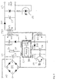
- a prior art switched mode supply as used in many appliances is schematically shown in Fig. 1. It comprises a bridge rectifier BR to which a mains voltage AC is coupled for providing a rectified voltage V1.
- the voltage V1 is coupled to an input capacitor C1 for smoothing the voltage V1 and is coupled to a first terminal 1 of a primary winding W1 of a transformer TR1.
- the primary winding W1 is coupled with its other end 2 to a switching transistor M1, which is coupled with a current output to ground.
- the switched mode power supply comprises in addition a driver circuit DR which is coupled to a control input of the switching transistor M1 for the operation of the switching transistor M1.
- the transformer TR1 comprises further a secondary winding W2 for providing a DC output voltage V2 via a rectifier diode D11 and a capacitor C3.
- the output voltage V2 is stabilized via a feedback circuit comprising an opto-coupler OK, which transmits a feedback signal Vfb to the primary side of the switched mode power supply to the driver stage DR.
- the driver stage includes for example a pulse-width modulator PWM for operating the switching transformer M1 in dependency of the current variation of a load.
- the switching transistor M1 is in this embodiment a MOSFET comprising a drain and a source terminal.
- the transformer TR1 comprises further an auxiliary winding W3 arranged on the primary side of the switched mode power supply, which is coupled to a supply circuit for generating a supply voltage Vcc during operation of the switch mode power supply.
- the supply circuit comprises a diode D13, which is coupled to the auxiliary winding W3, and a capacitor C4, which is coupled between an output terminal of the diode D13 and ground for providing a smoothed DC supply voltage VCC for the operation of the driver stage DR.
- the switched mode power supply comprises further a start-up circuit ST coupled to the input capacitor C1, which provides a start-up voltage Vstr for the driver stage DR, when the mains voltage AC is applied to the bridge rectifier BR.
- the start-up voltage Vstr is necessary for the driver stage DR for generating first switching pulses for the operation of the switching transistor M1.
- the nominal values of the voltages V2 and Vcc are reached for a normal mode operation of the switched mode power supply, in which the driver circuit DR uses the supply voltage Vcc for operation, and in which the start-up voltage Vstr is no more necessary.
- the driver circuit DR and the switching transistor M1 are integrated into an integrated controller circuit IC1, FSDH0265RN, manufactured by Fairchild Semiconductor Corporation.
- the controller circuit IC1 includes further parts of the start-up circuit for handling the voltage V1, in particular an internal switch, which switches from the start-up circuit ST to the supply voltage Vcc, when a supply voltage with a sufficiently high value is available after switching on of the power supply.
- the start up circuit ST comprises particularly a start-up resistor R4, which is coupled between the input capacitor C1 and an input terminal of the controller circuit IC1, and which has for example a value of 56 kOhm.
- a switched mode power supply of this kind it may happen that the input capacitor C1 is not discharged when the switched mode power supply is switched off.
- the capacitor C1 may keep a voltage which can stay above 100 Volts even for many days.
- a switched mode power supply of this kind provides therefore some danger for a user or even a qualified service person.
- the switched mode power supply comprises a transformer with a primary winding, a secondary winding and an auxiliary winding, a switching transistor coupled to the primary winding, a driver stage for the operation of the switching transistor, a supply circuit for providing a supply voltage for the operation of the driver stage, and an input capacitor coupled to a DC input voltage and to the primary winding. It comprises further a start-up circuit coupling the driver circuit to the input capacitor for providing a start-up current after switching on of the switched mode power supply, and a discharging circuit coupled to the supply voltage being provided by the supply circuit.
- the discharging circuit comprises in particular a switching stage, which is blocking during operation of the switched mode power supply, and which provides a current path for discharging the input capacitor, when the switched mode power supply is switched off.
- the discharging circuit is coupled with an input to an input voltage of the switched mode power supply for sensing, when an input voltage is present for the operation of the switched mode power supply.
- the switching stage switches through for discharging any charge capacitor of the supply circuit as well as the input capacitor.
- the start-up circuit comprises in particular a resistor with a high resistance, which is coupled to a supply voltage input of the driver circuit and therefore to the supply voltage of the supply circuit, which provides a smooth discharging of the input capacitor within a short time, when the switched mode power supply is switched off.
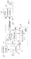
- the circuit arrangement as shown in figure 2 comprises a rectifier circuit BR for rectifying an AC mains voltage AC for a switched mode power supply comprising an input capacitor C1 and a switch mode transformer TR2, in correspondence with the switched mode power supply as described already before with regard to figure 1.
- the switched mode power supply comprises further a DC-DC converter which is coupled to an input voltage V1 at the input capacitor C1 via a start-up circuit comprising a resistor R4, for providing a start-up voltage for the start-up of the switched mode power supply, and comprises a supply circuit RE coupled to a switch mode transformer TR2 for providing a supply voltage Vcc during operation of the switched mode power supply.
- the circuit arrangement comprises further an AC power section AF arranged ahead of the rectifier circuit BR, which includes a mains filter.
- the switched mode power supply provides at the secondary side a DC output voltage V2 for the operation of a load L, and the switch mode transformer TR2 comprises further an auxiliary winding, not shown, for providing a voltage via diode D13 for the supply circuit RE during operation of the switched mode power supply.
- the DC-DC converter CO comprises in particular a driver stage and a switching transistor coupled to the primary winding of the switch mode transformer TR2, not shown.
- the DC-DC converter CO may comprise an integrated controller circuit as described with regard to figure 1.
- a switched mode power supply of this kind is known and corresponds essentially with that of figure 1, and may operate in particular, but not necessarily, as a flyback converter.
- the switched mode power supply comprises further a discharging circuit DI, which is coupled to the supply voltage Vcc via a node A. It comprises further an input terminal 3, which is coupled in this embodiment to a second input voltage V3 provided by the AC power section AF.
- the discharging circuit DI comprises a switching stage, in this embodiment a pnp transistor Q1, which is coupled with a current input via a resistor R3 to the node A and with a current output to ground.
- the control input of the switching stage is coupled to a diode D1 coupled to input terminal 3 for providing an operation of the switching stage in response to the AC mains voltage.
- the input terminal 3 may be coupled alternatively also to the rectifier circuit BR or to the input capacitor C1.
- a capacitor of the supply circuit RE is coupled, not shown, which provides the supply voltage Vcc for the DC-DC converter CO.
- the diode D1 provides a rectified voltage, which is applied via a voltage divider with resistors R1 and R2 to a charge capacitor C2.
- the capacitor C2 is coupled to the control input of the switching transistor Q1.
- a Zener diode ZD1 is coupled in parallel with the capacitor C2 for providing a threshold voltage for the operation of the switching stage with transistor Q1.
- the threshold voltage as defined by the Zener diode ZD1 is in particular such, that the voltage across capacitor C2, at node B, is higher than the supply voltage Vcc during operation of the switched mode power supply. This is the case also during a standby operation of the switched mode power supply.
- the operation of the switched mode power supply is as follows: When the mains voltage AC is applied to the circuit arrangement, after switching on of the arrangement, the input capacitor C1 is charged up via the rectifier circuit BR and a current is provided via resistor R4 of the start-up circuit for providing a supply voltage Vcc for the DC-DC converter CO. When the supply voltage Vcc reaches a threshold, the DC-DC converter CO starts operating and therefore the output voltages at the secondary winding and the auxiliary winding of the switch mode transformer TR2 are arising. After the start up phase, which may be in the range of about one second, the switched mode power supply goes into a normal operation mode, in which stabilized output voltages are present at the secondary winding and the auxiliary winding of the switch mode transformer TR2.
- the input voltage V3 is applied to the discharging circuit DI, which charges up the charge capacitor C2 via rectifier diode D1 and resistor R1, until the threshold as defined by the Zener diode ZD1 is reached.
- the capacitor C2 is charged up in a very short time and therefore the switching stage with transistor Q1 is blocked.
- the power consumption of the discharging circuit DE is therefore very low during operation of the switched mode power supply. This is also the case during the standby mode of the switched mode power supply.
- the voltage V3 is switched off also and therefore the charge capacitor C2 is discharged via resistor R2. Because at node A still the supply voltage Vcc is present, the switching stage switches through and as a result, any capacitor of the supply circuit RE is discharged and also the input capacitor C1 via the resistor R4 of the start-up circuit.
- the value of the resistor R3 can be selected such for example, that the input capacitor C1 is discharged within seconds.
- R1 200 kOhm
- R2 100 kOhm
- R3 1 kOhm
- R4 56 kOhm
- C1 330 micro-Farad
- C2 1 micro-Farad
- C4 47 micro-Farad
- Zener diode ZD1 with a nominal Zener voltage of 18 Volts.
Landscapes
- Engineering & Computer Science (AREA)
- Power Engineering (AREA)
- Dc-Dc Converters (AREA)
Priority Applications (1)
| Application Number | Priority Date | Filing Date | Title |
|---|---|---|---|
| EP06300123A EP1819032A1 (de) | 2006-02-10 | 2006-02-10 | Schaltnetzteil mit einer Entladevorrichtung |
Applications Claiming Priority (1)
| Application Number | Priority Date | Filing Date | Title |
|---|---|---|---|
| EP06300123A EP1819032A1 (de) | 2006-02-10 | 2006-02-10 | Schaltnetzteil mit einer Entladevorrichtung |
Publications (1)
| Publication Number | Publication Date |
|---|---|
| EP1819032A1 true EP1819032A1 (de) | 2007-08-15 |
Family
ID=36930201
Family Applications (1)
| Application Number | Title | Priority Date | Filing Date |
|---|---|---|---|
| EP06300123A Withdrawn EP1819032A1 (de) | 2006-02-10 | 2006-02-10 | Schaltnetzteil mit einer Entladevorrichtung |
Country Status (1)
| Country | Link |
|---|---|
| EP (1) | EP1819032A1 (de) |
Cited By (7)
| Publication number | Priority date | Publication date | Assignee | Title |
|---|---|---|---|---|
| WO2010003785A3 (en) * | 2008-07-11 | 2010-04-08 | Em Microelectronic-Marin Sa | Power supply unit having a voltage converter |
| CN101989810A (zh) * | 2009-07-31 | 2011-03-23 | 电力集成公司 | 用于实现功率转换器输入端电压放电电路的方法和装置 |
| WO2011119700A1 (en) | 2010-03-26 | 2011-09-29 | Cree, Inc. | Stored energy dissipating circuits and methods for switched mode power supplies |
| US8207577B2 (en) | 2009-09-29 | 2012-06-26 | Power Integrations, Inc. | High-voltage transistor structure with reduced gate capacitance |
| CN102904465A (zh) * | 2011-07-26 | 2013-01-30 | 罗姆股份有限公司 | Ac/dc转换器及使用其的ac电源适配器以及电子设备 |
| CN103580461A (zh) * | 2012-08-09 | 2014-02-12 | 艾默生网络能源有限公司 | 一种电源输出放电电路 |
| CN103683949A (zh) * | 2012-09-21 | 2014-03-26 | 三垦电气株式会社 | 开关电源装置 |
Citations (4)
| Publication number | Priority date | Publication date | Assignee | Title |
|---|---|---|---|---|
| JPS63209467A (ja) * | 1987-02-26 | 1988-08-31 | Meidensha Electric Mfg Co Ltd | スイツチング電源 |
| JPH07163142A (ja) * | 1993-11-30 | 1995-06-23 | Tec Corp | スイッチング電源 |
| JPH08149806A (ja) * | 1994-11-25 | 1996-06-07 | Mitsubishi Electric Corp | スイッチング電源回路 |
| US20050052886A1 (en) * | 2003-09-04 | 2005-03-10 | Ta-Yung Yang | Integrated start-up circuit with reduced power consumption |
-
2006
- 2006-02-10 EP EP06300123A patent/EP1819032A1/de not_active Withdrawn
Patent Citations (4)
| Publication number | Priority date | Publication date | Assignee | Title |
|---|---|---|---|---|
| JPS63209467A (ja) * | 1987-02-26 | 1988-08-31 | Meidensha Electric Mfg Co Ltd | スイツチング電源 |
| JPH07163142A (ja) * | 1993-11-30 | 1995-06-23 | Tec Corp | スイッチング電源 |
| JPH08149806A (ja) * | 1994-11-25 | 1996-06-07 | Mitsubishi Electric Corp | スイッチング電源回路 |
| US20050052886A1 (en) * | 2003-09-04 | 2005-03-10 | Ta-Yung Yang | Integrated start-up circuit with reduced power consumption |
Non-Patent Citations (3)
| Title |
|---|
| PATENT ABSTRACTS OF JAPAN vol. 012, no. 500 (E - 699) 27 December 1988 (1988-12-27) * |
| PATENT ABSTRACTS OF JAPAN vol. 1995, no. 09 31 October 1995 (1995-10-31) * |
| PATENT ABSTRACTS OF JAPAN vol. 1996, no. 10 31 October 1996 (1996-10-31) * |
Cited By (25)
| Publication number | Priority date | Publication date | Assignee | Title |
|---|---|---|---|---|
| US8446051B2 (en) | 2008-07-11 | 2013-05-21 | Em Microelectronic-Marin S.A. | Power supply unit having a voltage converter |
| TWI483513B (zh) * | 2008-07-11 | 2015-05-01 | Em Microelectronic Marin Sa | 裝備電源供應單元之電氣裝置 |
| CN102089957B (zh) * | 2008-07-11 | 2014-04-16 | Em微电子-马林有限公司 | 具有电压转换器的电力供给单元 |
| CN102089957A (zh) * | 2008-07-11 | 2011-06-08 | Em微电子-马林有限公司 | 具有电压转换器的电力供给单元 |
| WO2010003785A3 (en) * | 2008-07-11 | 2010-04-08 | Em Microelectronic-Marin Sa | Power supply unit having a voltage converter |
| JP2011527557A (ja) * | 2008-07-11 | 2011-10-27 | イーエム・ミクロエレクトロニク−マリン・エス アー | 電圧変換器を有する電源ユニット |
| US8159092B2 (en) | 2008-07-11 | 2012-04-17 | Em Microelectronic-Marin S.A. | Power supply unit having a voltage converter |
| US8624562B2 (en) | 2009-07-31 | 2014-01-07 | Power Integrations, Inc. | Method and apparatus for implementing a power converter input terminal voltage discharge circuit |
| EP2299571A1 (de) * | 2009-07-31 | 2011-03-23 | Power Integrations, Inc. | Verfahren und Vorrichtung zur Implementierung einer Spannungsablassschaltung eines Stromumwandlungseingabeendgeräts |
| US10153687B2 (en) | 2009-07-31 | 2018-12-11 | Power Integrations, Inc. | Method and apparatus for implementing a power converter input terminal voltage discharge circuit |
| US9735665B2 (en) | 2009-07-31 | 2017-08-15 | Power Integrations, Inc. | Method and apparatus for implementing a power converter input terminal voltage discharge circuit |
| EP2592738A3 (de) * | 2009-07-31 | 2014-01-29 | Power Integrations, Inc. | Verfahren und Vorrichtung zur Implementierung einer Spannungsablassschaltung eines Stromumwandlungseingabeendgeräts |
| US9065340B2 (en) | 2009-07-31 | 2015-06-23 | Power Integrations, Inc. | Method and apparatus for implementing a power converter input terminal voltage discharge circuit |
| US10608525B2 (en) | 2009-07-31 | 2020-03-31 | Power Integrations, Inc. | Method and apparatus for implementing a power converter input terminal voltage discharge circuit |
| CN101989810A (zh) * | 2009-07-31 | 2011-03-23 | 电力集成公司 | 用于实现功率转换器输入端电压放电电路的方法和装置 |
| CN104242631A (zh) * | 2009-07-31 | 2014-12-24 | 电力集成公司 | 用于实现功率转换器输入端电压放电电路的方法和装置 |
| US8207577B2 (en) | 2009-09-29 | 2012-06-26 | Power Integrations, Inc. | High-voltage transistor structure with reduced gate capacitance |
| WO2011119700A1 (en) | 2010-03-26 | 2011-09-29 | Cree, Inc. | Stored energy dissipating circuits and methods for switched mode power supplies |
| EP2553787A4 (de) * | 2010-03-26 | 2017-12-27 | Cree, Inc. | Schaltkreise zur abschwächung gespeicherter energie und verfahren für schaltmodus-netzteile |
| CN102904465A (zh) * | 2011-07-26 | 2013-01-30 | 罗姆股份有限公司 | Ac/dc转换器及使用其的ac电源适配器以及电子设备 |
| CN102904465B (zh) * | 2011-07-26 | 2017-03-01 | 罗姆股份有限公司 | Ac/dc转换器及使用其的ac电源适配器以及电子设备 |
| CN103580461A (zh) * | 2012-08-09 | 2014-02-12 | 艾默生网络能源有限公司 | 一种电源输出放电电路 |
| CN103580461B (zh) * | 2012-08-09 | 2016-03-30 | 艾默生网络能源有限公司 | 一种电源输出放电电路 |
| CN103683949B (zh) * | 2012-09-21 | 2016-03-30 | 三垦电气株式会社 | 开关电源装置 |
| CN103683949A (zh) * | 2012-09-21 | 2014-03-26 | 三垦电气株式会社 | 开关电源装置 |
Similar Documents
| Publication | Publication Date | Title |
|---|---|---|
| EP1642381B1 (de) | Schaltnetzteil | |
| JP3495012B2 (ja) | スイッチング電源装置 | |
| US5661642A (en) | Switching power supply | |
| JP5253304B2 (ja) | エネルギ伝達エレメントの入力にわたる電圧から導かれた電流に応答するための回路および方法 | |
| JP5494009B2 (ja) | スイッチング制御回路及びスイッチング電源装置 | |
| CN111092552A (zh) | 开关电源控制用半导体装置和ac-dc变换器 | |
| EP1675252A1 (de) | Vorrichtung zur Pulsbreitenmodulationssteuerung mit Standby-Modus | |
| US20060209581A1 (en) | Terminal for multiple functions in a power supply | |
| JP4289904B2 (ja) | Ac−dcコンバータ | |
| US20070086223A1 (en) | Dc-dc converter | |
| KR20170119683A (ko) | 전원 제어용 반도체 장치 | |
| CN110401347B (zh) | 直流电源装置 | |
| KR20170118729A (ko) | 전원 제어용 반도체 장치 | |
| KR100703821B1 (ko) | 스위칭 파워 서플라이 | |
| JP7775647B2 (ja) | 集積回路及び電源回路 | |
| CN101218737A (zh) | 用于开关模式电源的反馈通信技术 | |
| KR101677731B1 (ko) | 자동 재 시작 회로 및 그 방법 | |
| JP2010063293A (ja) | 省電力電源装置 | |
| CN100440696C (zh) | 切换式电源 | |
| JPH11235037A (ja) | 自励発振型スイッチング電源装置 | |
| JP2004201436A (ja) | Dc−dcコンバータにおける出力電流の逆流抑制回路、dc−dcコンバータの自励発振時保護回路、及びdc−dcコンバータの自励発振保護回路 | |
| JP2006254691A (ja) | スイッチング電源におけるスイッチ用の制御回路 | |
| JP4680453B2 (ja) | スイッチング電源 | |
| JP3763273B2 (ja) | スイッチング電源 | |
| JP2004222472A (ja) | スイッチング電源制御回路 |
Legal Events
| Date | Code | Title | Description |
|---|---|---|---|
| PUAI | Public reference made under article 153(3) epc to a published international application that has entered the european phase |
Free format text: ORIGINAL CODE: 0009012 |
|
| AK | Designated contracting states |
Kind code of ref document: A1 Designated state(s): AT BE BG CH CY CZ DE DK EE ES FI FR GB GR HU IE IS IT LI LT LU LV MC NL PL PT RO SE SI SK TR |
|
| AX | Request for extension of the european patent |
Extension state: AL BA HR MK YU |
|
| AKX | Designation fees paid | ||
| STAA | Information on the status of an ep patent application or granted ep patent |
Free format text: STATUS: THE APPLICATION IS DEEMED TO BE WITHDRAWN |
|
| 18D | Application deemed to be withdrawn |
Effective date: 20080216 |
|
| REG | Reference to a national code |
Ref country code: DE Ref legal event code: 8566 |