EP1821110A2 - Vorrichtung zum kontaktlosen Testen von elektrischen Verbindungen - Google Patents
Vorrichtung zum kontaktlosen Testen von elektrischen Verbindungen Download PDFInfo
- Publication number
- EP1821110A2 EP1821110A2 EP07101085A EP07101085A EP1821110A2 EP 1821110 A2 EP1821110 A2 EP 1821110A2 EP 07101085 A EP07101085 A EP 07101085A EP 07101085 A EP07101085 A EP 07101085A EP 1821110 A2 EP1821110 A2 EP 1821110A2
- Authority
- EP
- European Patent Office
- Prior art keywords
- conductor
- electrode
- electrons
- electrodes
- potential
- Prior art date
- Legal status (The legal status is an assumption and is not a legal conclusion. Google has not performed a legal analysis and makes no representation as to the accuracy of the status listed.)
- Withdrawn
Links
Images

Classifications
-
- G—PHYSICS
- G01—MEASURING; TESTING
- G01R—MEASURING ELECTRIC VARIABLES; MEASURING MAGNETIC VARIABLES
- G01R31/00—Arrangements for testing electric properties; Arrangements for locating electric faults; Arrangements for electrical testing characterised by what is being tested not provided for elsewhere
- G01R31/28—Testing of electronic circuits, e.g. by signal tracer
- G01R31/302—Contactless testing
- G01R31/305—Contactless testing using electron beams
Definitions
- the invention relates to the non-contact testing of electrical characteristics of electronic components, such as insulation between conductors, electrical continuity of conductors, resistance, and even capacitance and inductance.
- the test is non-contact in the sense that an injection or an extraction of electrons in the conductors to be tested is obtained by an effect of tearing electrons under the influence of an electromagnetic beam (in principle a ray beam ultraviolet) having a photon energy greater than the energy of extracting an electron from the conductor.
- an electromagnetic beam in principle a ray beam ultraviolet
- Non-contact test devices are mainly intended to verify the electrical interconnections in interconnection supports such as printed circuits or, especially, support substrates of integrated circuits (in English "chip-carriers") with very large numbers of output terminals.
- interconnection supports such as printed circuits or, especially, support substrates of integrated circuits (in English "chip-carriers") with very large numbers of output terminals.
- a interconnect substrate (“chip-carrier”) is interposed, having hundreds of very dense contact pads on the side which receives an integrated circuit chip with a very large number of contacts, and having an often fewer number of contact pads on the back, the side to be soldered on the printed circuit board.
- test points on the back side in the form of a so-called “nail bed”, ie an addressable contact tip matrix, because the density of contact is weaker, it is almost impossible to do it on the side that carries the chip.
- Non-contact test systems have therefore been developed to allow testing of the interconnect substrate from the side that carries the chip. The test can also be done in a mixed way with test points (or other access mode by direct contact) on the back less dense, and a contactless test on the front more dense.
- Non-contact test devices have already been proposed capable of either extracting electrons from a conductor to be tested, or injecting electrons into this conductor, or finally performing an extraction operation and an injection operation simultaneously. on two portions of conductor to test the isolation, continuity, or resistance between these two portions.
- the patent application WO 01/38892 the patent US 4,573,008 , describe such devices.
- the electrodes are arranged in the form of a matrix array of rows and columns of small individual elementary electrodes, isolated from each other. other and selectively addressable to be individually carried to a desired potential is negative or positive depending on whether to extract electrons or inject electrons.
- the collection and emission electrodes are then formed in exactly the same way, but they play a role of collection or emission according to the potential to which they are brought. In the following we will speak only of collection electrodes for simplicity, knowing that they play indifferently the role of collection or emission, and will be called collection plate plate that carries the network of addressable electrodes.
- each individual collection electrode In order to measure the insulation or electrical continuity characteristics of the conductors of the substrate, each individual collection electrode also has a measuring capacitance.
- the measuring capacitance serves both to maintain for a certain time a bias voltage of the collection electrode and to store the electric charges displaced at the time of the extraction or injection of electrons, for a reading of these charges (later or simultaneously).
- the measurement capacitance may initially be brought to a reference potential and in a second step be connected to a charge reading circuit; the load reading circuit will measure the possible loss of load due to an insulation fault between two points.
- the addressing circuit comprises buses of one or more line conductors, buses of one or more column conductors, and, locally near each individual electrode, a circuitry of a few transistors connected to these buses; the buses and transistors are deposited in thin layer (so-called TFT transistors of the English “thin-film transistors”) on the plate which is both electrically insulating and transparent to electromagnetic radiation (in principle ultraviolet rays) used.
- the electrode array and the circuitry associated with each electrode, capacitance, transistors and conductive connections occupy an important place on the collection plate.
- the electromagnetic beam that is used to bombard either an electrode or a conductor of the test substrate is applied through the collection plate because the electromagnetic source can not be placed in the narrow gap between the collection plate and the substrate to be tested. If the substrate to be tested is below the collection plate, then the radiation source is located above the plate. The elements present on the collection plate therefore impair the transparency of the plate and hinder the passage of the beam to the driver to load or unload.
- the electrodes are made in the form of a perforated conductive grid.
- the capacitance associated with each individual electrode is provided by a first armature constituted by the electrode itself, in the form of a perforated conductive grid, and by a second armature constituted by another grid. perforated conductor, located below the first gate and separated from it by a layer of dielectric material.
- a non-contact test device for a substrate comprising conductive connections
- the device comprising a collection plate provided with an array of individual electrodes each associated with a local capacitor and provided with circuits for addressing a chosen electrode and the capacitance associated with desired potentials and / or for measuring the potential of the electrodes or capacitance, and an electromagnetic illumination source capable of illuminating a point region of a conductive connection of the substrate to carry out an electron extraction of this zone or an injection of electrons in this zone, each individual electrode being made in the form of a perforated conductive grid, a first reinforcement of the capacity comprising the perforated grid, and a second reinforcement of the capacity comprising a second perforated conductive grid located opposite the first gate and separated from it by a layer of dielectric material.
- the transparency of the collection plate is maximized vis-à-vis the illumination beam, without reducing the value of the capacity.
- the extraction of electrons from a conductive connection of the substrate to be tested is preferably by direct illumination of this connection through the collection plate, the potential of at least one collection electrode vis-à-vis the illuminated point area being more positive than that of the connection.
- the injection of electrons is preferably done by illumination of this conductive connection through the collection plate, reflection of the beam on the connection to at least one collection electrode, and extraction of electrons from this electrode by the reflected beam, the potential of the reflection-illuminated electrode being more negative than the potential of the illuminated conductive connection.
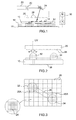
- the substrate to be tested is designated by the reference 10; it is for example a multilayer interconnection substrate of type known as "chip carrier", with multiple interconnections between a rear face (bottom in the figure) and a front face (top in the figure).
- the back side is intended to be soldered on a printed circuit and the front face is intended to receive an integrated circuit chip.
- the connections of the back face are designated by 12. They mainly comprise solder pads for directly soldering the substrate on a printed circuit.
- the connections of the front face, which are denser than those of the rear face, are designated by 14. These connections 14 mainly comprise contact pads, or solder pads, making it possible to connect this range by direct soldering to an output terminal.
- an integrated circuit chip (a "flip-chip” type of welding, that is to say a chip turned face-up against its support).
- a flip-chip type of welding, that is to say a chip turned face-up against its support.
- conductors, or conductive connections or welding pads or contact pads it being understood that the test envisaged is intended to test in a general manner n Any electrical conductor accessible by these faces, but most often we will perform the test on contact pads.
- the contact pads or solder pads of the front face each comprise, for example, an indium solder ball.
- an addressing network 16 has been represented making it possible to establish an electrical connection by contact. direct or indirect physics with a welding range 12 of the rear face.
- the addressing network 16 may be connected to the rear face contact pads via a contact sheet 18 constituted either by a bed of test points or by a single layer with anisotropic conduction: this layer with anisotropic conduction establishes an electrical current connection in the vertical direction (transverse to the layer) but not in the horizontal direction, so that if a network conductor 16 is supplied with voltage, this voltage will be applied to a contact pad 12 located above this conductor, but not to other contact pads. It is thus possible, for a test involving a conductor of the rear face, to apply a desired potential by addressing this conductor from the network 16, and to read a current flowing through this conductor during the test.
- the test On the side of the front face, the test is contactless: a source of electromagnetic radiation 20, preferably ultraviolet light, associated with a focusing optics 22 and a reflection optic 24 (for example a directional mirror controlled), directs a narrow brush on a selected point area of a driver to be tested.
- the test machine is programmatically controlled to successively illuminate, by appropriate control of the mirror, the thousands of points which are generally to be tested in an interconnect substrate.
- the energy of the radiation pulls electrons from the driver. These electrons are attracted by a collection plate 26 brought to a potential more positive than the potential of the illuminated conductor.
- the driver thus charges a positive potential as the electrons are extracted, just as if a current were circulated in the conductor.
- the current can be measured at this stage or at a later stage, or the potential of the conductor can be measured at this stage or at a later stage.
- the collection plate 26 is placed in close proximity to the substrate to be tested, to avoid having to apply potentials that are too high to produce the electric field that will attract the electrons to the collection plate.
- the gap between the substrate and the plate is a high vacuum interval, so that the electrons flow freely.
- the collection plate is placed between the ultraviolet radiation source and the substrate to be tested. It is partly transparent to the radiation, that is to say that its surface is not entirely occupied by the collection electrodes.
- each electrode is, for example, a few tens of micrometers apart and the collection plate may comprise an array of several hundred in-line electrodes and several hundred column electrodes.
- in-line and column addressing it is possible to carry one or more collection electrodes, located in front of a substrate conductor to be positively charged, to a positive potential; the neighboring collection electrodes may even be brought to a negative potential to repel the electrons that could be directed towards them.
- the addressing means of the collection electrodes are not shown.
- the collection electrodes are each constituted in the form of a perforated grid. This is not shown in Figure 1 given the scale of the drawing.
- the beam ultraviolet light can also indirectly bombard an individual collection electrode, charged to a more negative potential than the driver to be tested. This extracts electrons from the electrode and these electrons are attracted to the driver to be tested, thereby providing an electron injection into the conductor.
- Indirect bombardment involves reflecting a portion of the ultraviolet beam on the conductor to be tested, the reflected radiation itself bombarding a collection electrode located immediately vis-à-vis. The conductor of the substrate, placed at a potential more negative than the electrode which emitted the electrons, collects the latter.
- the addressing circuits of the collection electrodes and the addressing circuits of the conductors at the rear of the interconnect substrate are not shown.
- a current measurement circuit circulating between a conductor of the rear face and a conductor of the front face of the interconnection substrate is represented symbolically. But it is also possible to measure the current between two conductors of the front panel, or to store in a capacitance a charge that has elapsed during an electron injection or an electron extraction and then read the stored charge.
- FIGS. 2 and 3 show more realistically a substrate portion 10 to be tested with, on the front face of the substrate, two conductors in the form of two solder pads each comprising a solder ball 32 and 34 respectively ( indium balls or others).
- the left conductor 32 is connected to a conductor 36 of the rear face of the substrate, so that it is possible to choose the potential to which it is carried by the addressing network 16 of Figure 1.
- the driver right 34 n It is not connected to a back-side conductor and it is through the ultraviolet beam that it is injected or extracted electrons. This figure shows that it is possible, by extracting electrons from the contact pad 32, to verify that this stud is well connected to the rear-face conductor 36, simply by measuring the current flowing in the measuring circuit 30 of FIG.
- Figure 3 is a top view showing both the configuration of the two contact pads 32 and 34 with their balls and the configuration of the electrode array 28 checkerboard, vis-à-vis these pads.
- An individual electrode corresponds to a square of the checkerboard and each individual electrode can be brought to a potential selected independently of the potential of the other electrodes.
- each individual electrode is shown as being solid to simplify the figure.
- each electrode is constituted in the form of a perforated conductive grid because of the need for a radiation transparency of the source 20.
- the electrode board appears to cover practically the entire surface of the electrode. the collection plate.
- the electrodes occupy only a part of this surface: line conductors and column conductors must be inserted between the horizontal and vertical rows of electrodes, and each individual electrode is associated locally with a switching circuit. a few transistors that allows both the selection of an individual electrode (at the intersection of a row and a column of the network) and the choice of a potential to be applied to this electrode.
- this capacity comprises two frames, one of which is the electrode itself in the form of a perforated grid and the other is also a perforated grid located below the electrode and facing it.
- FIG. 3 makes it possible to understand how potentials will be applied to the collection electrodes, as a function of their position with respect to the point-like conductive zones in which electrons are to be injected or extracted: for extracting electrons, for example from the conductive pad 32, whose surface represents some adjacent electrodes, one will carry the few individual electrodes that are opposite this pad to a positive potential; here are four electrodes represented in gray and designated by the overall reference 28A; the electrodes surrounding them may remain at zero potential or even be brought to a negative potential; conversely, to inject electrons, the electrodes would be brought to a negative potential, and the surrounding electrodes would be left at a zero or even positive potential; for example four electrodes generally designated 28B and placed opposite the conductive pad 34 can be brought to a negative potential. For example, it is possible to test the desirable or undesirable presence, or the characteristics, of a conductive path between the pads 32 and 34, represented symbolically under the reference 38 in FIG.
- FIG. 4 shows schematically the electrical circuitry which corresponds to what has just been described. Only two rows and two columns of electrodes have been represented, ie four individual electrodes in all.
- the electrodes are designated 281 and 282 for the first line, 283 and 284 for the second line. They are drawn in the form of a checkerboard to signify that they are constituted by openwork grids. Behind each electrode is shown a second capacity frame, respectively 481, 482, 483, 484. This second frame is not shown in the form of a checkerboard to avoid confusing the drawing, but it is well constituted by a perforated grid design identical to that of the collection electrode.
- the two grids are electrically separated by a dielectric layer not shown in FIG.
- FIG. 4 shows an ADL line addressing circuit which controls the conductors of the line buses in order to make the transistors connected to a selected conductor simultaneously conductive, and an ACM addressing and measuring circuit which selects the conductors of the column bus to apply potentials or to read potentials or circulations of electric charges.
- a general controller CG controls the overall operation of all the circuitry present on the collection plate 26.
- FIG. 5 makes it possible to understand how the measuring capacitance is achieved by the superposition of two openwork grids separated by a dielectric layer.
- the collection plate is for example a glass plate 50 on which are formed, by deposition techniques and thin film etching, both the electrodes, the capacitance, the individual switching circuits, the conductors of the line buses and column, and possibly other circuit elements.
- FIG. 5 there is shown two adjacent electrodes 281 and 282 and the corresponding capacity plates 481 and 482 and it was assumed for simplicity that the openwork grids have only three bars each.
- the collecting plate 26 comprises, for example, an electrically insulating support which is transparent to ultraviolet rays, for example a glass plate 50.
- a glass plate 50 On this glass plate are successively deposited and etched a conductive layer 52 constituting the reinforcements 481 and 482 of the capacitor, a dielectric layer 54, and a conductive layer 56 constituting the collection electrodes 281, 282 which themselves constitute the other armature capabilities.
- the conductive layers 52 and 56 can be made of metal (aluminum, copper, tungsten or metal alloy for example) etched in the form of a perforated grid.
- the dielectric layer 54 may be of oxide or silicon nitride, for example).
- the etching of the two conductive layers is such that the grid-shaped collection electrode openwork comes exactly above the first perforated grid remaining separated from it by the dielectric layer.
- the two conductive layers may be made of the same material. In the perforated zones, there is no obstacle to the passage of ultraviolet radiation, so that a large fraction of the ultraviolet beam can pass through the plate to reach a conductor of the substrate to be tested below the plate.
- the other circuit elements are placed: transistors and conductors of lines and columns. These elements are located in zones designated 58 in FIG. 5. These zones may be small in size since they have no measurement capacity.
- the two armatures of the capacitor are connected, by the switches of the switching circuit, to column conductors.
- test device In an example of use of the test device according to the invention, it is possible to test the isolation between two conductors of the front face of the interconnection substrate.
- the following process is given only as an example.
- the conductors to be tested have a reference potential (mass potential for example), which can be done by conventional means such as a carbon brush rubbed on the front face of the substrate to be tested.
- a reference potential mass potential for example
- the following operations are then carried out: the first conductor is taken to a positive potential Vp by ejecting electrons from this conductor by direct ultraviolet illumination through the collection plate, a first collection electrode (at least) located opposite the first conductor, being brought to a positive potential and the neighboring electrodes remaining at a zero or negative potential.
- the second conductor is applied to the same positive potential Vp by injecting electrons into this conductor by direct ultraviolet illumination of the second conductor, at least one collection electrode located opposite the second conductor being brought to a positive potential, the others to a negative potential.
- Vp the positive potential
- the amount of charge that flows from the collection electrode to the second conductor is measured. If it is equal to a reference value obtained by prior calibration, this means that at the time of the second illumination, the second driver was still at the reference potential and he was not influenced by the positive potential. from the first driver.
- the quantity of charges is lower than this reference value, or even if it is zero, it is because the potential of the second conductor has increased under the influence of the charge of the first conductor, showing an insulation fault. between the two drivers.
- the potential chosen, and the amount of charge measured a leakage resistance between the conductors can be determined and whether the interconnect substrate is to be considered defective.
- the electrical continuity between two conductors of the front face of the substrate is tested.
- This operation assumes that two ultraviolet sources are available to illuminate the two conductors separately.
- the first conductor is charged to a positive potential Vp relative to the reference potential, and the second to a negative potential.
- the positive charge is made by direct illumination of the first conductor, at least a first collection electrode, above the conductor, being brought to a positive potential, and the surrounding electrodes being at a negative potential.
- the negative charge is by indirect illumination of a collection electrode located above the second conductor and brought to a negative potential (the surrounding electrodes being at a positive potential); indirect illumination is by reflection of the ultraviolet beam on the second conductor.
- the charges of electrons circulating in the electrodes during this double illumination are measured for the first electrode and the second electrode.
- Load analysis compared to calibration charts, provides information on the electrical resistance present between the first and second conductors.
Landscapes
- Engineering & Computer Science (AREA)
- General Engineering & Computer Science (AREA)
- Physics & Mathematics (AREA)
- General Physics & Mathematics (AREA)
- Tests Of Electronic Circuits (AREA)
- Measuring Leads Or Probes (AREA)
Applications Claiming Priority (1)
| Application Number | Priority Date | Filing Date | Title |
|---|---|---|---|
| FR0601385A FR2897690B1 (fr) | 2006-02-17 | 2006-02-17 | Dispositif de test de connexions electriques, sans contact |
Publications (2)
| Publication Number | Publication Date |
|---|---|
| EP1821110A2 true EP1821110A2 (de) | 2007-08-22 |
| EP1821110A3 EP1821110A3 (de) | 2012-06-27 |
Family
ID=37074658
Family Applications (1)
| Application Number | Title | Priority Date | Filing Date |
|---|---|---|---|
| EP07101085A Withdrawn EP1821110A3 (de) | 2006-02-17 | 2007-01-24 | Vorrichtung zum kontaktlosen Testen von elektrischen Verbindungen |
Country Status (4)
| Country | Link |
|---|---|
| US (1) | US7446543B2 (de) |
| EP (1) | EP1821110A3 (de) |
| JP (1) | JP2007218919A (de) |
| FR (1) | FR2897690B1 (de) |
Cited By (2)
| Publication number | Priority date | Publication date | Assignee | Title |
|---|---|---|---|---|
| CN104931869A (zh) * | 2014-08-29 | 2015-09-23 | 杭州广立微电子有限公司 | 可寻址环形振荡器测试芯片 |
| CN107860780A (zh) * | 2017-10-12 | 2018-03-30 | 彩虹集团(邵阳)特种玻璃有限公司咸阳分公司 | 一种玻璃缺陷变形量的检测装置及方法 |
Families Citing this family (3)
| Publication number | Priority date | Publication date | Assignee | Title |
|---|---|---|---|---|
| FR2920590B1 (fr) * | 2007-08-28 | 2009-11-20 | New Imaging Technologies Sas | Pixel actif cmos a tres grande dynamique de fonctionnement |
| US10689754B2 (en) * | 2017-09-05 | 2020-06-23 | Peter C. Salmon | Programmable charge storage arrays and associated manufacturing devices and systems |
| CN116296858B (zh) * | 2023-05-26 | 2023-08-04 | 常州市双佳电器有限公司 | 一种led灯防爆检测装置 |
Family Cites Families (5)
| Publication number | Priority date | Publication date | Assignee | Title |
|---|---|---|---|---|
| DE2902495A1 (de) * | 1979-01-23 | 1980-07-31 | Siemens Ag | Einrichtung zur beruehrungslosen potentialmessung |
| JPS55156867A (en) * | 1979-05-28 | 1980-12-06 | Hitachi Ltd | Potential measuring device |
| JPH065691B2 (ja) * | 1987-09-26 | 1994-01-19 | 株式会社東芝 | 半導体素子の試験方法および試験装置 |
| US5404110A (en) * | 1993-03-25 | 1995-04-04 | International Business Machines Corporation | System using induced current for contactless testing of wiring networks |
| FR2801680B3 (fr) * | 1999-11-26 | 2002-02-15 | Christophe Vaucher | Methode de test electrique de la conformite de l'interconnexion de conducteurs electriques disposes sur un substrat, sans contact et sans outillage |
-
2006
- 2006-02-17 FR FR0601385A patent/FR2897690B1/fr not_active Expired - Fee Related
-
2007
- 2007-01-24 EP EP07101085A patent/EP1821110A3/de not_active Withdrawn
- 2007-02-16 US US11/675,934 patent/US7446543B2/en not_active Expired - Fee Related
- 2007-02-16 JP JP2007036498A patent/JP2007218919A/ja active Pending
Cited By (3)
| Publication number | Priority date | Publication date | Assignee | Title |
|---|---|---|---|---|
| CN104931869A (zh) * | 2014-08-29 | 2015-09-23 | 杭州广立微电子有限公司 | 可寻址环形振荡器测试芯片 |
| CN104931869B (zh) * | 2014-08-29 | 2018-06-19 | 杭州广立微电子有限公司 | 可寻址环形振荡器测试芯片 |
| CN107860780A (zh) * | 2017-10-12 | 2018-03-30 | 彩虹集团(邵阳)特种玻璃有限公司咸阳分公司 | 一种玻璃缺陷变形量的检测装置及方法 |
Also Published As
| Publication number | Publication date |
|---|---|
| FR2897690B1 (fr) | 2008-04-18 |
| FR2897690A1 (fr) | 2007-08-24 |
| US20070194310A1 (en) | 2007-08-23 |
| US7446543B2 (en) | 2008-11-04 |
| JP2007218919A (ja) | 2007-08-30 |
| EP1821110A3 (de) | 2012-06-27 |
Similar Documents
| Publication | Publication Date | Title |
|---|---|---|
| EP0606805B1 (de) | Testverfahren für Elemente von integrierten Schaltungen und dazugehöriges integriertes Element | |
| US4443278A (en) | Inspection of multilayer ceramic circuit modules by electrical inspection of green specimens | |
| EP1821110A2 (de) | Vorrichtung zum kontaktlosen Testen von elektrischen Verbindungen | |
| US5216359A (en) | Electro-optical method and apparatus for testing integrated circuits | |
| EP1236052B1 (de) | Elektrische prüfung der verbindung von leitern auf einem substrat | |
| JPH0614085B2 (ja) | 導電経路のテスト方法 | |
| FR2554622A1 (fr) | Procede de fabrication d'une matrice de composants electroniques | |
| EP0245147A1 (de) | Röntgen-Bilderfassungstafel und deren Herstellungsverfahren | |
| FR2604014A1 (fr) | Dispositif de conversion de l'information comportant des lignes auxiliaires d'adresses afin d'ameliorer le rendement de fabrication | |
| JP2017502484A (ja) | 検査、テスト、デバッグ、及び表面の改変のための電子ビーム誘導プラズマプローブの適用 | |
| FR2709375A1 (fr) | Dispositif d'affichage d'images et circuit de commande associé. | |
| FR2697673A1 (fr) | Circuit à fusible, pour circuit intégré. | |
| DE10016996C1 (de) | Testanordnung zur Funktionsprüfung eines Halbleiterchips | |
| EP2076925B1 (de) | Einrichtung zum elektromagnetischen koppeln eines elektromagnetischen strahlungssensors | |
| EP0908944A1 (de) | Elektrische Kennzeichnung einer Isolierschicht, die ein leitendes oder halbleitendes Substrat bedeckt | |
| FR2617977A1 (fr) | Appareil de test de circuit imprime | |
| Jhabvala et al. | Development and operation of the microshutter array system | |
| US20080018349A1 (en) | Method for testing electrical elements using an indirect photoelectric effect | |
| US20080006427A1 (en) | Method and System for Testing or Measuring Electrical Elements, Using Two Offset Pulses | |
| Nagayoshi et al. | Development of a Large-Format X-Ray Microcalorimeter Array Based on a Ti/Au Transition-Edge Sensor | |
| EP0102296B1 (de) | Verfahren zum Herstellen einer Matrix aus elektronischen Komponenten | |
| EP1953823A1 (de) | ESD-Schutz für Integrierte Schaltungen | |
| FR2565354A1 (fr) | Procede et dispositif de test de circuits integres sur tranches | |
| FR2635414A1 (en) | Optical switching device and applications to circuit testing | |
| WO2006082292A1 (fr) | Procede et systeme de test ou de mesure d'elements electriques |
Legal Events
| Date | Code | Title | Description |
|---|---|---|---|
| PUAI | Public reference made under article 153(3) epc to a published international application that has entered the european phase |
Free format text: ORIGINAL CODE: 0009012 |
|
| AK | Designated contracting states |
Kind code of ref document: A2 Designated state(s): AT BE BG CH CY CZ DE DK EE ES FI FR GB GR HU IE IS IT LI LT LU LV MC NL PL PT RO SE SI SK TR |
|
| AX | Request for extension of the european patent |
Extension state: AL BA HR MK YU |
|
| RAP1 | Party data changed (applicant data changed or rights of an application transferred) |
Owner name: COMMISSARIAT A L'ENERGIE ATOMIQUE ET AUX ENERGIES |
|
| PUAL | Search report despatched |
Free format text: ORIGINAL CODE: 0009013 |
|
| AK | Designated contracting states |
Kind code of ref document: A3 Designated state(s): AT BE BG CH CY CZ DE DK EE ES FI FR GB GR HU IE IS IT LI LT LU LV MC NL PL PT RO SE SI SK TR |
|
| AX | Request for extension of the european patent |
Extension state: AL BA HR MK RS |
|
| RIC1 | Information provided on ipc code assigned before grant |
Ipc: G01R 31/305 20060101AFI20120522BHEP |
|
| 17P | Request for examination filed |
Effective date: 20121123 |
|
| AKX | Designation fees paid |
Designated state(s): AT BE BG CH CY CZ DE DK EE ES FI FR GB GR HU IE IS IT LI LT LU LV MC NL PL PT RO SE SI SK TR |
|
| GRAP | Despatch of communication of intention to grant a patent |
Free format text: ORIGINAL CODE: EPIDOSNIGR1 |
|
| INTG | Intention to grant announced |
Effective date: 20140710 |
|
| STAA | Information on the status of an ep patent application or granted ep patent |
Free format text: STATUS: THE APPLICATION IS DEEMED TO BE WITHDRAWN |
|
| 18D | Application deemed to be withdrawn |
Effective date: 20140801 |