EP0908944A1 - Elektrische Kennzeichnung einer Isolierschicht, die ein leitendes oder halbleitendes Substrat bedeckt - Google Patents
Elektrische Kennzeichnung einer Isolierschicht, die ein leitendes oder halbleitendes Substrat bedeckt Download PDFInfo
- Publication number
- EP0908944A1 EP0908944A1 EP19980402488 EP98402488A EP0908944A1 EP 0908944 A1 EP0908944 A1 EP 0908944A1 EP 19980402488 EP19980402488 EP 19980402488 EP 98402488 A EP98402488 A EP 98402488A EP 0908944 A1 EP0908944 A1 EP 0908944A1
- Authority
- EP
- European Patent Office
- Prior art keywords
- insulating layer
- electrical
- face
- electrodes
- electrode
- Prior art date
- Legal status (The legal status is an assumption and is not a legal conclusion. Google has not performed a legal analysis and makes no representation as to the accuracy of the status listed.)
- Granted
Links
Images


Classifications
-
- G—PHYSICS
- G01—MEASURING; TESTING
- G01R—MEASURING ELECTRIC VARIABLES; MEASURING MAGNETIC VARIABLES
- G01R31/00—Arrangements for testing electric properties; Arrangements for locating electric faults; Arrangements for electrical testing characterised by what is being tested not provided for elsewhere
- G01R31/12—Testing dielectric strength or breakdown voltage ; Testing or monitoring effectiveness or level of insulation, e.g. of a cable or of an apparatus, for example using partial discharge measurements; Electrostatic testing
- G01R31/1227—Testing dielectric strength or breakdown voltage ; Testing or monitoring effectiveness or level of insulation, e.g. of a cable or of an apparatus, for example using partial discharge measurements; Electrostatic testing of components, parts or materials
- G01R31/1263—Testing dielectric strength or breakdown voltage ; Testing or monitoring effectiveness or level of insulation, e.g. of a cable or of an apparatus, for example using partial discharge measurements; Electrostatic testing of components, parts or materials of solid or fluid materials, e.g. insulation films, bulk material; of semiconductors or LV electronic components or parts; of cable, line or wire insulation
- G01R31/129—Testing dielectric strength or breakdown voltage ; Testing or monitoring effectiveness or level of insulation, e.g. of a cable or of an apparatus, for example using partial discharge measurements; Electrostatic testing of components, parts or materials of solid or fluid materials, e.g. insulation films, bulk material; of semiconductors or LV electronic components or parts; of cable, line or wire insulation of components or parts made of semiconducting materials; of LV components or parts
-
- H—ELECTRICITY
- H10—SEMICONDUCTOR DEVICES; ELECTRIC SOLID-STATE DEVICES NOT OTHERWISE PROVIDED FOR
- H10P—GENERIC PROCESSES OR APPARATUS FOR THE MANUFACTURE OR TREATMENT OF DEVICES COVERED BY CLASS H10
- H10P74/00—Testing or measuring during manufacture or treatment of wafers, substrates or devices
- H10P74/20—Testing or measuring during manufacture or treatment of wafers, substrates or devices characterised by the properties tested or measured, e.g. structural or electrical properties
- H10P74/207—Electrical properties, e.g. testing or measuring of resistance, deep levels or capacitance-voltage characteristics
-
- H—ELECTRICITY
- H10—SEMICONDUCTOR DEVICES; ELECTRIC SOLID-STATE DEVICES NOT OTHERWISE PROVIDED FOR
- H10P—GENERIC PROCESSES OR APPARATUS FOR THE MANUFACTURE OR TREATMENT OF DEVICES COVERED BY CLASS H10
- H10P74/00—Testing or measuring during manufacture or treatment of wafers, substrates or devices
- H10P74/27—Structural arrangements therefor
- H10P74/277—Circuits for electrically characterising or monitoring manufacturing processes, e.g. circuits in tested chips or circuits in testing wafers
-
- H—ELECTRICITY
- H10—SEMICONDUCTOR DEVICES; ELECTRIC SOLID-STATE DEVICES NOT OTHERWISE PROVIDED FOR
- H10W—GENERIC PACKAGES, INTERCONNECTIONS, CONNECTORS OR OTHER CONSTRUCTIONAL DETAILS OF DEVICES COVERED BY CLASS H10
- H10W72/00—Interconnections or connectors in packages
- H10W72/071—Connecting or disconnecting
- H10W72/075—Connecting or disconnecting of bond wires
- H10W72/07551—Connecting or disconnecting of bond wires characterised by changes in properties of the bond wires during the connecting
- H10W72/07553—Connecting or disconnecting of bond wires characterised by changes in properties of the bond wires during the connecting changes in shapes
-
- H—ELECTRICITY
- H10—SEMICONDUCTOR DEVICES; ELECTRIC SOLID-STATE DEVICES NOT OTHERWISE PROVIDED FOR
- H10W—GENERIC PACKAGES, INTERCONNECTIONS, CONNECTORS OR OTHER CONSTRUCTIONAL DETAILS OF DEVICES COVERED BY CLASS H10
- H10W72/00—Interconnections or connectors in packages
- H10W72/20—Bump connectors, e.g. solder bumps or copper pillars; Dummy bumps; Thermal bumps
- H10W72/29—Bond pads specially adapted therefor
-
- H—ELECTRICITY
- H10—SEMICONDUCTOR DEVICES; ELECTRIC SOLID-STATE DEVICES NOT OTHERWISE PROVIDED FOR
- H10W—GENERIC PACKAGES, INTERCONNECTIONS, CONNECTORS OR OTHER CONSTRUCTIONAL DETAILS OF DEVICES COVERED BY CLASS H10
- H10W72/00—Interconnections or connectors in packages
- H10W72/50—Bond wires
- H10W72/531—Shapes of wire connectors
-
- H—ELECTRICITY
- H10—SEMICONDUCTOR DEVICES; ELECTRIC SOLID-STATE DEVICES NOT OTHERWISE PROVIDED FOR
- H10W—GENERIC PACKAGES, INTERCONNECTIONS, CONNECTORS OR OTHER CONSTRUCTIONAL DETAILS OF DEVICES COVERED BY CLASS H10
- H10W72/00—Interconnections or connectors in packages
- H10W72/50—Bond wires
- H10W72/531—Shapes of wire connectors
- H10W72/536—Shapes of wire connectors the connected ends being ball-shaped
-
- H—ELECTRICITY
- H10—SEMICONDUCTOR DEVICES; ELECTRIC SOLID-STATE DEVICES NOT OTHERWISE PROVIDED FOR
- H10W—GENERIC PACKAGES, INTERCONNECTIONS, CONNECTORS OR OTHER CONSTRUCTIONAL DETAILS OF DEVICES COVERED BY CLASS H10
- H10W72/00—Interconnections or connectors in packages
- H10W72/50—Bond wires
- H10W72/59—Bond pads specially adapted therefor
-
- H—ELECTRICITY
- H10—SEMICONDUCTOR DEVICES; ELECTRIC SOLID-STATE DEVICES NOT OTHERWISE PROVIDED FOR
- H10W—GENERIC PACKAGES, INTERCONNECTIONS, CONNECTORS OR OTHER CONSTRUCTIONAL DETAILS OF DEVICES COVERED BY CLASS H10
- H10W72/00—Interconnections or connectors in packages
- H10W72/90—Bond pads, in general
- H10W72/931—Shapes of bond pads
- H10W72/934—Cross-sectional shape, i.e. in side view
-
- H—ELECTRICITY
- H10—SEMICONDUCTOR DEVICES; ELECTRIC SOLID-STATE DEVICES NOT OTHERWISE PROVIDED FOR
- H10W—GENERIC PACKAGES, INTERCONNECTIONS, CONNECTORS OR OTHER CONSTRUCTIONAL DETAILS OF DEVICES COVERED BY CLASS H10
- H10W72/00—Interconnections or connectors in packages
- H10W72/90—Bond pads, in general
- H10W72/951—Materials of bond pads
Definitions
- the present invention relates to a method of electrical characterization of an insulating layer covering a conductive or semiconductor substrate. It also relates to a device for setting work of this characterization process.
- the gate oxide is an essential part of MOS integrated circuits (Metal Oxide Semiconductor). The quality of this oxide very much depends on the starting semiconductor substrate.
- a known method for achieving this result consists in depositing a layer of oxide (called thin oxide thereafter) of the same type as desired grid on one side (or front side) of a control substrate and electrically test this oxide thin between a front contact and a rear contact.
- the rear contact is usually a platter metallic conductive placed on the rear side of the control substrate.
- the manufacture of the front contact must not degrade the thin oxide deposited on the face front of the substrate.
- This front contact has an area of given contact which defines the portion of oxide tested.
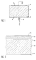
- Figure 1 illustrates the principle work applied to a coated silicon substrate 1 a layer of silica 2 on its front face 3.
- the contact with the rear face 4 of the substrate 1 is produced by a metal plate 5 connected to ground.
- the front contact, with the free face of the thin oxide 2 is produced by a mercury electrode 6 which allows to apply a voltage V compared to the mass.
- the simplest test is to detect major faults, i.e. short circuits thin oxide premises. These short circuits are by example due to outgrowth of silicon making protruding from the substrate.
- the test takes place in walking the mercury electrode on the free face of thin oxide 2. If the front contact is placed on a portion of oxide containing a major defect, we measure a leakage current I from low values of the voltage V.
- V bd breakdown voltage of the thin oxide in the portion of oxide tested.
- the insulating layer was arranged on a semiconductor material forming a substrate whose rear face received contact back.
- a test proves impossible to perform in some cases, for example on an SOI substrate (silicon on insulator) as shown in Figure 2.
- This substrate comprises a mass 10 of silicon, constituting the initial substrate and having a face rear 11.
- oxide layer 12 On the opposite side, we increased oxide layer 12, called buried oxide layer, then a silicon layer 13 is reported.
- This SOI substrate thus formed is then covered with a layer thin oxide 14, called thin oxide, which must be tested.
- the buried oxide 12 opposing the current flow between the thin oxide 14 and the face rear 11 even if a defect exists in the portion of thin oxide tested.
- a first method would be to keep thin oxide over the entire surface of the substrate. In this case, a large current I would only be measured if the thin oxide has a defect in each of the two oxide portions contacted. A defect present in one of the two portions would not be detected if the other portion of oxide was intact.
- a second method would be to eliminate locally thin oxide so as to lay one of the two front contacts on the silicon film. That represents a technological step, which can degrade the thin oxide to be tested. In addition, it is very difficult to distinguish optically the areas covered with oxide thin and uncovered areas because the thin oxide is practically transparent. The positioning of contacts would therefore be tricky.
- this invention proposes a solution whose basic principle is the next.
- a major defect forming short circuit under one of the contacts of the measured.
- Major defect can be obtained by application of a sufficiently high electrical voltage to achieve a breakdown of the insulating layer. This electrical voltage can be applied by through two electrodes brought into contact electric with the second side of the insulating layer, thus creating two major defects in the layer insulation, one or both of these major faults used to apply the electrical test.
- Major defect can still be obtained mechanically, by crossing the insulating layer.
- the major fault can be created in an area of annular shape centered on the layer area insulation to be tested.
- the electrical test consists of applying an electrical voltage between said electrodes and take any current flowing between said electrodes. Electric voltage applied between the electrodes can then be a voltage ramp.
- a particularly interesting application of the invention relates to a semiconductor substrate comprising a buried insulating layer and a layer surface insulator which is the insulating layer to test.
- This semiconductor substrate can in particular be a substrate called Silicon-On-Insulator where the layer buried is a layer of silicon oxide and where the surface insulating layer is also a layer silicon oxide.
- silicon underlying the surface oxide layer is maintained under strong illumination during application of the electrical test in order to favor the generation of minority holders.
- Another way to promote generation of minority carriers involves wearing the silicon underlying the oxide layer superficial at a temperature above the room temperature during test application electric.
- the device can include at least three electrodes suitable for being brought into contact with the second side of the insulating layer, two of these electrodes for applying a breakdown voltage to the insulating layer to create two defects major, the third electrode serving, with one at less than the other two electrodes, to apply said electrical test.
- the means to create at least one major defect can also be mechanical means operating by crossing of the insulating layer.
- the electrode used jointly to apply the breakdown voltage and the electrical test can have an annular contact area, the electrode suitable for being brought into contact with the area to be tested being centered on the annular contact area.
- Electrical test application electrodes can be mercury electrodes.
- the means for applying the test electrical supply an electrical signal in the form of ramp between the major fault and said area to be tested.
- the means to apply the test electric include means for accessing to the measurement of the current that can flow between the electrodes allowing the application of the electrical test.
- Figure 3 illustrates the process according to the present invention in the case of the substrate shown in FIG. 2.
- the characterization device used comprises a mercury probe with three or more contacts.
- the face rear 11 is grounded using an electrode plate 20.
- the face of the thin oxide opposite the face which is in contact with the silicon layer 13 and which has a thickness between 3 and 1000 nm, is put in contact with three mercury electrodes 21, 22 and 23.
- the electrode 21 is grounded, the electrode 22 is left at a floating potential and a high voltage V 3 is applied to the electrode 23, for example - 100 V.
- V 3 a high voltage
- the current I 3 is for example greater than 1 mA.
- V 2 breakdown voltage
- the front face of the substrate is maintained under strong lighting during the setting process work.
- the purpose of this enlightenment is to maximize the current in major faults which can be described simply as junctions Schottky mercury-silicon.
- junctions Schottky mercury-silicon When such a junction is polarized live, it does not oppose current flow. However, when it is reverse polarized, it only lets one pass low current called leakage current. The light promotes the generation of minority carriers and maximizes the leakage current in the junction (s) which are in reverse.
- Another solution to maximize the current in major faults is to increase the temperature at the level of major faults under the electrodes 21 and 23.
- the illumination of the substrate on the front face side can be done without problem if the substrate holder, in which the vertical mercury channels for the electrodes 21, 22 and 23 are pierced, is made of transparent material.
- the illumination must be strong enough to increase the leakage current significantly. You can use a 100 W halogen lamp (white) focused on less than 1 cm 2 .
- FIGS. 4, 5 and 6 give examples of results obtained on different SOI substrates. These diagrams show on the ordinate the current I 2 in nA and on the abscissa the voltage V 2 in volts.
- FIG. 4 presents results obtained for a thin oxide 15 nm thick covering an SOI substrate, the underlying silicon having n-type doping at the rate of 10 17 atoms / cm 3 .
- Curve 41 is representative of intact sites.
- Curve 42 corresponds to a site presenting a major defect.
- FIG. 5 presents results obtained for a thin oxide 7.5 nm thick covering an SOI substrate, the underlying silicon not being doped.
- Curve 51 is representative of intact sites.
- Curves 52 and 53 correspond to sites with a major defect.
- FIG. 6 presents results obtained for a thin oxide 15 nm thick covering an SOI substrate, the underlying silicon not being doped.
- Curve 61 is representative of intact sites.
- Curves 62 and 63 correspond to sites with a major defect.
- the method according to the invention applies to SOI substrates doped or not.
- the doped substrates give larger currents on the defective oxide portions because the film of silicon underlying the oxide is less resistive.
- the method according to the invention can be extended to characterization devices (or probes) having more than three mercury electrodes. Each electrode additional test a portion of more in each site. For example, a four probe mercury electrodes can test the thin oxide in two servings. If in addition these two contacts are of different surfaces, we can do studies of defectiveness depending on the test surface.
- the shape of the mercury electrodes does not have a decisive importance.
- An interesting possibility is to give the electrode used to create the fault middle finger the shape of a ring surrounding the test area.
- Figure 7 shows such an arrangement. We find, concentrically arranged a test electrode central 71, a first electrode 72 to obtain a first major fault by breakdown and a second electrode 73 to obtain a second major fault by slamming.
- the method according to the present invention can be implemented using conductive contacts solids (metal studs, polymer deposits conductors), obtained depending on the case by evaporation, filing and engraving, or by any other method not degrading the thin oxide to be tested.
- conductive contacts solids metal studs, polymer deposits conductors
- the cost and time of making these contacts drivers can be a barrier to their implementation artwork.
- the insulating layer to be characterized may have a free face or be covered with a structure providing electrical access to this layer like the shows figure 8.
- This figure shows a very detailed enlarged of a substrate under characterization.
- the substrate 80 has a conductive part 81 or semiconductor covered with an insulating layer 82 with variations in thickness.
- the insulating layer 82 may be a layer of silicon oxide comprising relatively thin portions 83 separated by portions 84 of thick LOCOS type oxide more important.
- portions 83, and between portions 84 are arranged conductive pads 85, for example in polycrystalline silicon.
- the electrodes of the characterization device for example the mercury electrode 22, can then provide a electrical contact with portions 83 of low thickness of the oxide layer through the conductive studs 85.
- the invention is of course applicable to other substrates as SOI substrates, for example at SiC substrates on insulator.
- the present invention lends itself to different execution variants.
- the same electrode can be used to form several major defects, which allows a higher current to flow.
- the electrical test may consist of applying a AC voltage to the area to be tested and, from the measurement of the alternating current flowing, to be determined the impedance of the insulating layer (e.g. layer of silicon oxide) and the underlying material (for example silicon) by analysis of its phase and its amplitude.
- the quality of the oxide can be expressed in the form of a resistance and capacity measure, conductance and capacitance, self and resistance, of self and impedance.
- a voltage varying along a ramp, along a staircase or in an impulse can be applied to the area to be tested.
- Another higher voltage is applied and the current and duration required to obtain zero voltage are measured and so on.
- We can then determine the breakdown load Q bd ⁇ Ixt.
- the electrical test can be carried out by measuring the current flowing between the electrodes. Instead of making a current measurement, one can make a voltage measurement. The voltage can be controlled so that the current obtained remains constant. The time at the end of which the oxide breaks down is noted and the current product X time is calculated to determine Q bd which is the charge spent in the oxide during this time. The value of Q bd makes it possible to characterize the oxide.
Landscapes
- Physics & Mathematics (AREA)
- General Physics & Mathematics (AREA)
- Testing Or Measuring Of Semiconductors Or The Like (AREA)
Applications Claiming Priority (2)
| Application Number | Priority Date | Filing Date | Title |
|---|---|---|---|
| FR9712604A FR2769753B1 (fr) | 1997-10-09 | 1997-10-09 | Caracterisation electrique d'une couche isolante recouvrant un substrat conducteur ou semiconducteur |
| FR9712604 | 1997-10-09 |
Publications (2)
| Publication Number | Publication Date |
|---|---|
| EP0908944A1 true EP0908944A1 (de) | 1999-04-14 |
| EP0908944B1 EP0908944B1 (de) | 2011-11-30 |
Family
ID=9512015
Family Applications (1)
| Application Number | Title | Priority Date | Filing Date |
|---|---|---|---|
| EP19980402488 Expired - Lifetime EP0908944B1 (de) | 1997-10-09 | 1998-10-07 | Elektrische Charakterisierung einer Isolierschicht, die ein leitendes oder halbleitendes Substrat bedeckt |
Country Status (3)
| Country | Link |
|---|---|
| US (1) | US6074886A (de) |
| EP (1) | EP0908944B1 (de) |
| FR (1) | FR2769753B1 (de) |
Cited By (1)
| Publication number | Priority date | Publication date | Assignee | Title |
|---|---|---|---|---|
| WO2008099316A1 (en) | 2007-02-13 | 2008-08-21 | Philips Intellectual Property & Standards Gmbh | Defect treatment apparatus |
Families Citing this family (6)
| Publication number | Priority date | Publication date | Assignee | Title |
|---|---|---|---|---|
| US6528335B2 (en) * | 2001-02-14 | 2003-03-04 | International Business Machines Corporation | Electrical method for assessing yield-limiting asperities in silicon-on-insulator wafers |
| US6458634B1 (en) * | 2001-04-18 | 2002-10-01 | International Business Machines Corporation | Reduction of induced charge in SOI devices during focused ion beam processing |
| US7011980B1 (en) * | 2005-05-09 | 2006-03-14 | International Business Machines Corporation | Method and structures for measuring gate tunneling leakage parameters of field effect transistors |
| WO2009133501A1 (en) * | 2008-04-29 | 2009-11-05 | Philips Intellectual Property & Standards Gmbh | Oled device with current limiting layer |
| US20120212245A1 (en) * | 2011-02-22 | 2012-08-23 | Qualcomm Incorporated | Circuit and method for testing insulating material |
| CN113702450B (zh) * | 2020-05-22 | 2024-08-30 | 金风科技股份有限公司 | 磁极覆层缺陷的检测方法及装置 |
Citations (4)
| Publication number | Priority date | Publication date | Assignee | Title |
|---|---|---|---|---|
| JPS63142826A (ja) * | 1986-12-05 | 1988-06-15 | Tokyo Electron Ltd | プロ−ブカ−ド |
| JPH02275364A (ja) * | 1989-04-15 | 1990-11-09 | Matsushita Electric Works Ltd | 抵抗測定装置 |
| EP0581703A1 (de) * | 1992-07-30 | 1994-02-02 | STMicroelectronics S.A. | Verfahren zur Prüfung des Schichtwiderstandes einer Diffusionsschicht |
| WO1996023319A2 (en) * | 1995-01-20 | 1996-08-01 | Vlsi Technology, Inc. | Wafer level prediction of thin oxide reliability |
Family Cites Families (2)
| Publication number | Priority date | Publication date | Assignee | Title |
|---|---|---|---|---|
| US5907764A (en) * | 1995-11-13 | 1999-05-25 | Advanced Micro Devices, Inc. | In-line detection and assessment of net charge in PECVD silicon dioxide (oxide) layers |
| US6014034A (en) * | 1996-10-24 | 2000-01-11 | Texas Instruments Incorporated | Method for testing semiconductor thin gate oxide |
-
1997
- 1997-10-09 FR FR9712604A patent/FR2769753B1/fr not_active Expired - Fee Related
-
1998
- 1998-09-17 US US09/156,127 patent/US6074886A/en not_active Expired - Lifetime
- 1998-10-07 EP EP19980402488 patent/EP0908944B1/de not_active Expired - Lifetime
Patent Citations (4)
| Publication number | Priority date | Publication date | Assignee | Title |
|---|---|---|---|---|
| JPS63142826A (ja) * | 1986-12-05 | 1988-06-15 | Tokyo Electron Ltd | プロ−ブカ−ド |
| JPH02275364A (ja) * | 1989-04-15 | 1990-11-09 | Matsushita Electric Works Ltd | 抵抗測定装置 |
| EP0581703A1 (de) * | 1992-07-30 | 1994-02-02 | STMicroelectronics S.A. | Verfahren zur Prüfung des Schichtwiderstandes einer Diffusionsschicht |
| WO1996023319A2 (en) * | 1995-01-20 | 1996-08-01 | Vlsi Technology, Inc. | Wafer level prediction of thin oxide reliability |
Non-Patent Citations (4)
| Title |
|---|
| "CHARACTERIZING WEAK SPOTS IN DIELECTRIC LAYERS", IBM TECHNICAL DISCLOSURE BULLETIN, vol. 34, no. 4B, 1 September 1991 (1991-09-01), pages 98 - 99, XP000189506 * |
| PATENT ABSTRACTS OF JAPAN vol. 012, no. 402 (E - 673) 25 October 1988 (1988-10-25) * |
| PATENT ABSTRACTS OF JAPAN vol. 015, no. 037 (P - 1159) 29 January 1991 (1991-01-29) * |
| WANG H ET AL: "AN OPTIMIZED GATE OXIDE BREAKDOWN TEST BY ACTIVATING OXIDE TRAPS ATLOW FIELDS", INTERNATIONAL ELECTRON DEVICES MEETING 1992, SAN FRANCISCO, DEC. 13 - 16, 1992, 13 December 1992 (1992-12-13), INSITUTE OF ELECTRICAL AND ELECTRONICS ENGINEERS, pages 143 - 146, XP000687397 * |
Cited By (1)
| Publication number | Priority date | Publication date | Assignee | Title |
|---|---|---|---|---|
| WO2008099316A1 (en) | 2007-02-13 | 2008-08-21 | Philips Intellectual Property & Standards Gmbh | Defect treatment apparatus |
Also Published As
| Publication number | Publication date |
|---|---|
| EP0908944B1 (de) | 2011-11-30 |
| FR2769753A1 (fr) | 1999-04-16 |
| US6074886A (en) | 2000-06-13 |
| FR2769753B1 (fr) | 1999-12-03 |
Similar Documents
| Publication | Publication Date | Title |
|---|---|---|
| EP1236052B1 (de) | Elektrische prüfung der verbindung von leitern auf einem substrat | |
| FR2998419A1 (fr) | Protection d'un circuit integre contre des attaques | |
| EP0908944B1 (de) | Elektrische Charakterisierung einer Isolierschicht, die ein leitendes oder halbleitendes Substrat bedeckt | |
| Brovko et al. | Effects of oxygen plasma treatment on Cd1− xZnxTe material and devices | |
| US5138256A (en) | Method and apparatus for determining the thickness of an interfacial polysilicon/silicon oxide film | |
| EP2076925A1 (de) | Einrichtung zum elektromagnetischen koppeln eines elektromagnetischen strahlungssensors | |
| US5976898A (en) | Localization of defects of a metallic layer of a semiconductor circuit | |
| FR2694410A1 (fr) | Procédé de test de la résistance par carré de couches diffusées. | |
| US6528335B2 (en) | Electrical method for assessing yield-limiting asperities in silicon-on-insulator wafers | |
| FR2726691A1 (fr) | Photodetecteur de grande dimension et procede de realisation d'un tel photodetecteur | |
| EP1821110A2 (de) | Vorrichtung zum kontaktlosen Testen von elektrischen Verbindungen | |
| EP0053213A1 (de) | Vierpolkondensator, dessen Integrität mit Hilfe eines Gleichstromtests kontrolliert werden kann | |
| FR2786569A1 (fr) | Circuit de test de cellules eeprom | |
| EP3739622A1 (de) | Verfahren zur erfassung der möglichen verletzung der integrität eines halbleitersubstrats eines integrierten schaltkreises von seiner rückseite aus, und entsprechender integrierter schaltkreis | |
| US7291508B2 (en) | Laser probe points | |
| Lanir et al. | Ebic characterization of HgCdTe crystals and photodiodes | |
| FR2656158A1 (fr) | Photosenseur hybride. | |
| EP0108676B1 (de) | Messvorrichtung für sehr schwache Ströme | |
| ZIMMERMANN | Measurement of Spatial Variations of the | |
| JP2005331241A (ja) | 導電性試料の評価方法及び導電性試料の評価装置 | |
| FR3149740A1 (fr) | Procede de caracterisation electrique d’un materiau absorbeur sous illumination variable | |
| Giordana et al. | Front contact electroreflectance: An alternative technique for semiconductor optical studies | |
| JPH06112290A (ja) | 半導体評価装置 | |
| JPH05259251A (ja) | 配線の信頼性評価用パターンと配線の信頼性評価方法 | |
| FR3160809A1 (fr) | Véhicule de test et méthode de test pour des dispositifs microélectroniques |
Legal Events
| Date | Code | Title | Description |
|---|---|---|---|
| PUAI | Public reference made under article 153(3) epc to a published international application that has entered the european phase |
Free format text: ORIGINAL CODE: 0009012 |
|
| AK | Designated contracting states |
Kind code of ref document: A1 Designated state(s): DE GB IT |
|
| AX | Request for extension of the european patent |
Free format text: AL;LT;LV;MK;RO;SI |
|
| RTI1 | Title (correction) | ||
| 17P | Request for examination filed |
Effective date: 19990916 |
|
| AKX | Designation fees paid |
Free format text: DE GB IT |
|
| RAP1 | Party data changed (applicant data changed or rights of an application transferred) |
Owner name: COMMISSARIAT A L'ENERGIE ATOMIQUE |
|
| 17Q | First examination report despatched |
Effective date: 20080118 |
|
| RAP1 | Party data changed (applicant data changed or rights of an application transferred) |
Owner name: COMMISSARIAT A L'ENERGIE ATOMIQUE ET AUX ENERGIES |
|
| GRAP | Despatch of communication of intention to grant a patent |
Free format text: ORIGINAL CODE: EPIDOSNIGR1 |
|
| GRAS | Grant fee paid |
Free format text: ORIGINAL CODE: EPIDOSNIGR3 |
|
| GRAA | (expected) grant |
Free format text: ORIGINAL CODE: 0009210 |
|
| AK | Designated contracting states |
Kind code of ref document: B1 Designated state(s): DE GB IT |
|
| REG | Reference to a national code |
Ref country code: GB Ref legal event code: FG4D Free format text: NOT ENGLISH |
|
| REG | Reference to a national code |
Ref country code: DE Ref legal event code: R096 Ref document number: 69842518 Country of ref document: DE Effective date: 20120301 |
|
| PG25 | Lapsed in a contracting state [announced via postgrant information from national office to epo] |
Ref country code: IT Free format text: LAPSE BECAUSE OF FAILURE TO SUBMIT A TRANSLATION OF THE DESCRIPTION OR TO PAY THE FEE WITHIN THE PRESCRIBED TIME-LIMIT Effective date: 20111130 |
|
| PLBE | No opposition filed within time limit |
Free format text: ORIGINAL CODE: 0009261 |
|
| STAA | Information on the status of an ep patent application or granted ep patent |
Free format text: STATUS: NO OPPOSITION FILED WITHIN TIME LIMIT |
|
| 26N | No opposition filed |
Effective date: 20120831 |
|
| REG | Reference to a national code |
Ref country code: DE Ref legal event code: R097 Ref document number: 69842518 Country of ref document: DE Effective date: 20120831 |
|
| GBPC | Gb: european patent ceased through non-payment of renewal fee |
Effective date: 20121007 |
|
| PG25 | Lapsed in a contracting state [announced via postgrant information from national office to epo] |
Ref country code: DE Free format text: LAPSE BECAUSE OF NON-PAYMENT OF DUE FEES Effective date: 20130501 Ref country code: GB Free format text: LAPSE BECAUSE OF NON-PAYMENT OF DUE FEES Effective date: 20121007 |
|
| REG | Reference to a national code |
Ref country code: DE Ref legal event code: R119 Ref document number: 69842518 Country of ref document: DE Effective date: 20130501 |