EP1829351B1 - Isolation de signaux d'emission et de reception - Google Patents
Isolation de signaux d'emission et de reception Download PDFInfo
- Publication number
- EP1829351B1 EP1829351B1 EP05852480.2A EP05852480A EP1829351B1 EP 1829351 B1 EP1829351 B1 EP 1829351B1 EP 05852480 A EP05852480 A EP 05852480A EP 1829351 B1 EP1829351 B1 EP 1829351B1
- Authority
- EP
- European Patent Office
- Prior art keywords
- signal
- channel
- filter
- unit
- impedance
- Prior art date
- Legal status (The legal status is an assumption and is not a legal conclusion. Google has not performed a legal analysis and makes no representation as to the accuracy of the status listed.)
- Expired - Lifetime
Links
Images






Classifications
-
- H—ELECTRICITY
- H04—ELECTRIC COMMUNICATION TECHNIQUE
- H04B—TRANSMISSION
- H04B1/00—Details of transmission systems, not covered by a single one of groups H04B3/00 - H04B13/00; Details of transmission systems not characterised by the medium used for transmission
- H04B1/38—Transceivers, i.e. devices in which transmitter and receiver form a structural unit and in which at least one part is used for functions of transmitting and receiving
- H04B1/40—Circuits
- H04B1/50—Circuits using different frequencies for the two directions of communication
- H04B1/52—Hybrid arrangements, i.e. arrangements for transition from single-path two-direction transmission to single-direction transmission on each of two paths or vice versa
- H04B1/525—Hybrid arrangements, i.e. arrangements for transition from single-path two-direction transmission to single-direction transmission on each of two paths or vice versa with means for reducing leakage of transmitter signal into the receiver
-
- H—ELECTRICITY
- H04—ELECTRIC COMMUNICATION TECHNIQUE
- H04B—TRANSMISSION
- H04B1/00—Details of transmission systems, not covered by a single one of groups H04B3/00 - H04B13/00; Details of transmission systems not characterised by the medium used for transmission
- H04B1/38—Transceivers, i.e. devices in which transmitter and receiver form a structural unit and in which at least one part is used for functions of transmitting and receiving
- H04B1/40—Circuits
- H04B1/54—Circuits using the same frequency for two directions of communication
- H04B1/58—Hybrid arrangements, i.e. arrangements for transition from single-path two-direction transmission to single-direction transmission on each of two paths or vice versa
- H04B1/583—Hybrid arrangements, i.e. arrangements for transition from single-path two-direction transmission to single-direction transmission on each of two paths or vice versa using a bridge network
-
- H—ELECTRICITY
- H04—ELECTRIC COMMUNICATION TECHNIQUE
- H04B—TRANSMISSION
- H04B3/00—Line transmission systems
- H04B3/02—Details
- H04B3/03—Hybrid circuits
Definitions
- the invention relates to communication devices and, in particular, to a method and apparatus for isolating transmitted and received signals.
- Full-duplex operation provides the advantage of maximizing channel utilization because data may be simultaneously transmitted and received over the same path.
- the channel may comprise one or more conductors or paths, that each may simultaneously carry transmit and receive signals.
- full-duplex operation provides the advantage of simultaneous use of the channel for transmission and reception
- full-duplex operation must acquire a low level incoming (receive) signal, while concurrently sending the outgoing (transmit) signal at an appropriate power level.
- the power level of the incoming signal may be one or more orders of magnitude less than the power level of the outgoing signal.
- a voltage source 104 receives an outgoing transmit signal on a transmit port 108.
- the voltage source 104 has low output impedance, shown as R out .
- the output of the voltage source 104 connects to resistors R S and R 1 .
- the opposing terminal of resistor R S connects to a channel port 110 and a positive input terminal of a low noise amplifier 112, which is configured for a voltage differencing operation.
- the negative input terminal of the amplifier 112 connects to the opposing terminal of resistor R 1 and through resistor R 2 to ground.
- a resistor R L represents the impedance of the channel.
- a signal transmitted by the voltage source 104 is provided to the channel through a resistor R S .
- the amount of attenuation occurring as a result of R S is determined by the channel impedance R L and is defined as the loss in the outgoing path of the hybrid.
- Receive signals are represented as the difference between the positive and negative input terminals of the differencing amplifier 112.
- the operation of a hybrid is generally understood and hence, not discussed in detail beyond the following.
- the circuit directs the transmit signal to resistors R S and R 1 .
- the circuit configuration of this prior art hybrid directs the transmit signal to both the positive and negative input terminals of the differencing amplifier 112. By properly selecting the values for R 1 and R 2 , generally equal transmit signal levels are provided to the inputs of the differencing amplifier thereby canceling the transmit signal. This in turn removes the transmit signal from the receive signal.
- the receive signal With regard to the receive signal, it is provided directly to the positive input of the differencing amplifier, with resistor R S providing a termination impedance in series with R out .
- the voltage source 104 appears as an AC virtual ground to the incoming receive signal, and consequently, no receive signal appears at the negative input of the differencing amplifier 112. While this configuration proved satisfactory for prior art systems and applications, its utility in wideband communication systems is hindered by the bandwidth limitations of the voltage source 104.
- the system shown in Figure 1 the voltage source 104 must be cable of operating at frequencies many times greater than the bandwidth of the incoming signal.
- the output impedance of the voltage source 104 starts to increase at frequencies many times lower than the signal bandwidth of the voltage source thereby impeding circuit operation. High-frequency operation may require use of an ultra-high bandwidth voltage source, with up to potentially 10 times the bandwidth of the incoming signal, and use of such a device is inefficient with respect to power dissipation and cost.
- a replica hybrid circuit is similar to the embodiment shown in Figure 1 , except it employs two driver amplifiers (voltage or current): a primary driver amplifier that generates the outgoing signal and a secondary driver amplifier that generates a replica of the transmit signal used to remove the outgoing signal from the receive signal. If the noise and distortion characteristics of the replica signal do not match the noise and distortion characteristics of the primary outgoing signal, then this approach suffers from an unacceptable level of noise and distortion at the output of the differencing amplifier 112. This approach generally requires driver amplifiers that have very low distortion and very low noise because distortion and noise from the primary driver amplifier does not perfectly match the distortion and noise of the replica driver amplifier, and consequently, transmit noise and distortion are not significantly attenuated at the differencing amplifier output.
- Diplexers are likewise not well suited to wideband applications.
- a diplexer enables full-duplex operation over a single channel by separating the channel into frequency bands for exclusive use by the incoming and outgoing signals.
- Using a diplexer can provide adequate isolation if high-order high pass and low-pass filters are used to separate the incoming and outgoing signals, but because certain portions of the channel bandwidth are reserved for incoming signals and certain portions of the channel bandwidth are reserved for outgoing signals, the full capacity of the channel is not utilized. This is an unacceptable solution for a wide-bandwidth communication system designed to meet high data transmit rate requirements over a narrowband channel.
- directional devices such as active or passive circulators, power splitters, or directional couplers
- such devices may be configured to provide adequate isolation, but suffer from the drawback of an unacceptably large degree of incoming signal or outgoing signal attenuation, an inadequate degree of wideband isolation, or a combination of these drawbacks.
- the directional device may be configured to provide adequate wideband isolation, but generally only at the expense of incoming signal attenuation, outgoing signal attenuation, or both.
- a passive circulator adequate isolation can only be realized over a narrow band of operation.
- use of directional devices for wideband, high data rate applications over bandlimited channels is generally not feasible.
- EP 1 081 874 discloses a hybrid circuit forming an interface between a transmission line and heads of transmission-reception of signals in bands of different frequencies in transmission and reception, including a line transformer, and means for separating bands combined with echo cancellation means.
- a first aspect of the present invention provides a method as claimed in Claim 1.
- the first filter and the second filter have a generally identical frequency responses and the filtering may comprise phase shifting and attenuating one or more signals.
- the channel comprises one or more twisted pair conductors.
- the first filter and the second filter are configured to generate an all-pass (i.e., flat magnitude) frequency response for the isolation circuit.
- the differencing device comprises a differencing amplifier. It is contemplated that the processing of the outgoing signal may comprise performing first processing on the outgoing signal and performing second processing on the outgoing signal. The processing may be performed by one or more filters and at least one of the one or more filters may comprise an attenuator and a delay.
- the isolation circuit may further comprise a termination impedance, connected to the second filter, configured to match the impedance of the channel.
- the first filter and the second filter may each comprise a delay and an attenuator.
- the isolation circuit may have a lead-lag frequency response that produces high-frequency pre-emphasis.
- the transfer function of the signal isolation unit is frequency dependant and that the transfer function of the signal isolation unit is optimized for the communications channel.
- the transfer function of the signal isolation unit is an all-pass function. This unit may further comprise a termination impedance.
- the signal isolation unit is configured in a differential mode. In one mode of operation, each input of the differencing amplifier receives a generally identical filtered version of a signal received on the transmit port.
- At least one filter comprises at least one delay and at least one attenuator.
- an isolation circuit may be associated with each differential path.
- a termination impedance is provided which has an impedance value related to the channel impedance.
- a variable filter, a variable termination impedance, or both allow the receive signal transfer function (frequency response) and characteristic impedance of the tuned isolation circuit to be dynamically adjusted to complement the characteristics of the channel.
- the pertinent channel characteristics may be derived from a channel estimation circuit, located at the receive port, in this embodiment the third port. In other embodiments other systems or methods may be used to determine or estimate the channel characteristics.
- the channel estimation circuit estimates the frequency response, characteristic impedance, or both, of the channel and generates a control signal for setting the filter response, termination impedance, or both.
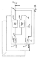
- FIG. 2A illustrates a block diagram of an example embodiment of a tuned isolation circuit.
- a transmit port at node 1 is configured to receive an outgoing signal from a communication device or other source.
- the outgoing signal is to be transmitted over a channel 210 shown as having a line impedance, Z line .
- a receive port at a node 3 is configured to receive and provide incoming signals to a communication device or other signal receiving apparatus that may connect to node 3.
- the term communication device is defined herein to mean any system or apparatus configured to communicate information or data between two locations. It is contemplated that the communication device may operate in a full-duplex mode thereby benefiting from the tuned isolation circuit as described herein.
- the channel may comprise any element or medium configured to convey information or data, such as, but not limited to, metallic conductors, twisted pair, coaxial cable, CAT5 or CAT6 cabling or any variation, such as, but not limited to, CAT5e, wireless or free space channel, waveguide, single-ended or differential transmission line, or fiber optic cable. Because the method and apparatus described herein may operate with any type channel, the channel may comprise any other channel as would be understood by one of ordinary skill in the art and the claims that follow are not limited to a particular channel.
- the embodiment shown in Figure 2A utilizes a driver amplifier 212 to connect to the transmit port at node 1.
- the driver amplifier 212 may comprise a current output driver, a voltage output driver, matched-impedance driver, or any other device capable of receiving and reproducing a transmit signal received on node 1.
- the driver amplifier 212 may be configured with or without gain, and with or without feedback.
- the output of the driver amplifier 212 connects to a first filter 220A and a second filter to 220B.
- the filters 220A, 220B may comprise any type filter configured to perform as described herein. It is contemplated that the filters 220A, 220B may comprise continuous-time filters, discrete-time filters, or a combination of both. In one embodiment, the filters 220A, 220B are configured to attenuate a signal and perform frequency specific modification or manipulation of a signal's phase. It is contemplated that the filters 220A, 220B are bi-directional thereby functioning upon a signal regardless of the direction in which a signal passes there through.
- the filters 220A, 220B are configured to have identical transfer functions, although in other embodiments it is contemplated that the filters could be configured differently. Although shown as single filters 220A, 220B, the first filter 220A may be considered as representing the transfer function between node 232 and node 2, while the second filter 220B represents the transfer function between node 232 and node 234. Thus, the response of the node itself and the signal path between the nodes is taken into consideration when arriving at the transfer function for filters 220A, 220B.
- the output of the first filter 220A connects to the node 2, which in this configuration comprises the channel.
- Node 2 also connects to an input of a differencing amplifier 224.
- the output of the second filter 220B connects to ground through a termination impedance R term and to a second input of the differencing amplifier 224.
- the termination impedance may be considered as representing any arbitrary real or reactive impedance network, implemented as discrete components or distributed elements; or synthesized using feedback methods or adaptive methods.
- the output of the differencing amplifier at node 3 connects to or comprises the receive port of a communication device.
- the outgoing signals are output from node 2 for transmission over the channel 210.
- Incoming signals are received on node 2, isolated, and provided as an output on node 3. Removal of the transmit signal from the incoming signal and isolation of the incoming signal from the transmit port occurs to achieve desired operation. Because of the operation of the embodiments shown in Figures 3-5 is generally similar, a detailed discussion of operation is provided below in conjunction with Figures 6-7 .
- the receive port derives from the output of a differencing amplifier
- numerous devices or methods may be employed to perform the differencing function with or without signal amplification, as shown more generally in Figure 2B .
- These devices and methods include, but are not limited to, one or more of active or passive circuits comprising transformers, resistive networks, and transistors. Passive differencing devices, or differencing devices without signal amplification, may reduce circuit power consumption at the expense of higher receiver noise figure.
- the claims and descriptions that follow should not be interpreted as being limited to the particular example embodiment of Figure 2A , Figure 2B , or only the elements and configurations shown.
- a differencing device 240 is shown as connecting to the Rx port and to the second filter 220B and node 2.
- the amplifier 224 of Figure 2A is but one possible differencing element and as such, the differencing device 240 may comprise any element or combination of elements.
- the differencing device may comprise only resistors, or resistors in combination with an amplifier.
- the differencing device may comprise other configurations.
- a differencing device which may also function as a summation device due to the relationship of addition and subtraction, generates a difference between two signals or adds two signals in opposite polarity to obtain a difference between the two signals.
- Figure 3 illustrates an example embodiment of a tuned isolation circuit. This is but one example embodiment and as such, the claims that follow are not limited to this particular configuration. As compared to Figure 2A , identical elements are identified with identical reference numerals and the focus of this discussion is on the aspects of Figure 3 that are different from that shown in Figure 2A .
- the output of the signal source 212 connects to a first and second delay 304A, 304B as shown.
- the delay 304 may introduce any amount of delay but the amount of delay is dependant upon the desired frequency affect on the signal passing there through.
- the delays 304 may comprise any form or type of delay comprising, but not limited to, an active delay device, a tapped delay line, a coaxial cable delay, single-ended or differential transmission lines, a lumped element delay, or a surface acoustic wave delay.
- the delay 304 may comprise a discrete element or be configured as part of the circuit or part of the printed circuit board.
- first delay 304A connects to a first attenuator 308A while the opposing side of the second delay 304B connects to a second attenuator 308B.
- the opposing terminal of the second attenuator 308A connects to node 2 while the opposing terminal of the second attenuator 308B connects to the differencing amplifier 224 and the termination impedance R term .
- the attenuators 308 may comprise any device configured to attenuate a signal passing there through. In the embodiment of Figure 3 , each attenuator provides an amount of attenuation equivalent to the square root of 1/ ⁇ , where the value ⁇ may be fixed or variable and is selected to achieve a desired receive signal transfer function for the tuned isolation circuit.
- the delays 304 and the attenuators 308 may be configured as a filter, and may comprise active elements, passive elements or a combination of both.
- the attenuators 308 may comprise reactive components, or semiconductor devices such as pin diodes, switched capacitors, or bi-directional amplifiers.
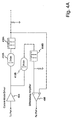
- Figure 4A illustrates an example embodiment of an example implementation of the tuned isolation circuit of Figure 3 .
- the driver amplifier comprises a current output amplifier 404 while the receive amplifier is configured as a differencing low-noise amplifier 408.
- the delays comprise similarly configured delays 412A, 412B each of which are configured to provide 1 ⁇ 2 tau ( ⁇ ) delay, where ⁇ comprises a baud period.
- the attenuators 416A, 416B comprise resistive pi type attenuators but in other embodiments the attenuators may comprise any other type of attenuator.
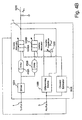
- Figure 4B illustrates a second example embodiment of an example implementation of the tuned isolation circuit of Figure 3 .
- This is but one example embodiment and as such, the claims that follow are not limited to this particular configuration.
- identical elements are identified with identical reference numerals and the focus of this discussion is on the aspects of Figure 4B that are different from those shown in Figures 3 and 4A .
- the fixed attenuators and fixed termination impedance of the example embodiment of Figure 4A are replaced by variable attenuators 1516A, 1516B and a variable termination impedance 1520.
- Variable attenuators 1516A, 1516B allow the receive signal transfer function (frequency response) of the tuned isolation circuit, as determined by attenuation factor ⁇ and discussed below in more detail in connection with Figure 9 , to be dynamically adjusted to complement the frequency response of the channel.
- variable termination impedance 1520 allows the characteristic impedance of the tuned isolation circuit, determined by R term , to be dynamically adjusted to match the characteristic impedance 1510 of the channel.
- control signals for setting the variable attenuators 1516A, 1516B and setting the variable termination impedance 1520 are derived from a channel estimator 1518 located at the receive port 3.
- the channel estimator 1518 may function as a simple signal amplitude detector, where the variable attenuator setting is based on receive signal power and the variable termination impedance setting is based on residual transmit signal power, or the channel estimator 1518 may employ more sophisticated system identification algorithms based on any system or method now available or developed in the future.
- variable attenuators 1516A, 1516B and variable termination impedance 1520 shown in Figure 4B may be employed to implement the variable attenuators 1516A, 1516B and variable termination impedance 1520 shown in Figure 4B .
- devices and methods include, but are not limited to, one or more of active or passive circuits comprising PIN diodes, field effect transistors (FETs), switched capacitors, solid-state switches, or relays.
- FETs field effect transistors
- switched capacitors solid-state switches, or relays.
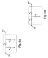
- Figure 5A illustrates an example embodiment of an attenuator.
- a first node 500 and a second node 504 provide electrical access to the attenuator.
- a resistor R 1 and R 2 connect to the first node 500.
- the opposing terminal of resistor R 1 connects to ground while the opposing terminal of resistor R 2 connects to node 504 and resistor R 3 .
- the opposing terminal of resistor R 3 connects to ground.
- the values of resistors R 1 , R 2 , R 3 are selected to achieve the desired level of attenuation.
- Figure 5B is similar to the configuration of Figure 5A , but the resistors are configured in a T-shaped configuration. As shown, resistor R 4 connects to node 500. The opposing terminal of resistor R 4 connects to resistors R 5 and R 6 . The opposing terminal of R 5 connects to ground while the opposing terminal of resistor R 6 connects to node 504. The values of resistors R 4 , R 5 , and R 6 are selected to achieve the desired level of attenuation.
- Attenuators may be configured using any device or element, including, but not limited to, resistors, capacitors, and inductors. Passive or active devices may be used. It is further contemplated that the attenuator may comprise pin diodes, switched capacitors, or variable or fixed gain bi-directional amplifiers.
- An outgoing transmit signal traverses along path 604 from node 1 to node 2, encountering isolation elements 412A and 416A before arriving at the channel 210.
- the outgoing transmit signal is not significantly altered by the isolation elements 412A and 416A, which form an all-pass (i.e. flat magnitude) network.
- the delay element 412A produces a delay of ⁇ /2 seconds and the attenuation element 416A produces an attenuation of 10 log(1/ ⁇ ) dB.
- the tuned hybrid attenuates the signal that is transmitted from the transmitter by a value that is dependant on the attenuation factor ⁇ .
- the value for ⁇ may comprise any value, it is generally desired for the attenuation factor ⁇ to be large to reduce the amount of attenuation applied to the transmit signal.
- the amount of attenuation is dependant on ⁇ and as such, the level of attenuation may be made to be less than prior art embodiments by selecting a higher value of ⁇ . If, in one embodiment, ⁇ equals 0.75, then the tuned hybrid attenuates the transmit signal by about 1.25 dB. This is an improvement over prior art hybrids, when considered in view of the other performance characteristics as defined herein.
- the relation between different ⁇ values on circuit performance is discussed below in more detail in connection with Figure 9 .
- the transmit signal encounters the delay element 412A and the attenuation element 416A, as the signal traverses from Node 1 to the positive terminal of the differencing amplifier 408.
- delay element 412A produces a delay of ⁇ /2 seconds and attenuation element 416A produces an attenuation of 10 ⁇ log(1/ ⁇ ).
- the transmit signal encounters the delay 412B and attenuator 416B, as the signal traverses from Node 1 to the negative terminal of the differencing amplifier 408.
- delay element 412B produces a delay of ⁇ /2 seconds and attenuation element 416B produces an attenuation of 10 ⁇ log(1/ ⁇ ). In other embodiments, other amounts of delay and/or attenuation may be provided.
- the delay elements 412A and 412B and the attenuation elements 416A and 416B are matched.
- the transfer functions at each input to the differencing amplifier 408 are identical as seen by a signal on path 604 and a signal on path 608.
- the transmit signal with a generally identical amount of delay and attenuation is presented to both inputs of the differencing amplifier 408.
- the differencing amplifier outputs the difference between its inputs thereby resulting in rejection of the transmit signal at node 3.
- the transfer function of H 31 represents the rejection capability of the tuned hybrid as determined by the impedance match between the termination resistor R term and channel impedance Z line ⁇ If R term and Z line are perfectly matched, the differencing amplifier results in complete rejection of the transmit signal at node 3. In other embodiments, complete rejection may not occur, but the degree of isolation between the transmit port at node 1 and the receive port at node 3 is sufficient to adequately reduce the transmit signal on the receive port at node 3 to enable accurate detection and decoding of an incoming receive signal.
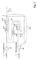
- FIG. 7 a block diagram is provided to aid in a discussion of the operation of an example implementation in response to a receive signal.
- the paths 704, 708 taken by an incoming signal are shown in Figure 7 with dashed lines.
- a signal received at the channel node 2 proceeds along paths 704 and 708.
- a signal on path 708 passes directly to the positive terminal of a low-noise differencing amplifier 408.
- the transfer function of this path is unity (1) and, as such, a signal on path 708 is not attenuated or delayed.
- a signal on path 704 encounters the attenuator 416A, the delay 412A, the output impedance of the current-mode driver 404, the delay 412B, and the attenuator 416B before arriving at the negative terminal of the differencing amplifier 408.
- the current-output driver 404 possesses a high output impedance, and therefore, does not affect the signal on path 704.
- all of the signal may be assumed as proceeding to the lower path through elements 412B, 416B, subject to the delay and attenuation of these elements 412B, 416B and then into the negative terminal of the differencing amplifier.
- the termination resistor R term terminates the incoming signal and in the embodiment shown in Figure 6 is selected to match the resistance or impedance of the channel Z line .
- the value of R term may be any real value, or a network of real and reactive impedances.
- the incoming signal should be properly terminated as it passes along path 704 if the terminating resistor R term is matched to the line.
- H - Term ⁇ 32 s ⁇ ⁇ e - s ⁇
- H 32 from node 2 to node 3 may be written as follows.
- the receive transfer function of H 32 has the effect of a high-pass channel equalization filter while the transfer function H 31 represents the rejection capability of the tuned hybrid as determined by the impedance match between the termination resistor R term and channel impedance Z line ⁇
- the receive transfer function applied to the incoming signal is thus represented by H 32 because the signal on path 708 is generally not filtered at all, while the signal on path 704 is filtered by elements 412, 416 to produce a desirable overall response. In this particular exemplary embodiment, this comprises 20 ⁇ log(1/ ⁇ ) dB of attenuation and ⁇ seconds of delay between these two paths.
- the resulting output from the differencing amplifier 408 comprises the filtered receive signal and some residual amount of transmit signal determined by the transfer function H 31 . In other embodiments, the degree of attenuation and delay may be modified depending on the amount of attenuation introduced by the attenuation element 416 and the amount of delay introduced by the delay element 412.
- the incoming signal is significantly isolated by the elements 412, 416 and, as discussed below in more detail, the frequency response of the transfer function from node 2 to node 3 modifies the incoming signal.
- the amount, type, and particulars of the modification to the incoming signal depend on the transfer function.
- a lead-lag response is generated by the attenuator and delay elements to amplify higher frequency portions of and attenuate lower frequency portions of the incoming signal, thereby resulting in high-frequency pre-emphasis.
- the amount of high-frequency pre-emphasis is directly proportional to the attenuation factor ⁇ . This is discussed below in more detail.
- the outgoing (transmit) signal applied to node 1 is not significantly altered by the isolation elements 412A and 416A.
- the delay element 412A and the attenuation element 416A form an all-pass (i.e. flat magnitude) network.
- the attenuation of the all-pass network is half the attenuation applied to the incoming signal along path 704, or 10 ⁇ log(1/ ⁇ ). Therefore, the attenuation applied to the transmit signal is inversely proportional to the attenuation factor ⁇ .
- the attenuation factor ⁇ can be adjusted to produce an optimal balance between high-frequency pre-emphasis of the incoming (receive) signal and attenuation of the outgoing (transmit) signal.
- a large attenuation factor ⁇ can be used to effect significant high-frequency pre-emphasis of the receive signal with little attenuation of the transmit signal.
- a third advantage to this embodiment and the resulting method of operation is the input return loss seen at node 2 is high such that receive signals incident on node 2 are transferred to the isolation circuit with minimal loss.
- the termination network R term may be selected to match the impedance Z line presented by the channel to produce maximum isolation between transmit and receive signals. Since the current output driver 404 has high output impedance, the impedance seen at node 2 is determined by the termination network R term . Thus, the matching of R term and Z line to maximize transmit/receive isolation ensures high input return loss at node 2 and maximum power transfer of incoming signals to the isolation circuit.
- the current output driver 404 or other signal source may be configured with a high output impedance to thereby ensure high input return loss.
- a signal source other than a current output driver 404 may be used, which may or may not have a high output impedance, because the transfer functions associated with the isolation circuit (H 21 , H 31 , and H 32 ) are independent of the output impedance of the driver.
- V ⁇ V 2 s ⁇ ⁇ ⁇ e - s ⁇ ⁇ R out ⁇ R term / R out + R term - Z line
- R out ⁇ R term / R out + R term + Z line V 2 s ⁇ ⁇ ⁇ e - s ⁇ ⁇ ⁇ L
- V + V 2 s ⁇ 1 + ⁇ ⁇ e - s ⁇ ⁇ ⁇ L
- V - V 2 s ⁇ 1 + ⁇ L ⁇ ⁇ ⁇ e - s ⁇
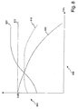
- Figure 8 illustrates an exemplary signal plot of an exemplary receive signal frequency response of a tuned hybrid. This should be considered an exemplary plot and is provided for purposes of discussion. Depending on the elements within the tuned hybrid, the receive signal frequency response of the tuned hybrid will vary. Thus, by varying the amount of the delay and attenuation it is contemplated that different frequency responses may be obtained. It is further contemplated that variable delay elements and variable attenuator elements may be employed to effect dynamic control of the tuned hybrid frequency response. As shown, a vertical axis 804 represents power or magnitude and is shown in dB scale. The horizontal axis 808 represents frequency. A zero dB plot 812 represents the zero dB axis across all frequencies and is provided for reference.
- the generally accepted low-pass frequency response of the channel is shown by plot 820.
- the channel attenuates all frequencies, with higher frequencies being attenuated to a greater degree.
- the high degree of attenuation of higher frequencies represents a drawback with high frequency communication and is a design challenge that must be overcome to receive and decode a communication signal.
- Plot 822 represents the receive signal frequency response of one example embodiment of a tuned hybrid.
- the receive signal frequency response of the tuned hybrid is configured as a lead-lag type filter response.
- the tuned hybrid attenuates a received signal, while mid-frequencies experience little attenuation.
- the tuned hybrid is configured with gain at high frequencies. Thus, portions of the receive signal in the high frequency spectrum are slightly amplified. On low-pass channels, this high-frequency pre-emphasis is highly desirable.
- the resulting signal plot 816 represents the combined transfer function of the channel and the tuned hybrid. As can be seen, plot 816 has the benefit of being generally flat across a larger portion of the frequency spectrum of the receive signal.
- the tuned hybrid circuit provides the advantage of not only providing isolation and rejection, but also equalizing the channel. As a result, less, or possibly no, equalization may be required within the receiver, or the degree and complexity of downstream equalization may be reduced. This is an advantage over prior art hybrids that traditionally have an all-pass frequency response with respect to the receive signal.
- Figure 9 illustrates exemplary signal plots generated in response to varying the value of the attenuation factor ⁇ in an exemplary tuned hybrid. This should be considered an exemplary plot and is provided for purposes of discussion. By varying the amount of the delay, attenuation, or both, it is contemplated that a different receive signal frequency response may be obtained. As shown, a vertical axis 904 represents signal power or magnitude and is shown in dB scale. The horizontal axis 908 represents frequency.
- a zero dB plot 812 represents the zero dB axis across all frequencies and is provided for reference. The generally accepted frequency response of the channel is shown by plot 820. These plots are discussed above in connection with Figure 8 and hence are not discussed again.
- Plots 912, 916, and 920 represent the receive signal frequency response of the tuned hybrid for different values of attenuation factor ⁇ .
- plot 920 represents an ⁇ value that is larger than the ⁇ value associated a tuned hybrid having a frequency response of the other two plots 912, 916.
- a large ⁇ value may be selected for a severely low-pass channel, such as a long length of twisted-pair wire cable, because a larger ⁇ value provides the advantage of increasing the gain for higher frequencies signal portions, which are greatly attenuated by long lines, while reducing the amount of signal attenuation in the transmit path of the tuned hybrid circuit.
- plot 912 is associated with a small attenuation factor ⁇ value.
- the amount of attenuation at low frequencies is lower than compared to plot 920.
- lower values of ⁇ which yield a frequency response for the tuned hybrid as shown by plot 912, are well suited for less severe low-pass channels, such as a short length of twisted-pair wire cable.
- the attenuation of the signal, at all frequencies occurs to a lesser extent than would be experienced on a long length of twisted-pair wire cable.
- the smaller ⁇ value is well suited in this case because a signal arriving over a less severe low-pass channel does not require as much amplification of the higher frequency components.
- Plot 916 illustrates a plot of the frequency response of a tuned hybrid having a value of ⁇ that is between the value of ⁇ that generated plot 920 and the value of ⁇ that generated plot 912. It is contemplated that intermediate values for ⁇ may be selected to suit a wide range of channel low-pass characteristics. Although exemplary channel low-pass characteristics to ⁇ value pairs are provided, it is contemplated that any ⁇ value may be selected for a given channel low-pass characteristic, depending on the desired design and operational parameters of the tuned hybrid.
- the value of ⁇ may be permanently set, or adaptable to an ideal value based on the characteristics of the channel.
- the receiver may detect the power level or magnitude of a received signal using at channel estimator at the receive port. Based on the power level of the receive signal, the low-pass nature of the channel may be extrapolated, and a value of ⁇ selected that is optimized for the channel. In particular, the level of high frequency gain, low frequency attenuation, or both, may be tailored to best suit the detected characteristics of the channel. This operation may occur periodically, as part of an initialization process, or both. In other embodiments, the value of ⁇ may be manually set.
- Figure 10A illustrates a block diagram of an example embodiment of a tuned hybrid in a differential mode configuration. It is contemplated that other configurations for a differential mode tuned hybrid exist and hence, this example embodiment is provided for purposes of discussion.
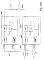
- Figure 10B illustrates an example embodiment of Figure 10A where the differencing amplifier is replaced more generally by a differencing device. As is generally understood, the amplifier of Figure 10A may be configured as a differencing device and thus the amplifier is one example of a differencing device.
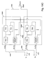
- Figure 10C illustrates an example embodiment where the differencing amplifier is replaced by a summing device.
- the summing device may comprise any element, such as in one example embodiment it may comprise a network of resistors.
- the differencing and summing devices shown in Figures 10B and 10C respectively, may be implemented as active or passive circuits that may or may not employ signal amplification.
- the differencing and summing devices may be implemented as amplifiers or any other element.
- the differencing device may comprise resistors.
- summing devices can be simpler to implement than differencing devices. As such, the claims that follow should not be interpreted as being limited to the particular example embodiments illustrated in Figures 10A-10C .
- the channel comprises a twisted pair channel comprising conductors 1004A, 1004B.
- Numerous tuned hybrids in differential mode configuration may be utilized, such as in a CAT5 Ethernet environment.
- the conductor 1004A connects to a first tuned hybrid 1008A while the second conductor 1004B connects to a second tuned hybrid 1008B.
- other channels may be utilized.
- a multi-channel communication system may utilize one or more tuned hybrids as described herein.
- the first tuned hybrid 1008A and the second tuned hybrid 1008B operate as described above and hence, an explanation of the operation of these devices is not provided again.
- the first tuned hybrid further comprises a transmit port 1020 and a receive port 1024.
- the second tuned hybrid comprises a transmit port 1039 and a receive port 1034.
- the transmit ports 1020, 1039 serve as and/or connect to the two conductor transmit ports associated with a communication device (not shown).
- the receive ports 1024, 1034 serve as or connect to the two conductor receiver ports that are associated with a communication device (not shown).
- more than one two conductor channel may be utilized.
- some communication systems, such as communication systems that utilize CAT5 cabling utilize more than one channel.
- the tuned hybrid described herein may be utilized in such an embodiment.
- a channel with greater than or less than two conductors may be utilized.
- the configuration comprises a differencing device or summing device
- the output of the receiver channels 1324, 1334 may optionally feed into an amplifier.
Landscapes
- Engineering & Computer Science (AREA)
- Computer Networks & Wireless Communication (AREA)
- Signal Processing (AREA)
- Amplifiers (AREA)
- Cable Transmission Systems, Equalization Of Radio And Reduction Of Echo (AREA)
- Transmitters (AREA)
- Networks Using Active Elements (AREA)
Claims (19)
- Procédé de génération d'un signal reçu isolé provenant d'un canal (210) qui transporte également un signal transmis, le procédé comprenant :la réception d'un signal entrant provenant du canal ;la réception d'un signal sortant, le signal sortant devant être envoyé via le canal ;le filtrage du signal sortant par un premier filtre bidirectionnel (220A) pour créer un premier signal sortant filtré ;le filtrage du signal sortant par un deuxième filtre bidirectionnel (220B) pour créer un deuxième signal sortant filtré, le premier filtre bidirectionnel et le deuxième filtre bidirectionnel ayant des fonctions de transfert identiques ;la génération d'une différence entre le premier signal sortant filtré et le deuxième signal sortant filtré ;le filtrage du signal entrant par le premier filtre bidirectionnel et le deuxième filtre bidirectionnel pour créer un signal entrant filtré ;la génération d'un signal de différence entre le signal entrant filtré et le signal entrant ; etla sortie dudit signal de différence, dans lequel le premier signal sortant filtré et le deuxième signal sortant filtré sont annulés avant de sortir ledit signal de différence, ledit signal de différence étant le signal reçu isolé.
- Procédé selon la revendication 1, comprenant en outre l'isolation du signal reçu en mode différentiel.
- Procédé selon la revendication 1, dans lequel la génération d'une différence comprend la mise en oeuvre d'une somme de signaux.
- Procédé selon la revendication 1, dans lequel le filtrage comprend un retardement et une atténuation.
- Procédé selon la revendication 1, dans lequel le filtrage comprend un filtrage de réponse passe-tout.
- Procédé selon la revendication 1, dans lequel le filtrage comprend la génération d'une réponse en fréquence qui égalise partiellement ou complètement les effets dispersifs du canal.
- Procédé selon la revendication 1, dans lequel le filtrage comprend la génération dynamique, via un processus d'adaptation, d'une réponse en fréquence qui dépend des caractéristiques du canal.
- Procédé selon la revendication 1, comprenant en outre la mise en correspondance d'une impédance du canal.
- Procédé selon la revendication 1, comprenant en outre la mise en correspondance dynamique d'une impédance du canal.
- Unité d'isolation de signal, comprenant :un port de canal (2) configuré pour se connecter à un canal (210) ;un port de transmission (1) configuré pour se connecter à un transmetteur ;un port de réception (13) configuré pour se connecter à un récepteur ;un pilote en mode courant comprenant une entrée connectée au port de transmission et une sortie connectée à un premier filtre et à un deuxième filtre ;le premier filtre étant connecté à la sortie du pilote en mode courant et au port de canal ;le deuxième filtre étant connecté à la sortie du pilote en mode courant et à un dispositif de différentiation (240) ;le dispositif de différentiation comprenant :une sortie connectée au port récepteur ;une première entrée connectée au port de canal ;une deuxième entrée connectée au deuxième filtre ;dans laquelle le premier filtre se connecte au port de canal, et le premier filtre et le deuxième filtre sont bidirectionnels et ont des fonctions de transfert généralement similaires.
- Unité selon la revendication 10, dans laquelle la fonction de transfert de l'unité d'isolation de signal est dépendante de la fréquence.
- Unité selon la revendication 10, dans laquelle la fonction de transfert de l'unité d'isolation de signal est autre qu'un filtre passe-tout.
- Unité selon la revendication 10, dans laquelle la fonction de transfert de l'unité d'isolation de signal est dynamiquement ajustable en fonction des caractéristiques du canal.
- Unité selon la revendication 10, comprenant en outre une impédance de terminaison (Rterm) connectée au port de canal, configurée pour correspondre à l'impédance du canal.
- Unité selon la revendication 11, dans laquelle l'impédance de terminaison est dynamiquement ajustable pour correspondre à l'impédance du canal.
- Unité selon la revendication 10, dans laquelle l'unité d'isolation de signal est configurée en mode différentiel.
- Unité selon la revendication 11, dans laquelle le dispositif de différentiation est plutôt configuré pour effectuer une somme de signaux.
- Unité selon la revendication 10, dans laquelle le premier filtre et le deuxième filtre comprennent chacun un retardateur et un atténuateur.
- Unité selon la revendication 18, dans laquelle l'atténuateur comprend une ou plusieurs résistances.
Applications Claiming Priority (3)
| Application Number | Priority Date | Filing Date | Title |
|---|---|---|---|
| US11/002,953 US7460662B2 (en) | 2004-12-02 | 2004-12-02 | Isolation of transmit and receive signals in full-duplex communication systems |
| US11/242,970 US7738654B2 (en) | 2004-12-02 | 2005-10-04 | Isolation of transmit and receive signals |
| PCT/US2005/043232 WO2006060441A2 (fr) | 2004-12-02 | 2005-11-29 | Isolation de signaux d'emission et de reception |
Publications (3)
| Publication Number | Publication Date |
|---|---|
| EP1829351A2 EP1829351A2 (fr) | 2007-09-05 |
| EP1829351A4 EP1829351A4 (fr) | 2010-07-14 |
| EP1829351B1 true EP1829351B1 (fr) | 2015-10-21 |
Family
ID=36565665
Family Applications (1)
| Application Number | Title | Priority Date | Filing Date |
|---|---|---|---|
| EP05852480.2A Expired - Lifetime EP1829351B1 (fr) | 2004-12-02 | 2005-11-29 | Isolation de signaux d'emission et de reception |
Country Status (5)
| Country | Link |
|---|---|
| US (1) | US7738654B2 (fr) |
| EP (1) | EP1829351B1 (fr) |
| JP (1) | JP4866979B2 (fr) |
| TW (1) | TWI341679B (fr) |
| WO (1) | WO2006060441A2 (fr) |
Families Citing this family (21)
| Publication number | Priority date | Publication date | Assignee | Title |
|---|---|---|---|---|
| ES2330178B1 (es) * | 2007-06-25 | 2010-08-30 | Diseño De Sistemas En Silicio, S.A. | Repetidor de señal de un solo puerto. |
| US7804859B2 (en) * | 2008-06-30 | 2010-09-28 | Silicon Laboratories, Inc. | System and method of providing electrical isolation |
| US8095710B2 (en) * | 2008-06-30 | 2012-01-10 | Silicon Laboratories Inc. | System and method of providing electrical isolation |
| US8718586B2 (en) * | 2009-06-30 | 2014-05-06 | Anritsu Company | Apparatus for enhancing the dynamic range of shockline-based sampling receivers |
| EP2467948B1 (fr) * | 2009-08-19 | 2016-08-17 | Ikanos Communications, Inc. | Hybride intégré adaptatif avec adaptation complexe destiné à des systèmes de lignes d'abonnés numériques |
| WO2013095536A1 (fr) | 2011-12-22 | 2013-06-27 | Intel Corporation | Architecture d'entrée/sortie sur boîtier |
| EP2672631B1 (fr) | 2012-06-07 | 2014-12-24 | Telefonaktiebolaget L M Ericsson (publ) | Émetteur-récepteur sans duplexeur et appareil de communication |
| EP2733855B1 (fr) | 2012-11-15 | 2016-07-27 | Telefonaktiebolaget LM Ericsson (publ) | Module frontal émetteur-récepteur |
| BR112015022333B1 (pt) | 2013-03-14 | 2022-08-23 | Telefonaktiebolaget L M Ericsson (Publ) | Transceptor, e, dispositivo de comunicação |
| WO2014173459A1 (fr) | 2013-04-26 | 2014-10-30 | Telefonaktiebolaget L M Ericsson (Publ) | Agencement d'émetteur-récepteur, dispositif de communication, procédé et programme informatique |
| MY185907A (en) | 2013-04-30 | 2021-06-14 | Ericsson Telefon Ab L M | Transceiver arrangement, communication device, method and computer program |
| US20150044981A1 (en) * | 2013-08-12 | 2015-02-12 | Yao H. Kuo | Multi-Notch Filter and Method for Multi-Notch Filtering |
| EP3097645B1 (fr) | 2014-01-21 | 2017-08-23 | Telefonaktiebolaget LM Ericsson (publ) | Montage émetteur-récepteur et dispositif de communication |
| WO2016066278A1 (fr) | 2014-10-29 | 2016-05-06 | Telefonaktiebolaget L M Ericsson (Publ) | Configuration d'émetteur-récepteur et dispositif de communication |
| US9966931B2 (en) * | 2014-11-27 | 2018-05-08 | Infineon Technologies Ag | Active quasi circulator |
| US10361786B1 (en) * | 2015-10-06 | 2019-07-23 | Radin Global | Phase optimization technique in high-speed simultaneous bi-directional links |
| US10365329B2 (en) * | 2016-05-26 | 2019-07-30 | Infineon Technologies Ag | Measurements in switch devices |
| US11323181B2 (en) * | 2016-10-05 | 2022-05-03 | Radin Global | Phase optimization technique in high-speed simultaneous bidirectional links |
| US10904042B2 (en) | 2017-09-29 | 2021-01-26 | Tektronix, Inc. | Passive variable continuous time linear equalizer with attenuation and frequency control |
| JP7558642B2 (ja) * | 2018-02-05 | 2024-10-01 | テクトロニクス・インコーポレイテッド | ノイズ・フィルタ及びノイズ低減方法 |
| CN118868999B (zh) * | 2024-09-26 | 2025-10-21 | 成都新欣神风电子科技有限公司 | 收发共用高功率微波防护电路及防护方法 |
Family Cites Families (10)
| Publication number | Priority date | Publication date | Assignee | Title |
|---|---|---|---|---|
| JPS55133121A (en) * | 1979-04-04 | 1980-10-16 | Hitachi Ltd | Conversion circuit of two to four lines |
| JPH0787404B2 (ja) * | 1987-12-16 | 1995-09-20 | 株式会社ミュ−コム | テレビ電話機に使用する伝送装置 |
| US5333194A (en) * | 1990-10-15 | 1994-07-26 | Glenayre Electronics, Inc. | Autoequalizing bidirectional-to-unidirectional hybrid network |
| US5657384A (en) * | 1995-03-10 | 1997-08-12 | Tandy Corporation | Full duplex speakerphone |
| US6373908B2 (en) * | 1998-11-11 | 2002-04-16 | Broadcom Corporation | Adaptive electronic transmission signal cancellation apparatus for full duplex communication |
| FR2798022B1 (fr) * | 1999-08-30 | 2008-09-26 | St Microelectronics Sa | Circuit hybride d'emission-reception |
| US7050574B1 (en) * | 1999-09-30 | 2006-05-23 | Stmicroelectronics, Inc. | Telephone line interface circuit and method |
| US6836544B1 (en) * | 2000-08-24 | 2004-12-28 | Intel Corporation | Sidestone reduction in full duplex transceivers |
| WO2002065662A2 (fr) * | 2001-02-01 | 2002-08-22 | Analog Devices, Inc. | Interface de ligne comportant une impedance a l'adaptation couplee avec une retroaction de gain |
| US7020277B1 (en) * | 2001-12-05 | 2006-03-28 | Lsi Logic Corporation | DSL line interface having low-pass filter characteristic with reduced external components |
-
2005
- 2005-10-04 US US11/242,970 patent/US7738654B2/en not_active Expired - Lifetime
- 2005-11-29 WO PCT/US2005/043232 patent/WO2006060441A2/fr not_active Ceased
- 2005-11-29 JP JP2007544450A patent/JP4866979B2/ja not_active Expired - Fee Related
- 2005-11-29 EP EP05852480.2A patent/EP1829351B1/fr not_active Expired - Lifetime
- 2005-12-01 TW TW094142253A patent/TWI341679B/zh not_active IP Right Cessation
Also Published As
| Publication number | Publication date |
|---|---|
| WO2006060441A2 (fr) | 2006-06-08 |
| JP4866979B2 (ja) | 2012-02-01 |
| US7738654B2 (en) | 2010-06-15 |
| WO2006060441A3 (fr) | 2007-11-15 |
| JP2008522553A (ja) | 2008-06-26 |
| EP1829351A4 (fr) | 2010-07-14 |
| TW200637347A (en) | 2006-10-16 |
| TWI341679B (en) | 2011-05-01 |
| US20060133599A1 (en) | 2006-06-22 |
| EP1829351A2 (fr) | 2007-09-05 |
Similar Documents
| Publication | Publication Date | Title |
|---|---|---|
| US7738654B2 (en) | Isolation of transmit and receive signals | |
| US7460662B2 (en) | Isolation of transmit and receive signals in full-duplex communication systems | |
| US7164764B2 (en) | Method and apparatus for precode crosstalk mitigation | |
| US5952914A (en) | Power line communication systems | |
| US8787488B2 (en) | System, method and apparatus for crosstalk cancellation | |
| US9118469B2 (en) | Reducing electromagnetic interference in a received signal | |
| US6912208B2 (en) | Method and apparatus for equalization and crosstalk mitigation | |
| CN108702172B (zh) | 自干扰抑制结构的系统和方法 | |
| US10505571B1 (en) | Estimation of interference suppression filters using selective signal switching | |
| JPH04233313A (ja) | トランスバーサル等化器と入力電気信号等化方法と光波通信システム | |
| EP2503704B1 (fr) | Procédé et dispositif d'égalisation et d'atténuation de la diaphonie | |
| US8126078B2 (en) | Method and apparatus for reducing noise in an unbalanced channel using common mode component | |
| EP1443676A2 (fr) | Dispositif et méthode de réduction de la diaphonie | |
| US5335363A (en) | Signal interference reduction device and method | |
| EP1420556A2 (fr) | Banc de filtres pour liaisons d'ethernet longues | |
| EP0375015B1 (fr) | Procédé et dispositif d'annulation adaptative numérique de l'écho généré dans des liaisons téléphoniques à caractéristiques variables dans le temps | |
| US7366231B2 (en) | Sub-block domain transformation multiple signal processing | |
| US5506549A (en) | Cable equalizer | |
| EP4012934A1 (fr) | Dispositif et procédé de traitement de signal de bruit | |
| EP1675288B1 (fr) | Dispositif pour transmettre un signal de donnees dans un reseau de television par cable | |
| JP2002185261A (ja) | 増幅装置 | |
| EP2343833B1 (fr) | Méthode et système pour équilibrer l'impédance dans un circuit hybride | |
| US20040177379A1 (en) | Method and apparatus for isolating signals in RF circuits and systems |
Legal Events
| Date | Code | Title | Description |
|---|---|---|---|
| PUAI | Public reference made under article 153(3) epc to a published international application that has entered the european phase |
Free format text: ORIGINAL CODE: 0009012 |
|
| 17P | Request for examination filed |
Effective date: 20070628 |
|
| AK | Designated contracting states |
Kind code of ref document: A2 Designated state(s): AT BE BG CH CY CZ DE DK EE ES FI FR GB GR HU IE IS IT LI LT LU LV MC NL PL PT RO SE SI SK TR |
|
| AX | Request for extension of the european patent |
Extension state: AL BA HR MK YU |
|
| R17D | Deferred search report published (corrected) |
Effective date: 20071115 |
|
| RIC1 | Information provided on ipc code assigned before grant |
Ipc: H04M 9/00 20060101ALI20071203BHEP Ipc: H04M 9/08 20060101AFI20071203BHEP |
|
| DAX | Request for extension of the european patent (deleted) | ||
| A4 | Supplementary search report drawn up and despatched |
Effective date: 20100611 |
|
| RIC1 | Information provided on ipc code assigned before grant |
Ipc: H04B 1/58 20060101ALI20100607BHEP Ipc: H04M 9/00 20060101ALI20100607BHEP Ipc: H04M 9/08 20060101AFI20071203BHEP |
|
| 17Q | First examination report despatched |
Effective date: 20111121 |
|
| RAP1 | Party data changed (applicant data changed or rights of an application transferred) |
Owner name: MARVELL INTERNATIONAL LTD. |
|
| RAP1 | Party data changed (applicant data changed or rights of an application transferred) |
Owner name: MARVELL INTERNATIONAL, LTD. |
|
| GRAP | Despatch of communication of intention to grant a patent |
Free format text: ORIGINAL CODE: EPIDOSNIGR1 |
|
| INTG | Intention to grant announced |
Effective date: 20150714 |
|
| GRAS | Grant fee paid |
Free format text: ORIGINAL CODE: EPIDOSNIGR3 |
|
| GRAA | (expected) grant |
Free format text: ORIGINAL CODE: 0009210 |
|
| AK | Designated contracting states |
Kind code of ref document: B1 Designated state(s): AT BE BG CH CY CZ DE DK EE ES FI FR GB GR HU IE IS IT LI LT LU LV MC NL PL PT RO SE SI SK TR |
|
| REG | Reference to a national code |
Ref country code: GB Ref legal event code: FG4D Ref country code: NL Ref legal event code: MP Effective date: 20151021 |
|
| REG | Reference to a national code |
Ref country code: CH Ref legal event code: EP |
|
| REG | Reference to a national code |
Ref country code: AT Ref legal event code: REF Ref document number: 757290 Country of ref document: AT Kind code of ref document: T Effective date: 20151115 |
|
| REG | Reference to a national code |
Ref country code: FR Ref legal event code: PLFP Year of fee payment: 11 |
|
| REG | Reference to a national code |
Ref country code: IE Ref legal event code: FG4D |
|
| REG | Reference to a national code |
Ref country code: DE Ref legal event code: R096 Ref document number: 602005047763 Country of ref document: DE |
|
| REG | Reference to a national code |
Ref country code: LT Ref legal event code: MG4D |
|
| REG | Reference to a national code |
Ref country code: AT Ref legal event code: MK05 Ref document number: 757290 Country of ref document: AT Kind code of ref document: T Effective date: 20151021 |
|
| PG25 | Lapsed in a contracting state [announced via postgrant information from national office to epo] |
Ref country code: NL Free format text: LAPSE BECAUSE OF FAILURE TO SUBMIT A TRANSLATION OF THE DESCRIPTION OR TO PAY THE FEE WITHIN THE PRESCRIBED TIME-LIMIT Effective date: 20151021 Ref country code: IT Free format text: LAPSE BECAUSE OF FAILURE TO SUBMIT A TRANSLATION OF THE DESCRIPTION OR TO PAY THE FEE WITHIN THE PRESCRIBED TIME-LIMIT Effective date: 20151021 Ref country code: ES Free format text: LAPSE BECAUSE OF FAILURE TO SUBMIT A TRANSLATION OF THE DESCRIPTION OR TO PAY THE FEE WITHIN THE PRESCRIBED TIME-LIMIT Effective date: 20151021 Ref country code: IS Free format text: LAPSE BECAUSE OF FAILURE TO SUBMIT A TRANSLATION OF THE DESCRIPTION OR TO PAY THE FEE WITHIN THE PRESCRIBED TIME-LIMIT Effective date: 20160221 Ref country code: LT Free format text: LAPSE BECAUSE OF FAILURE TO SUBMIT A TRANSLATION OF THE DESCRIPTION OR TO PAY THE FEE WITHIN THE PRESCRIBED TIME-LIMIT Effective date: 20151021 |
|
| PG25 | Lapsed in a contracting state [announced via postgrant information from national office to epo] |
Ref country code: PT Free format text: LAPSE BECAUSE OF FAILURE TO SUBMIT A TRANSLATION OF THE DESCRIPTION OR TO PAY THE FEE WITHIN THE PRESCRIBED TIME-LIMIT Effective date: 20160222 Ref country code: AT Free format text: LAPSE BECAUSE OF FAILURE TO SUBMIT A TRANSLATION OF THE DESCRIPTION OR TO PAY THE FEE WITHIN THE PRESCRIBED TIME-LIMIT Effective date: 20151021 Ref country code: PL Free format text: LAPSE BECAUSE OF FAILURE TO SUBMIT A TRANSLATION OF THE DESCRIPTION OR TO PAY THE FEE WITHIN THE PRESCRIBED TIME-LIMIT Effective date: 20151021 Ref country code: FI Free format text: LAPSE BECAUSE OF FAILURE TO SUBMIT A TRANSLATION OF THE DESCRIPTION OR TO PAY THE FEE WITHIN THE PRESCRIBED TIME-LIMIT Effective date: 20151021 Ref country code: SE Free format text: LAPSE BECAUSE OF FAILURE TO SUBMIT A TRANSLATION OF THE DESCRIPTION OR TO PAY THE FEE WITHIN THE PRESCRIBED TIME-LIMIT Effective date: 20151021 Ref country code: GR Free format text: LAPSE BECAUSE OF FAILURE TO SUBMIT A TRANSLATION OF THE DESCRIPTION OR TO PAY THE FEE WITHIN THE PRESCRIBED TIME-LIMIT Effective date: 20160122 Ref country code: LV Free format text: LAPSE BECAUSE OF FAILURE TO SUBMIT A TRANSLATION OF THE DESCRIPTION OR TO PAY THE FEE WITHIN THE PRESCRIBED TIME-LIMIT Effective date: 20151021 |
|
| REG | Reference to a national code |
Ref country code: CH Ref legal event code: PL |
|
| REG | Reference to a national code |
Ref country code: DE Ref legal event code: R097 Ref document number: 602005047763 Country of ref document: DE |
|
| PG25 | Lapsed in a contracting state [announced via postgrant information from national office to epo] |
Ref country code: LI Free format text: LAPSE BECAUSE OF NON-PAYMENT OF DUE FEES Effective date: 20151130 Ref country code: MC Free format text: LAPSE BECAUSE OF FAILURE TO SUBMIT A TRANSLATION OF THE DESCRIPTION OR TO PAY THE FEE WITHIN THE PRESCRIBED TIME-LIMIT Effective date: 20151021 Ref country code: CZ Free format text: LAPSE BECAUSE OF FAILURE TO SUBMIT A TRANSLATION OF THE DESCRIPTION OR TO PAY THE FEE WITHIN THE PRESCRIBED TIME-LIMIT Effective date: 20151021 Ref country code: CH Free format text: LAPSE BECAUSE OF NON-PAYMENT OF DUE FEES Effective date: 20151130 |
|
| REG | Reference to a national code |
Ref country code: IE Ref legal event code: MM4A |
|
| PLBE | No opposition filed within time limit |
Free format text: ORIGINAL CODE: 0009261 |
|
| STAA | Information on the status of an ep patent application or granted ep patent |
Free format text: STATUS: NO OPPOSITION FILED WITHIN TIME LIMIT |
|
| PG25 | Lapsed in a contracting state [announced via postgrant information from national office to epo] |
Ref country code: DK Free format text: LAPSE BECAUSE OF FAILURE TO SUBMIT A TRANSLATION OF THE DESCRIPTION OR TO PAY THE FEE WITHIN THE PRESCRIBED TIME-LIMIT Effective date: 20151021 Ref country code: EE Free format text: LAPSE BECAUSE OF FAILURE TO SUBMIT A TRANSLATION OF THE DESCRIPTION OR TO PAY THE FEE WITHIN THE PRESCRIBED TIME-LIMIT Effective date: 20151021 Ref country code: SK Free format text: LAPSE BECAUSE OF FAILURE TO SUBMIT A TRANSLATION OF THE DESCRIPTION OR TO PAY THE FEE WITHIN THE PRESCRIBED TIME-LIMIT Effective date: 20151021 Ref country code: RO Free format text: LAPSE BECAUSE OF FAILURE TO SUBMIT A TRANSLATION OF THE DESCRIPTION OR TO PAY THE FEE WITHIN THE PRESCRIBED TIME-LIMIT Effective date: 20151021 |
|
| 26N | No opposition filed |
Effective date: 20160722 |
|
| PG25 | Lapsed in a contracting state [announced via postgrant information from national office to epo] |
Ref country code: IE Free format text: LAPSE BECAUSE OF NON-PAYMENT OF DUE FEES Effective date: 20151129 |
|
| REG | Reference to a national code |
Ref country code: FR Ref legal event code: PLFP Year of fee payment: 12 |
|
| PG25 | Lapsed in a contracting state [announced via postgrant information from national office to epo] |
Ref country code: SI Free format text: LAPSE BECAUSE OF FAILURE TO SUBMIT A TRANSLATION OF THE DESCRIPTION OR TO PAY THE FEE WITHIN THE PRESCRIBED TIME-LIMIT Effective date: 20151021 |
|
| PG25 | Lapsed in a contracting state [announced via postgrant information from national office to epo] |
Ref country code: BE Free format text: LAPSE BECAUSE OF FAILURE TO SUBMIT A TRANSLATION OF THE DESCRIPTION OR TO PAY THE FEE WITHIN THE PRESCRIBED TIME-LIMIT Effective date: 20151021 |
|
| PG25 | Lapsed in a contracting state [announced via postgrant information from national office to epo] |
Ref country code: BG Free format text: LAPSE BECAUSE OF FAILURE TO SUBMIT A TRANSLATION OF THE DESCRIPTION OR TO PAY THE FEE WITHIN THE PRESCRIBED TIME-LIMIT Effective date: 20151021 Ref country code: HU Free format text: LAPSE BECAUSE OF FAILURE TO SUBMIT A TRANSLATION OF THE DESCRIPTION OR TO PAY THE FEE WITHIN THE PRESCRIBED TIME-LIMIT; INVALID AB INITIO Effective date: 20051129 |
|
| PG25 | Lapsed in a contracting state [announced via postgrant information from national office to epo] |
Ref country code: CY Free format text: LAPSE BECAUSE OF FAILURE TO SUBMIT A TRANSLATION OF THE DESCRIPTION OR TO PAY THE FEE WITHIN THE PRESCRIBED TIME-LIMIT Effective date: 20151021 |
|
| PG25 | Lapsed in a contracting state [announced via postgrant information from national office to epo] |
Ref country code: TR Free format text: LAPSE BECAUSE OF FAILURE TO SUBMIT A TRANSLATION OF THE DESCRIPTION OR TO PAY THE FEE WITHIN THE PRESCRIBED TIME-LIMIT Effective date: 20151021 |
|
| REG | Reference to a national code |
Ref country code: FR Ref legal event code: PLFP Year of fee payment: 13 |
|
| PG25 | Lapsed in a contracting state [announced via postgrant information from national office to epo] |
Ref country code: LU Free format text: LAPSE BECAUSE OF NON-PAYMENT OF DUE FEES Effective date: 20151129 |
|
| REG | Reference to a national code |
Ref country code: DE Ref legal event code: R081 Ref document number: 602005047763 Country of ref document: DE Owner name: MARVELL ASIA PTE, LTD., SG Free format text: FORMER OWNER: MARVELL INTERNATIONAL LTD., HAMILTON, BM Ref country code: DE Ref legal event code: R082 Ref document number: 602005047763 Country of ref document: DE Representative=s name: GRUENECKER PATENT- UND RECHTSANWAELTE PARTG MB, DE |
|
| REG | Reference to a national code |
Ref country code: GB Ref legal event code: 732E Free format text: REGISTERED BETWEEN 20201022 AND 20201028 |
|
| P01 | Opt-out of the competence of the unified patent court (upc) registered |
Effective date: 20230508 |
|
| PGFP | Annual fee paid to national office [announced via postgrant information from national office to epo] |
Ref country code: DE Payment date: 20241128 Year of fee payment: 20 |
|
| PGFP | Annual fee paid to national office [announced via postgrant information from national office to epo] |
Ref country code: GB Payment date: 20241126 Year of fee payment: 20 |
|
| PGFP | Annual fee paid to national office [announced via postgrant information from national office to epo] |
Ref country code: FR Payment date: 20241126 Year of fee payment: 20 |
|
| REG | Reference to a national code |
Ref country code: DE Ref legal event code: R071 Ref document number: 602005047763 Country of ref document: DE |
|
| REG | Reference to a national code |
Ref country code: GB Ref legal event code: PE20 Expiry date: 20251128 |