EP3097645B1 - Montage émetteur-récepteur et dispositif de communication - Google Patents
Montage émetteur-récepteur et dispositif de communication Download PDFInfo
- Publication number
- EP3097645B1 EP3097645B1 EP14701074.8A EP14701074A EP3097645B1 EP 3097645 B1 EP3097645 B1 EP 3097645B1 EP 14701074 A EP14701074 A EP 14701074A EP 3097645 B1 EP3097645 B1 EP 3097645B1
- Authority
- EP
- European Patent Office
- Prior art keywords
- filters
- type
- arrangement
- frequency
- transmitter
- Prior art date
- Legal status (The legal status is an assumption and is not a legal conclusion. Google has not performed a legal analysis and makes no representation as to the accuracy of the status listed.)
- Active
Links
Images

Classifications
-
- H—ELECTRICITY
- H04—ELECTRIC COMMUNICATION TECHNIQUE
- H04B—TRANSMISSION
- H04B1/00—Details of transmission systems, not covered by a single one of groups H04B3/00 - H04B13/00; Details of transmission systems not characterised by the medium used for transmission
- H04B1/38—Transceivers, i.e. devices in which transmitter and receiver form a structural unit and in which at least one part is used for functions of transmitting and receiving
- H04B1/40—Circuits
- H04B1/50—Circuits using different frequencies for the two directions of communication
- H04B1/52—Hybrid arrangements, i.e. arrangements for transition from single-path two-direction transmission to single-direction transmission on each of two paths or vice versa
- H04B1/525—Hybrid arrangements, i.e. arrangements for transition from single-path two-direction transmission to single-direction transmission on each of two paths or vice versa with means for reducing leakage of transmitter signal into the receiver
-
- H—ELECTRICITY
- H04—ELECTRIC COMMUNICATION TECHNIQUE
- H04L—TRANSMISSION OF DIGITAL INFORMATION, e.g. TELEGRAPHIC COMMUNICATION
- H04L27/00—Modulated-carrier systems
- H04L27/18—Phase-modulated carrier systems, i.e. using phase-shift keying
- H04L27/20—Modulator circuits; Transmitter circuits
- H04L27/2003—Modulator circuits; Transmitter circuits for continuous phase modulation
- H04L27/2007—Modulator circuits; Transmitter circuits for continuous phase modulation in which the phase change within each symbol period is constrained
- H04L27/201—Modulator circuits; Transmitter circuits for continuous phase modulation in which the phase change within each symbol period is constrained in which the allowed phase changes vary with time, e.g. multi-h modulation
-
- H—ELECTRICITY
- H04—ELECTRIC COMMUNICATION TECHNIQUE
- H04L—TRANSMISSION OF DIGITAL INFORMATION, e.g. TELEGRAPHIC COMMUNICATION
- H04L43/00—Arrangements for monitoring or testing data switching networks
- H04L43/02—Capturing of monitoring data
- H04L43/028—Capturing of monitoring data by filtering
-
- H—ELECTRICITY
- H04—ELECTRIC COMMUNICATION TECHNIQUE
- H04L—TRANSMISSION OF DIGITAL INFORMATION, e.g. TELEGRAPHIC COMMUNICATION
- H04L5/00—Arrangements affording multiple use of the transmission path
- H04L5/14—Two-way operation using the same type of signal, i.e. duplex
Definitions
- the present invention generally relates to a transceiver arrangement.
- the present invention also relates to a communication device capable of frequency division duplex communication comprising such a transceiver arrangement.
- Transceivers comprise both a transmitter and a receiver, and are commonly used in a variety of communication apparatuses.
- Transceivers can be arranged to be operated in semi-duplex, i.e. the receiver and transmitter operate separated in time to prevent the transmitter signal from concealing the received signal. This approach is therefore commonly referred to as time division duplex (TDD).
- Transceivers can also be operated in full duplex, i.e. the receiver and transmitter operate simultaneously wherein some special arrangements are provided to prevent the transmitter from concealing the received signal.
- TDD time division duplex
- FDD frequency division duplex
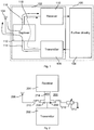
- Fig. 1 illustrates an example of a communication apparatus 100 comprising a transceiver 102, an antenna 104 connected to the transceiver 102, and further circuitry 106 such as processing means, input and output circuitry, and memory means.
- the transceiver 102 comprises a transmitter 108, a receiver 110, and a duplexer 112 which is connected to the transmitter 102, the receiver 110 and the antenna 104.
- the duplexer 112 is arranged to direct radio frequency (RF) signal from the transmitter to the antenna, as indicated by arrow 114, and from the antenna to the receiver, as indicated by arrow 116, and can for example comprise a circulator.
- RF radio frequency
- Duplexers are known in the art and for example described in US 4,325,140 . However, duplexers are not ideal and a leakage of transmitter signals from the transmitter to the receiver, as indicated by arrow 118, is at least to some degree present. Further, duplexers are commonly costly, space consuming and challenging to be implemented on-chip.
- FIG. 2 illustrates an example of such a structure 200, which is also disclosed in WO 2009/080878 A1 , comprising a transmitter 202, a receiver 204, and an antenna 206.
- the transmitter 202 provides its output signal both to a branch towards the antenna 206, the branch comprising a capacitor 208 and an inductor 210, and to a branch towards a dummy load 212, the branch comprising a capacitor 208' and an inductor 210'.
- the dummy load 212 is arranged to mimic the impedance of the antenna 206, and by the achieved symmetry, and, when using a differential input to the receiver 204 via a transformer 214, the contribution at the receiver input from the transmitted signal can be suppressed.
- a drawback of this solution is that half the signal energy is lost in the dummy load 212.
- Another drawback is that a transformer is necessary, which may be hard to implement at low cost and/or low space consumption, e.g. on chip.
- US 2013/176912 A1 discloses an RF duplexing devices including a transmission port, a receive port, a first duplexer, and a second duplexer.
- the first duplexer is coupled to the transmission port and the receive port, and is configured to provide a first phase shift from the transmission port to the receive port.
- the second duplexer is also coupled to the transmission port and the receive port.
- the second duplexer is configured to provide a second phase shift that is differential to the first phase shift from the transmission port to the receive port.
- the present invention is based on the understanding that counteracting contribution from a transmitter at a receiver input in a transceiver reduces or cancels the signal.
- the inventor has found that contribution by the transmitter signal at the receiver input can be further alleviated by a filtering structure and a phase shifter structure, wherein less transmitter energy is lost and the operation is independent of impedance changes at a transmission port for antenna connection.
- a transceiver arrangement comprising a receiver arranged for frequency-division duplex communication with a communication network and a transmitter arranged for frequency-division duplex communication with the communication network.
- the transceiver arrangement also comprises a transmission port for connecting to an antenna or a communication wire, and a phase shifter arrangement which comprises a first 180° phase shifter and a second 180'phase shifter.
- the transceiver arrangement further comprises a filtering arrangement.
- the filtering arrangement comprises filters of a first type and filters of a second type.
- the filtering arrangement and the phase shifter arrangement are arranged to connect the receiver, transmitter and transmission port forming a first signal path between the transmission port and the transmitter by a first one of the filters of the first type and the first phase shifter in series, a second signal path between the transmission port and the transmitter by a second one of the filters of the first type and a first one of the filters of the second type in series, a third signal path between the transmission port and the receiver by a second one of the filters of the second type and the second phase shifter in series, and a fourth signal path between the transmission port and the receiver by a third one of the filters of the second type and a third one of the filters of the first type in series.
- the filters of the first type are arranged to pass signals at transmitter frequency and attenuate signals at receiver frequency
- the filters of the second type are arranged to attenuate signals at transmitter frequency and pass signals at receiver frequency.
- the filters of the first and second types may be non-directional filters comprising linear components.
- the filters of the first type may each comprise a capacitance and a first inductance coupled in parallel where the parallel coupling is coupled in series with a second inductance
- the filters of the second type may each comprise a first capacitance and an inductance coupled in parallel, where the parallel coupling is coupled in series with a second capacitance.
- At least one of the capacitance and the first and second inductances of each of the filters of the first type may be controllable and be arranged to be controlled by a controller, and at least one of the inductance and the first and second capacitances of each of the filters of the second type may be controllable and be arranged to be controlled by the controller.
- the filters of the first type may each comprise a first capacitance and an inductance coupled in parallel, where the parallel coupling is coupled in series with a second capacitance
- the filters of the second type may each comprise a capacitance and a first inductance coupled in parallel where the parallel coupling is coupled in series with a second inductance.
- At least one of the inductance and the first and second capacitances of each of the filters of the first type may be controllable and be arranged to be controlled by a controller, and at least one of the capacitance and the first and second inductances of each of the filters of the second type may be controllable and be arranged to be controlled by the controller.
- At least one of the first and second phase shifters may comprise a transformer arrangement.
- the transformer arrangement may comprise a first winding connected between a first terminal of the transformer arrangement and a reference voltage and a second winding connected between a second terminal of the transformer arrangement and a reference voltage, wherein the first and second windings have mutually opposite magnetic polarity.
- the transformer arrangement may comprise an autotransformer with a winding connected between a first terminal of the transformer arrangement and a second terminal of the transformer arrangement, with a tap of the winding connected to a reference voltage.
- a communication device capable of frequency division duplex communication via a communication network, comprising a transceiver arrangement according to the first aspect.
- Fig. 3 is a block diagram which schematically illustrates a transceiver arrangement 300 according to an embodiment.
- the transceiver comprises a receiver 302 arranged for frequency-division duplex communication with a wireless or wired communication network, a transmitter 304 arranged for frequency-division duplex, FDD, communication with the wireless or wired communication network, and an antenna port 306 for connecting to an antenna.
- the term "antenna port” is used for easier understanding and is evident for the example of a wireless transceiver.
- the term can be substituted by for example the term "cable connection” to provide easier understanding of how the transceivers disclosed herein can be used for wired operation in all the herein given examples.
- a general term can be "transmission port", which should apply for both wired and wireless operation.
- the transmission port is arranged both for transmitting and receiving signals.
- the transceiver arrangement further comprises a phase shifter arrangement, which comprises a first 180° phase shifter 308 and a second 180° phase shifter 309, and a filtering arrangement, which comprises filters of a first type 310, 312, 314 and filters of a second type 316, 318, 320.
- Filters 310, 312, 314 are of a first type which are arranged to pass signals at transmitting frequency, i.e. the frequency at which the transmitter 304 transmits, and are arranged to attenuate signals at receiving frequency, i.e. the frequency at which the receiver 302 receives desired signals.
- the transmitting frequency and the receiving frequencies are distinguished since the transceiver 300 is arranged to work with FDD communication.
- Filters 316, 318, 320 are of a second type which are arranged to pass signals at the receiving frequency and attenuate signals at the transmitting frequency.
- the filtering arrangement and the phase shifter arrangement are arranged to connect the receiver 302, transmitter 304 and transmission port 306 forming a first signal path between the transmission port 306 and the transmitter 304 by a first one of the filters 310 of the first type and the first phase shifter 308 in series, a second signal path between the transmission port 306 and the transmitter 304 by a second one of the filters 312 of the first type and a first one of the filters 316 of the second type in series, a third signal path between the transmission port 306 and the receiver 302 by a second one of the filters 318 of the second type and the second phase shifter 309 in series, and a fourth signal path between the transmission port 306 and the receiver 302 by a third one of the filters 320 of the second type and a third one of the filters 314 of the first type in series.
- a signal at transmitting frequency from the transmitter 304 is passed via the first signal path towards the antenna port 306 such that it is enabled to be transmitted efficiently through an antenna connected to the transmission port 306.
- the signal at transmitting frequency from the transmitter 304 is also passed via the second signal path, where the signal is subject to both a filter of the second type 316 and a filter of the first type 312.
- the signal at the transmitting frequency is then attenuated by the filter of the second type 316, so that the amplitude of the transmitting signal at the transmission port 306 is not much affected by the second signal path.
- the transmitter noise i.e. the transmitter signals at receiving frequency, on the other hand will in both paths be attenuated by the filters of the first type 310, 312.
- the phase shifter 308 will make the signals from the two paths appear with opposite phase.
- attenuated transmitter noise at the receive frequency is provided by the two paths, but with opposite phase, and in addition to the attenuation by filtering, cancellation will further reduce the interference passed on to the receiver input.
- a received signal from an antenna connected to the transmission port 306 reaches the receiver 302 via the third signal path, i.e. via the filter 318 which passes the receiving signal but attenuates the transmit signal which also is present at the transmission port 306.
- the received signal is also passed via the fourth signal path, where the signal is subject to both at filter of the second type 320 and a filter of the first type 314.
- received signal at transmit frequency attenuated by the filters 318, 320 of the second type is provided by the two paths, but with opposite phase, further reducing the transmitter frequency contribution at the receiver input.
- Receiving frequency signals are attenuated by the filter of the first type 314 in the fourth path. The fourth path will thus have small impact on the receiving signal amplitude reaching the receiver 302.
- the transceiver 300 provides a structure which efficiently provides signals from the transmitter to the transmission port 306, efficiently provides signals from the transmission port to the receiver, and at the same time reduces both receiving and transmitting frequency signals from the transmitter reaching the receiver.
- Symmetry in receiving frequency attenuation between the first and second signal paths, and transmitting frequency attenuation between the third and fourth signal paths, respectively, is desired to keep the signals with opposite phase on equal levels to achieve cancelling as demonstrated above.
- phase and amplitude will track across a wide bandwidth, resulting in a wideband cancellation.
- the filter 316 of the second type has a rather flat frequency response at receiver frequency which is close to a constant loss.
- the loss at receiver frequency of the 180° phase shifter 308 equal to that of the filter 316, the cancellation demonstrated above will be effective and a high isolation at receiver frequency from the transmitter 304 will be achieved.
- the isolation is independent of antenna impedance of an antenna connected to the transmission port 306 since the receiver frequency current from the transmitter will be cancelled before building up a voltage in the antenna impedance.
- the filter 314 of the first type has a rather flat frequency response at transmitter frequency close to constant loss, and the loss at transmitter frequency of the 180° phase shifter equal is made equal to that of the filter 314.
- the isolation of signals at transmitter frequency at the transmission port 306 is also similarly independent on an antenna impedance of an antenna connected to the transmission port 306, and effective isolation is provided at transmitter frequencies from the transmission port 306 to the input of the receiver 302.
- the filters of the first type and filters of the second type are normally very consistent, and so are the phase shifters.
- the mutual agreement in loss between the respective paths may be trimmed by for example a resistor bank, which may be programmable, e.g. by burn switches.
- a controller 340 may be arranged to control the filters 310, 312 , 314, 316, 318, 320 such that suitable filter characteristics for passing and attenuating signals as described above are achieved for different constellations of frequencies for transmitting and receiving. For example, if the transceiver operates in FDD where transmit frequency is a certain amount higher than the receive frequency, and the transceiver switches to an operation mode where the transceiver operates in FDD and where the receive frequency is a certain amount higher than the transmit frequency, the controller 340 can swap the properties of filter the first and second types.
- “swap” means: if, in a first state receive signal frequency is higher than transmit signal frequency in the FDD, and upon transition to a second state where receive signal frequency is lower than transmit signal frequency in the FDD, the properties of the filters of first type will be assigned the properties of the filters of the second type as of the first state, and the filters of the second type will be assigned the properties of the filters of the first type as of the first state in sense of frequencies to pass and block.
- the frequency properties of the respective filter types may also be adapted to the second state, e.g. if other frequencies are applied in the second state.
- a change of respective properties of filters of first and second types can be made by the controller 340 upon change of the certain amount of frequency difference between receive and transmit frequencies, etc.
- signals from the controller are indicated as dotted arrows which indicate control signals provided from the controller 340.
- Fig. 4 is a block diagram schematically illustrating a communication device 400.
- the communication device 400 is capable of frequency division duplex communication via a communication network.
- the communication device 400 comprises a transceiver arrangement 402 according to any of the above demonstrated embodiments.
- the transceiver arrangement 402 is connected to an antenna 404 through its transmission port.
- the communication device can also comprise other circuits 406, such as interface towards a user and/or other circuitry or machines, memory, processor, etc.
- the communication device 400 can be a smartphone or cellphone, a communication card or device in or for a computer, an embedded communication device in a machine, or the like.
- the communication device 400 can be adapted for cellular communication, point-to-point communication, or for communication in a wireless or wired network.
- the transmission port described above need not necessarily by connected to an antenna, but can equally be connected to a wired line which conveys radio frequency signals.
- the communication device 400 described with reference to Fig. 4 need not comprise the antenna 404 wherein the communication device is instead connected to such a wired line conveying radio frequency signals.
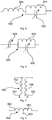
- Fig. 5 illustrates a filter 500 according to an embodiment, which provides dual resonance properties where high insertion loss is provided at one frequency and low insertion loss is provided at another frequency not far from the first frequency, which has been found a reasonable compromise for at least some of the embodiments. It comprises an inductance 504 coupled in parallel with a capacitance 502, wherein the parallel coupling 502, 504 is coupled in series with an inductance 506 between the input and output of the filter 500. It provides a parallel resonance, attenuating the signal at a frequency below a series resonance where the signal is passed.
- Fig. 6 illustrates a filter 600 according to an embodiment, which corresponds to the filter demonstrated with reference to Fig. 5 , but with the difference that the parallel coupling 602, 604 is coupled in series with a capacitance 606 between the input and output of the filter 600, and that it provides a series resonance frequency below the parallel resonance frequency.
- the filters of the first type can be selected as one of the types illustrated in Fig. 5 or 6 , and the filters of the second type are then selected as the other one of the types illustrated in Fig. 5 or 6 .
- an efficient way is to let the controller 340 control the capacitance values of capacitances 502, 602, 606 of the filters, e.g. by having the capacitances 502, 602, 606 as controllable capacitance banks. It is of course also possible to control inductors 506, 504, 604.
- Fig. 7 illustrates a 180° phase shifter 700 according to an embodiment.
- the transformer arrangement 700 comprises a first winding 702 connected between a first terminal of the transformer arrangement and a reference voltage 703 and a second winding 704 connected between a second terminal of the transformer arrangement and a reference voltage 705.
- the first and second windings are arranged to have mutually opposite magnetic polarity, wherein a signal provided at one of the terminals will provide a signal with opposite polarity, i.e. 180° phase shifted, on the other terminal.
- Fig. 8 illustrates a 180° phase shifter 800 according to an embodiment.
- the transformer arrangement 800 comprises an autotransformer with a winding 802 connected between a first terminal of the transformer arrangement a second terminal of the transformer arrangement, and a tap 804 connected to a reference voltage.
- the magnetic coupling of the winding 802 and the connection with the tap 804 to the reference voltage 803 provides for a signal provided at one of the terminals will provide a signal with opposite polarity, i.e. 180° phase shifted, on the other terminal.
Landscapes
- Engineering & Computer Science (AREA)
- Signal Processing (AREA)
- Computer Networks & Wireless Communication (AREA)
- Transceivers (AREA)
Claims (10)
- Agencement émetteur-récepteur (300, 402) comprenant :un récepteur (302) agencé pour une communication à duplexage par répartition de fréquence avec un réseau de communication ;un émetteur (304) agencé pour une communication à duplexage par répartition de fréquence avec le réseau de communication ;un port de transmission (306) ;un agencement déphaseur comprenant un premier déphaseur de 180° (308) et un deuxième déphaseur de 180° (309) ; etun agencement de filtrage comprenant des filtres d'un premier type (310, 312, 314) et des filtres d'un deuxième type (316, 318, 320),dans lequel l'agencement de filtrage et l'agencement déphaseur sont agencés pour raccorder le récepteur (302), l'émetteur (304) et le port de transmission (306) en constituant :une première voie de signal entre le port de transmission (306) et l'émetteur (304) par un premier des filtres (310) du premier type et le premier déphaseur (308) en série ;une deuxième voie de signal entre le port de transmission (306) et l'émetteur (304) par un deuxième des filtres (312) du premier type et un premier des filtres (316) du deuxième type en série ;une troisième voie de signal entre le port de transmission (306) et le récepteur (302) par un deuxième des filtres (318) du deuxième type et le deuxième déphaseur (309) en série ;une quatrième voie de signal entre le port de transmission (306) et le récepteur (302) par un troisième des filtres (320) du deuxième type et un troisième des filtres (314) du premier type en série,et dans lequelles filtres du premier type (310, 312, 314) sont agencés pour laisser passer des signaux à une fréquence d'émetteur et atténuer des signaux à une fréquence de récepteur, et les filtres du deuxième type (316, 318, 320) sont agencés pour atténuer des signaux à une fréquence d'émetteur et laisser passer des signaux à une fréquence de récepteur.
- Agencement émetteur-récepteur selon la revendication 1, dans lequel les filtres du premier type et du deuxième type sont des filtres non directionnels comprenant des composants linéaires.
- Agencement émetteur-récepteur (300, 402) selon l'une quelconque des revendications précédentes, dans lequel chacun des filtres du premier type (310, 312, 314) comprend une capacité (502) et une première inductance (504) couplées en parallèle, où le couplage en parallèle est couplé en série à une deuxième inductance (506), et chacun des filtres du deuxième type (316, 318, 320) comprend une première capacité (602) et une inductance (604) couplées en parallèle, où le couplage en parallèle est couplé en série à une deuxième capacité (606).
- Agencement émetteur-récepteur (300, 402) selon la revendication 3, dans lequel au moins l'une de la capacité (502) et des première et deuxième inductances (504, 506) de chacun des filtres du premier type (310, 312, 314) peut être commandée et est agencée pour être commandée par un organe de commande (340), et au moins l'une de l'inductance (604) et des première et deuxième capacités (602, 606) de chacun des filtres du deuxième type (316, 318, 320) peut être commandée et est agencée pour être commandée par l'organe de commande (340).
- Agencement émetteur-récepteur (300, 402) selon l'une quelconque des revendications 1 et 2, dans lequel chacun des filtres du premier type (310, 312, 314) comprend une première capacité (602) et une inductance (604) couplées en parallèle, où le couplage en parallèle est couplé en série à une deuxième capacité (606), et chacun des filtres du deuxième type (316, 318, 320) comprend une capacité (502) et une première inductance (504) couplées en parallèle, où le couplage en parallèle est couplé en série à une deuxième inductance (506).
- Agencement émetteur-récepteur (300, 402) selon la revendication 5, dans lequel au moins l'une de l'inductance (604) et des première et deuxième capacités (602, 606) de chacun des filtres du premier type (310, 312, 314) peut être commandée et est agencée pour être commandée par un organe de commande (340), et au moins l'une de la capacité (502) et des première et deuxième inductances (504, 506) de chacun des filtres du deuxième type (316, 318, 320) peut être commandée et est agencée pour être commandée par l'organe de commande (340).
- Agencement émetteur-récepteur (300, 402) selon l'une quelconque des revendications précédentes, dans lequel au moins l'un des premier et deuxième déphaseurs comprend un agencement transformateur (700, 800).
- Agencement émetteur-récepteur (300, 403) selon la revendication 7, dans lequel l'agencement transformateur (700) comprend un premier enroulement (702) raccordé entre une première borne de l'agencement transformateur et une tension de référence (703) et un deuxième enroulement (704) raccordé entre une deuxième borne de l'agencement transformateur et une tension de référence (705), dans lequel les premier et deuxième enroulements ont une polarité magnétique mutuellement opposée.
- Agencement émetteur-récepteur (300, 403) selon la revendication 7, dans lequel l'agencement transformateur (800) comprend un autotransformateur avec un enroulement (802) raccordé entre une première borne de l'agencement transformateur et une deuxième borne de l'agencement transformateur, avec une prise (804) de l'enroulement (802) raccordée à une tension de référence (803).
- Dispositif de communication (400), capable d'effectuer une communication à duplex sage par répartition de fréquences par l'intermédiaire d'un réseau de communication, comprenant un agencement émetteur-récepteur (402) selon l'une quelconque des revendications 1 à 9.
Applications Claiming Priority (1)
| Application Number | Priority Date | Filing Date | Title |
|---|---|---|---|
| PCT/EP2014/051155 WO2015110149A1 (fr) | 2014-01-21 | 2014-01-21 | Montage émetteur-récepteur et dispositif de communication |
Publications (2)
| Publication Number | Publication Date |
|---|---|
| EP3097645A1 EP3097645A1 (fr) | 2016-11-30 |
| EP3097645B1 true EP3097645B1 (fr) | 2017-08-23 |
Family
ID=49999953
Family Applications (1)
| Application Number | Title | Priority Date | Filing Date |
|---|---|---|---|
| EP14701074.8A Active EP3097645B1 (fr) | 2014-01-21 | 2014-01-21 | Montage émetteur-récepteur et dispositif de communication |
Country Status (3)
| Country | Link |
|---|---|
| US (1) | US9900044B2 (fr) |
| EP (1) | EP3097645B1 (fr) |
| WO (1) | WO2015110149A1 (fr) |
Families Citing this family (16)
| Publication number | Priority date | Publication date | Assignee | Title |
|---|---|---|---|---|
| FI4002724T3 (fi) | 2015-12-13 | 2025-09-30 | Gxc Llc | Häiriönpoistomenetelmiä ja -laite |
| US10257746B2 (en) * | 2016-07-16 | 2019-04-09 | GenXComm, Inc. | Interference cancellation methods and apparatus |
| WO2018145758A1 (fr) * | 2017-02-10 | 2018-08-16 | Telefonaktiebolaget Lm Ericsson (Publ) | Circuit d'isolement intégré dans un émetteur-récepteur duplex à répartition dans le temps |
| WO2019192728A1 (fr) * | 2018-04-06 | 2019-10-10 | Huawei Technologies Co., Ltd. | Agencement de filtre duplex à annulation de fuite |
| KR20210018480A (ko) | 2018-06-11 | 2021-02-17 | 더 트러스티이스 오브 콜롬비아 유니버시티 인 더 시티 오브 뉴욕 | 복수의 상쇄 경로를 포함하는 순환기를 위한 회로 및 방법 |
| US11150409B2 (en) | 2018-12-27 | 2021-10-19 | GenXComm, Inc. | Saw assisted facet etch dicing |
| WO2020150745A1 (fr) | 2019-01-19 | 2020-07-23 | The Trustees Of Columbia University In The City Of New York | Circuits non réciproques exempts de champ magnétique basés sur une modulation de conductance spatio-temporelle sous-harmonique |
| US10727945B1 (en) | 2019-07-15 | 2020-07-28 | GenXComm, Inc. | Efficiently combining multiple taps of an optical filter |
| US11215755B2 (en) | 2019-09-19 | 2022-01-04 | GenXComm, Inc. | Low loss, polarization-independent, large bandwidth mode converter for edge coupling |
| US11539394B2 (en) | 2019-10-29 | 2022-12-27 | GenXComm, Inc. | Self-interference mitigation in in-band full-duplex communication systems |
| US11606115B2 (en) * | 2019-11-12 | 2023-03-14 | Blue Danube Systems, Inc. | Transmitter signal cancellation in phased array receivers |
| US11796737B2 (en) | 2020-08-10 | 2023-10-24 | GenXComm, Inc. | Co-manufacturing of silicon-on-insulator waveguides and silicon nitride waveguides for hybrid photonic integrated circuits |
| US12001065B1 (en) | 2020-11-12 | 2024-06-04 | ORCA Computing Limited | Photonics package with tunable liquid crystal lens |
| WO2022178182A1 (fr) | 2021-02-18 | 2022-08-25 | GenXComm, Inc. | Maximisation de l'efficacité de systèmes de communication avec des sous-systèmes d'annulation d'auto-interférences |
| EP4331120A1 (fr) | 2021-04-29 | 2024-03-06 | Genxcomm, Inc. | Sous-systèmes d'annulation d'auto-interférence pour noeuds de réseau maillé |
| US11838056B2 (en) | 2021-10-25 | 2023-12-05 | GenXComm, Inc. | Hybrid photonic integrated circuits for ultra-low phase noise signal generators |
Family Cites Families (82)
| Publication number | Priority date | Publication date | Assignee | Title |
|---|---|---|---|---|
| US404375A (en) | 1889-06-04 | Egbert e | ||
| US3900823A (en) | 1973-03-28 | 1975-08-19 | Nathan O Sokal | Amplifying and processing apparatus for modulated carrier signals |
| US4325140A (en) | 1978-10-06 | 1982-04-13 | The United States Of America As Represented By The Scretary Of The Air Force | Full duplex communication system apparatus using frequency selective limiters |
| US5057342A (en) | 1987-12-21 | 1991-10-15 | Union Carbide Chemicals And Plastics Technology Corporation | Methods and apparatus for obtaining a feathered spray when spraying liquids by airless techniques |
| US5404375A (en) | 1993-08-23 | 1995-04-04 | Westinghouse Electric Corp. | Process and apparatus for satellite data communication |
| US6169912B1 (en) | 1999-03-31 | 2001-01-02 | Pericom Semiconductor Corp. | RF front-end with signal cancellation using receiver signal to eliminate duplexer for a cordless phone |
| KR100360895B1 (ko) | 1999-11-23 | 2002-11-13 | 주식회사 텔웨이브 | 서큘레이터를 이용한 송/수신부 결합 시스템 및 그의송신신호 소거방법 |
| WO2002017506A1 (fr) | 2000-08-22 | 2002-02-28 | Novatel Wireless, Inc. | Procede et dispositif de suppression de bruit d'emetteur dans un systeme de telecommunications hf |
| US6745018B1 (en) | 2000-09-29 | 2004-06-01 | Intel Corporation | Active cancellation of a wireless coupled transmit signal |
| US6845126B2 (en) * | 2001-01-26 | 2005-01-18 | Telefonaktiebolaget L.M. Ericsson (Publ) | System and method for adaptive antenna impedance matching |
| JP3772771B2 (ja) | 2001-05-18 | 2006-05-10 | 松下電器産業株式会社 | マルチバンド高周波スイッチ |
| US6670866B2 (en) | 2002-01-09 | 2003-12-30 | Nokia Corporation | Bulk acoustic wave resonator with two piezoelectric layers as balun in filters and duplexers |
| KR101031692B1 (ko) | 2002-12-18 | 2011-04-29 | 파나소닉 주식회사 | 무선 통신 장치, 무선 통신 방법, 안테나 장치 및 제 1듀플렉서 |
| RU2264032C2 (ru) | 2003-04-17 | 2005-11-10 | Федеральное государственное унитарное предприятие Омский научно-исследовательский институт приборостроения | Приемопередатчик |
| EP1480333A3 (fr) | 2003-05-22 | 2006-05-03 | Matsushita Electric Industrial Co., Ltd. | Amplificateur différentiel à haute fréquence, mélangeur différentiel, oscillateur différentiel et circuit radio les utilisant |
| EP1515450B1 (fr) | 2003-08-15 | 2007-08-15 | TDK Corporation | Circuit de commutation d'antenne |
| US7081831B2 (en) | 2003-08-29 | 2006-07-25 | Halliburton Energy Services, Inc. | Time-domain signal cancellation in downhole telemetry systems |
| US7369096B2 (en) | 2003-10-10 | 2008-05-06 | Broadcom Corporation | Impedance matched passive radio frequency transmit/receive switch |
| US7155178B2 (en) | 2004-01-29 | 2006-12-26 | Mediatek Inc. | Circuit system for wireless communications |
| US7446629B2 (en) | 2004-08-04 | 2008-11-04 | Matsushita Electric Industrial Co., Ltd. | Antenna duplexer, and RF module and communication apparatus using the same |
| JP2008521280A (ja) | 2004-11-15 | 2008-06-19 | クゥアルコム・インコーポレイテッド | 送信漏れ信号除去用適応フィルタ |
| US7738654B2 (en) | 2004-12-02 | 2010-06-15 | Solarflare Communications, Inc. | Isolation of transmit and receive signals |
| TW200625799A (en) | 2004-12-22 | 2006-07-16 | Airoha Tech Corp | RF front-end structure |
| US8364092B2 (en) | 2005-04-14 | 2013-01-29 | Ecole De Technologie Superieure | Balanced active and passive duplexers |
| JP4713939B2 (ja) | 2005-05-19 | 2011-06-29 | ルネサスエレクトロニクス株式会社 | 電圧制御発振器及びそれを用いた無線通信機 |
| WO2007002273A2 (fr) | 2005-06-22 | 2007-01-04 | Knox Michael E | Reseau d'alimentation d'antennes pour communication en duplex integral |
| US7801493B2 (en) | 2005-11-23 | 2010-09-21 | Trex Enterprises Corp. | Quasi-circulator for antenna multi-coupler system |
| US7865159B2 (en) | 2006-01-27 | 2011-01-04 | Qualcomm Incorporated | Repeater rise-over-thermal (RoT) value calibration |
| KR101238359B1 (ko) | 2006-02-06 | 2013-03-04 | 삼성전자주식회사 | 듀플렉서 |
| US20070207747A1 (en) | 2006-03-06 | 2007-09-06 | Paul Johnson | Single frequency duplex radio link |
| EP1835630A1 (fr) | 2006-03-17 | 2007-09-19 | STMicroelectronics N.V. | Procédé de minimisation de la fuite de signal dans un système du type à transmission bi-directionnelle simultanée, et dispositif correspondant |
| US7894779B2 (en) | 2006-06-22 | 2011-02-22 | Honeywell International Inc. | Apparatus and method for transmitting and receiving multiple radio signals over a single antenna |
| JP2008186530A (ja) | 2007-01-30 | 2008-08-14 | Toshiba Corp | 情報記憶媒体及び情報記録方法並びに情報再生方法 |
| US7756480B2 (en) | 2007-02-16 | 2010-07-13 | Samsung Electronics Co., Ltd. | System and method for transmitter leak-over cancellation |
| US7983627B2 (en) | 2007-03-30 | 2011-07-19 | Infineon Technologies Ag | Circuit arrangement with improved decoupling |
| US7917096B2 (en) | 2007-03-30 | 2011-03-29 | Sony Ericsson Mobile Communications Ab | Antenna interface circuits including multiple impedance matching networks that are respectively associated with multiple frequency bands and electronic devices incorporating the same |
| US20080279262A1 (en) | 2007-05-07 | 2008-11-13 | Broadcom Corporation | On chip transmit/receive selection |
| JP5229969B2 (ja) | 2007-08-23 | 2013-07-03 | 太陽誘電株式会社 | デュープレクサ、通信モジュール、および通信装置 |
| WO2009078095A1 (fr) | 2007-12-18 | 2009-06-25 | Fujitsu Limited | Duplexeur, module comprenant le duplexeur et dispositif de communication |
| FI20075942A7 (fi) | 2007-12-20 | 2009-06-21 | Valtion Teknillinen Tutkimuskeskus | RFID-lukulaite ja menetelmä RFID-lukulaitteessa |
| US8351874B2 (en) | 2008-04-08 | 2013-01-08 | Telefonaktiebolaget Lm Ericsson (Publ) | System and method for adaptive antenna impedance matching |
| JP2009284412A (ja) | 2008-05-26 | 2009-12-03 | Nec Electronics Corp | 無線通信装置 |
| WO2010010425A1 (fr) | 2008-07-25 | 2010-01-28 | Freescale Semiconductor, Inc. | Récepteur hétérodyne |
| US8208866B2 (en) | 2008-08-05 | 2012-06-26 | Broadcom Corporation | RF transceiver front-end with RX/TX isolation |
| DE102008045346B4 (de) | 2008-09-01 | 2018-06-07 | Snaptrack Inc. | Duplexer und Verfahren zum Erhöhen der Isolation zwischen zwei Filtern |
| EP2226948B1 (fr) | 2009-03-03 | 2015-07-29 | Qualcomm Technologies, Inc. | Système de communication et procédé pour la transmission et la réception de signaux |
| US20100279617A1 (en) | 2009-04-30 | 2010-11-04 | Matsushita Electric Industrial Co., Ltd. | Methods and Apparatus for Reducing Receive Band Noise in Communications Transceivers |
| KR101553007B1 (ko) | 2009-05-27 | 2015-09-15 | 한화테크윈 주식회사 | 송신 누설 신호 제거 장치 및 방법 |
| US8897722B2 (en) | 2009-09-11 | 2014-11-25 | Broadcom Corporation | RF front-end with wideband transmitter/receiver isolation |
| US8208865B2 (en) | 2009-09-11 | 2012-06-26 | Broadcom Corporation | RF front-end with on-chip transmitter/receiver isolation and noise-matched LNA |
| US9543661B2 (en) | 2009-11-09 | 2017-01-10 | Tyco Electronics Services Gmbh | RF module and antenna systems |
| US8269522B2 (en) | 2009-12-14 | 2012-09-18 | St-Ericsson Sa | Active eye opener for current-source driven, high-speed serial links |
| US8514035B2 (en) | 2009-12-30 | 2013-08-20 | Broadcom Corporation | RF front-end with on-chip transmitter/receiver isolation using a gyrator |
| US8489040B2 (en) | 2010-02-18 | 2013-07-16 | Telefonaktiebolaget L M Ericsson (Publ) | Double clipped RF clock generation with spurious tone cancellation |
| EP2572451B1 (fr) | 2010-05-17 | 2017-07-12 | Tyco Electronics Services GmbH | Duplexeur doté d'une isolation améliorée |
| KR101386839B1 (ko) | 2010-05-18 | 2014-04-18 | 엘에스산전 주식회사 | Rfid 시스템의 송신누설신호 제거장치 |
| US8792836B2 (en) | 2010-06-03 | 2014-07-29 | Broadcom Corporation | Front end module with compensating duplexer |
| US8725085B2 (en) | 2010-06-03 | 2014-05-13 | Broadcom Corporation | RF front-end module |
| WO2012005787A1 (fr) | 2010-07-08 | 2012-01-12 | Microsemi Corporation | Architecture améliorée pour coexistence de radios à plusieurs bandes |
| US8654743B1 (en) | 2010-10-29 | 2014-02-18 | Lilee Systems, Ltd | Device and method for configurable transmit and receive antennas |
| JP5570954B2 (ja) | 2010-11-24 | 2014-08-13 | 富士通株式会社 | 発振回路 |
| US8798546B2 (en) | 2011-01-31 | 2014-08-05 | Telcordia Technologies, Inc. | Directional filter for separating closely spaced channels in an HF transceiver |
| US8975981B2 (en) | 2011-09-13 | 2015-03-10 | Qualcomm Incorporated | Impedance matching circuits with multiple configurations |
| US8923167B2 (en) | 2011-09-27 | 2014-12-30 | Google Technology Holdings LLC | Communication device for simultaneous transmission by multiple transceivers |
| US9319208B2 (en) * | 2012-01-10 | 2016-04-19 | Rf Micro Devices, Inc. | RF duplexing device |
| EP2621097B1 (fr) | 2012-01-26 | 2015-09-16 | Telefonaktiebolaget L M Ericsson (publ) | Émetteur/récepteur, procédé, programme informatique et dispositif de communication |
| EP2621098B1 (fr) | 2012-01-30 | 2015-07-01 | Telefonaktiebolaget L M Ericsson (Publ) | Émetteur-récepteur et dispositif de communication |
| US8971219B2 (en) * | 2012-03-30 | 2015-03-03 | Qualcomm Incorporated | Hybrid transformer based integrated duplexer for multi-band/multi-mode radio frequency (RF) front end |
| US9445480B2 (en) | 2012-04-12 | 2016-09-13 | Lg Electronics Inc. | Lighting system, lighting apparatus, and lighting control method |
| TWI462497B (zh) | 2012-05-23 | 2014-11-21 | Wistron Neweb Corp | 射頻電路系統及改善射頻電路系統的隔離度的方法 |
| ES2533314T3 (es) * | 2012-06-07 | 2015-04-09 | Telefonaktiebolaget L M Ericsson (Publ) | Transceptor sin duplexor y aparato de comunicación |
| CN104604144A (zh) | 2012-07-09 | 2015-05-06 | 瑞典爱立信有限公司 | 收发器前端 |
| EP2912871A4 (fr) | 2012-10-29 | 2016-06-15 | Ericsson Telefon Ab L M | Partage en temps d'un spectre de fréquences entre opérateurs |
| EP2733855B1 (fr) | 2012-11-15 | 2016-07-27 | Telefonaktiebolaget LM Ericsson (publ) | Module frontal émetteur-récepteur |
| CN105103462A (zh) | 2012-12-11 | 2015-11-25 | 南加利福尼亚大学 | 用于双工器和共存无线通信系统的无源泄露抵消网络 |
| US8830881B2 (en) * | 2012-12-14 | 2014-09-09 | Broadcom Corporation | Wide band electrical balance duplexer with balanced bridge circuit |
| US9000860B2 (en) | 2012-12-18 | 2015-04-07 | Broadcom Corporation | Low-loss TX-to-RX isolation using electrical balance duplexer with noise cancellation |
| US8872587B2 (en) | 2013-03-06 | 2014-10-28 | International Business Machines Corporation | Generating negative impedance compensation |
| BR112015022333B1 (pt) | 2013-03-14 | 2022-08-23 | Telefonaktiebolaget L M Ericsson (Publ) | Transceptor, e, dispositivo de comunicação |
| US9577683B2 (en) | 2013-04-22 | 2017-02-21 | University Of Washington Through Its Center For Commercialization | Systems, transceivers, receivers, and methods including cancellation circuits having multiport transformers |
| BR112015026916B1 (pt) | 2013-04-26 | 2022-07-05 | Telefonaktiebolaget L M Ericsson (Publ) | Arranjo de transceptor, dispositivo de comunicação, método para controlar um arranjo de transceptor, e, meio de armazenamento legível por computador |
| WO2014177191A1 (fr) | 2013-04-30 | 2014-11-06 | Telefonaktiebolaget L M Ericsson (Publ) | Agencement d'émetteur-récepteur, dispositif de communication, procédé et programme informatique |
-
2014
- 2014-01-21 EP EP14701074.8A patent/EP3097645B1/fr active Active
- 2014-01-21 WO PCT/EP2014/051155 patent/WO2015110149A1/fr not_active Ceased
- 2014-01-21 US US15/113,342 patent/US9900044B2/en active Active
Non-Patent Citations (1)
| Title |
|---|
| None * |
Also Published As
| Publication number | Publication date |
|---|---|
| US9900044B2 (en) | 2018-02-20 |
| WO2015110149A1 (fr) | 2015-07-30 |
| US20170005696A1 (en) | 2017-01-05 |
| EP3097645A1 (fr) | 2016-11-30 |
Similar Documents
| Publication | Publication Date | Title |
|---|---|---|
| EP3097645B1 (fr) | Montage émetteur-récepteur et dispositif de communication | |
| EP2989724B1 (fr) | Dispositif émetteur-récepteur, dispositif de communication, procédé et programme informatique | |
| EP2672631B1 (fr) | Émetteur-récepteur sans duplexeur et appareil de communication | |
| US10348356B2 (en) | Transmitter receiver leakage reduction in a full duplex system without the use of a duplexer | |
| EP2992614B1 (fr) | Dispositif émetteur-récepteur, dispositif de communication, procédé et programme informatique | |
| US10623048B2 (en) | Transceiver arrangement and communication device | |
| US10128815B2 (en) | Branching device | |
| EP2621098B1 (fr) | Émetteur-récepteur et dispositif de communication | |
| CN107735955A (zh) | 高频前端电路 | |
| US11855679B2 (en) | Antenna interface arrangement | |
| EP3053276B1 (fr) | Agencement d'émetteur-récepteur, dispositif de communication et procédé |
Legal Events
| Date | Code | Title | Description |
|---|---|---|---|
| PUAI | Public reference made under article 153(3) epc to a published international application that has entered the european phase |
Free format text: ORIGINAL CODE: 0009012 |
|
| 17P | Request for examination filed |
Effective date: 20160629 |
|
| AK | Designated contracting states |
Kind code of ref document: A1 Designated state(s): AL AT BE BG CH CY CZ DE DK EE ES FI FR GB GR HR HU IE IS IT LI LT LU LV MC MK MT NL NO PL PT RO RS SE SI SK SM TR |
|
| AX | Request for extension of the european patent |
Extension state: BA ME |
|
| DAX | Request for extension of the european patent (deleted) | ||
| GRAP | Despatch of communication of intention to grant a patent |
Free format text: ORIGINAL CODE: EPIDOSNIGR1 |
|
| INTG | Intention to grant announced |
Effective date: 20170529 |
|
| GRAS | Grant fee paid |
Free format text: ORIGINAL CODE: EPIDOSNIGR3 |
|
| GRAA | (expected) grant |
Free format text: ORIGINAL CODE: 0009210 |
|
| AK | Designated contracting states |
Kind code of ref document: B1 Designated state(s): AL AT BE BG CH CY CZ DE DK EE ES FI FR GB GR HR HU IE IS IT LI LT LU LV MC MK MT NL NO PL PT RO RS SE SI SK SM TR |
|
| REG | Reference to a national code |
Ref country code: GB Ref legal event code: FG4D |
|
| REG | Reference to a national code |
Ref country code: CH Ref legal event code: EP |
|
| REG | Reference to a national code |
Ref country code: AT Ref legal event code: REF Ref document number: 922328 Country of ref document: AT Kind code of ref document: T Effective date: 20170915 |
|
| REG | Reference to a national code |
Ref country code: IE Ref legal event code: FG4D |
|
| REG | Reference to a national code |
Ref country code: DE Ref legal event code: R096 Ref document number: 602014013455 Country of ref document: DE |
|
| REG | Reference to a national code |
Ref country code: NL Ref legal event code: MP Effective date: 20170823 |
|
| REG | Reference to a national code |
Ref country code: LT Ref legal event code: MG4D |
|
| REG | Reference to a national code |
Ref country code: AT Ref legal event code: MK05 Ref document number: 922328 Country of ref document: AT Kind code of ref document: T Effective date: 20170823 |
|
| REG | Reference to a national code |
Ref country code: FR Ref legal event code: PLFP Year of fee payment: 5 |
|
| PG25 | Lapsed in a contracting state [announced via postgrant information from national office to epo] |
Ref country code: AT Free format text: LAPSE BECAUSE OF FAILURE TO SUBMIT A TRANSLATION OF THE DESCRIPTION OR TO PAY THE FEE WITHIN THE PRESCRIBED TIME-LIMIT Effective date: 20170823 Ref country code: HR Free format text: LAPSE BECAUSE OF FAILURE TO SUBMIT A TRANSLATION OF THE DESCRIPTION OR TO PAY THE FEE WITHIN THE PRESCRIBED TIME-LIMIT Effective date: 20170823 Ref country code: NL Free format text: LAPSE BECAUSE OF FAILURE TO SUBMIT A TRANSLATION OF THE DESCRIPTION OR TO PAY THE FEE WITHIN THE PRESCRIBED TIME-LIMIT Effective date: 20170823 Ref country code: SE Free format text: LAPSE BECAUSE OF FAILURE TO SUBMIT A TRANSLATION OF THE DESCRIPTION OR TO PAY THE FEE WITHIN THE PRESCRIBED TIME-LIMIT Effective date: 20170823 Ref country code: NO Free format text: LAPSE BECAUSE OF FAILURE TO SUBMIT A TRANSLATION OF THE DESCRIPTION OR TO PAY THE FEE WITHIN THE PRESCRIBED TIME-LIMIT Effective date: 20171123 Ref country code: FI Free format text: LAPSE BECAUSE OF FAILURE TO SUBMIT A TRANSLATION OF THE DESCRIPTION OR TO PAY THE FEE WITHIN THE PRESCRIBED TIME-LIMIT Effective date: 20170823 Ref country code: LT Free format text: LAPSE BECAUSE OF FAILURE TO SUBMIT A TRANSLATION OF THE DESCRIPTION OR TO PAY THE FEE WITHIN THE PRESCRIBED TIME-LIMIT Effective date: 20170823 |
|
| PG25 | Lapsed in a contracting state [announced via postgrant information from national office to epo] |
Ref country code: BG Free format text: LAPSE BECAUSE OF FAILURE TO SUBMIT A TRANSLATION OF THE DESCRIPTION OR TO PAY THE FEE WITHIN THE PRESCRIBED TIME-LIMIT Effective date: 20171123 Ref country code: RS Free format text: LAPSE BECAUSE OF FAILURE TO SUBMIT A TRANSLATION OF THE DESCRIPTION OR TO PAY THE FEE WITHIN THE PRESCRIBED TIME-LIMIT Effective date: 20170823 Ref country code: IS Free format text: LAPSE BECAUSE OF FAILURE TO SUBMIT A TRANSLATION OF THE DESCRIPTION OR TO PAY THE FEE WITHIN THE PRESCRIBED TIME-LIMIT Effective date: 20171223 Ref country code: GR Free format text: LAPSE BECAUSE OF FAILURE TO SUBMIT A TRANSLATION OF THE DESCRIPTION OR TO PAY THE FEE WITHIN THE PRESCRIBED TIME-LIMIT Effective date: 20171124 Ref country code: LV Free format text: LAPSE BECAUSE OF FAILURE TO SUBMIT A TRANSLATION OF THE DESCRIPTION OR TO PAY THE FEE WITHIN THE PRESCRIBED TIME-LIMIT Effective date: 20170823 Ref country code: ES Free format text: LAPSE BECAUSE OF FAILURE TO SUBMIT A TRANSLATION OF THE DESCRIPTION OR TO PAY THE FEE WITHIN THE PRESCRIBED TIME-LIMIT Effective date: 20170823 Ref country code: PL Free format text: LAPSE BECAUSE OF FAILURE TO SUBMIT A TRANSLATION OF THE DESCRIPTION OR TO PAY THE FEE WITHIN THE PRESCRIBED TIME-LIMIT Effective date: 20170823 |
|
| PG25 | Lapsed in a contracting state [announced via postgrant information from national office to epo] |
Ref country code: CZ Free format text: LAPSE BECAUSE OF FAILURE TO SUBMIT A TRANSLATION OF THE DESCRIPTION OR TO PAY THE FEE WITHIN THE PRESCRIBED TIME-LIMIT Effective date: 20170823 Ref country code: DK Free format text: LAPSE BECAUSE OF FAILURE TO SUBMIT A TRANSLATION OF THE DESCRIPTION OR TO PAY THE FEE WITHIN THE PRESCRIBED TIME-LIMIT Effective date: 20170823 |
|
| REG | Reference to a national code |
Ref country code: DE Ref legal event code: R097 Ref document number: 602014013455 Country of ref document: DE |
|
| PG25 | Lapsed in a contracting state [announced via postgrant information from national office to epo] |
Ref country code: SK Free format text: LAPSE BECAUSE OF FAILURE TO SUBMIT A TRANSLATION OF THE DESCRIPTION OR TO PAY THE FEE WITHIN THE PRESCRIBED TIME-LIMIT Effective date: 20170823 Ref country code: EE Free format text: LAPSE BECAUSE OF FAILURE TO SUBMIT A TRANSLATION OF THE DESCRIPTION OR TO PAY THE FEE WITHIN THE PRESCRIBED TIME-LIMIT Effective date: 20170823 Ref country code: IT Free format text: LAPSE BECAUSE OF FAILURE TO SUBMIT A TRANSLATION OF THE DESCRIPTION OR TO PAY THE FEE WITHIN THE PRESCRIBED TIME-LIMIT Effective date: 20170823 Ref country code: SM Free format text: LAPSE BECAUSE OF FAILURE TO SUBMIT A TRANSLATION OF THE DESCRIPTION OR TO PAY THE FEE WITHIN THE PRESCRIBED TIME-LIMIT Effective date: 20170823 |
|
| PLBE | No opposition filed within time limit |
Free format text: ORIGINAL CODE: 0009261 |
|
| STAA | Information on the status of an ep patent application or granted ep patent |
Free format text: STATUS: NO OPPOSITION FILED WITHIN TIME LIMIT |
|
| 26N | No opposition filed |
Effective date: 20180524 |
|
| PG25 | Lapsed in a contracting state [announced via postgrant information from national office to epo] |
Ref country code: SI Free format text: LAPSE BECAUSE OF FAILURE TO SUBMIT A TRANSLATION OF THE DESCRIPTION OR TO PAY THE FEE WITHIN THE PRESCRIBED TIME-LIMIT Effective date: 20170823 |
|
| REG | Reference to a national code |
Ref country code: CH Ref legal event code: PL |
|
| PG25 | Lapsed in a contracting state [announced via postgrant information from national office to epo] |
Ref country code: LU Free format text: LAPSE BECAUSE OF NON-PAYMENT OF DUE FEES Effective date: 20180121 |
|
| REG | Reference to a national code |
Ref country code: IE Ref legal event code: MM4A |
|
| REG | Reference to a national code |
Ref country code: BE Ref legal event code: MM Effective date: 20180131 |
|
| PG25 | Lapsed in a contracting state [announced via postgrant information from national office to epo] |
Ref country code: CH Free format text: LAPSE BECAUSE OF NON-PAYMENT OF DUE FEES Effective date: 20180131 Ref country code: LI Free format text: LAPSE BECAUSE OF NON-PAYMENT OF DUE FEES Effective date: 20180131 Ref country code: BE Free format text: LAPSE BECAUSE OF NON-PAYMENT OF DUE FEES Effective date: 20180131 |
|
| PG25 | Lapsed in a contracting state [announced via postgrant information from national office to epo] |
Ref country code: IE Free format text: LAPSE BECAUSE OF NON-PAYMENT OF DUE FEES Effective date: 20180121 |
|
| PG25 | Lapsed in a contracting state [announced via postgrant information from national office to epo] |
Ref country code: MC Free format text: LAPSE BECAUSE OF FAILURE TO SUBMIT A TRANSLATION OF THE DESCRIPTION OR TO PAY THE FEE WITHIN THE PRESCRIBED TIME-LIMIT Effective date: 20170823 |
|
| PG25 | Lapsed in a contracting state [announced via postgrant information from national office to epo] |
Ref country code: MT Free format text: LAPSE BECAUSE OF NON-PAYMENT OF DUE FEES Effective date: 20180121 |
|
| PG25 | Lapsed in a contracting state [announced via postgrant information from national office to epo] |
Ref country code: TR Free format text: LAPSE BECAUSE OF FAILURE TO SUBMIT A TRANSLATION OF THE DESCRIPTION OR TO PAY THE FEE WITHIN THE PRESCRIBED TIME-LIMIT Effective date: 20170823 |
|
| PG25 | Lapsed in a contracting state [announced via postgrant information from national office to epo] |
Ref country code: PT Free format text: LAPSE BECAUSE OF FAILURE TO SUBMIT A TRANSLATION OF THE DESCRIPTION OR TO PAY THE FEE WITHIN THE PRESCRIBED TIME-LIMIT Effective date: 20170823 |
|
| PG25 | Lapsed in a contracting state [announced via postgrant information from national office to epo] |
Ref country code: MK Free format text: LAPSE BECAUSE OF NON-PAYMENT OF DUE FEES Effective date: 20170823 Ref country code: HU Free format text: LAPSE BECAUSE OF FAILURE TO SUBMIT A TRANSLATION OF THE DESCRIPTION OR TO PAY THE FEE WITHIN THE PRESCRIBED TIME-LIMIT; INVALID AB INITIO Effective date: 20140121 Ref country code: CY Free format text: LAPSE BECAUSE OF FAILURE TO SUBMIT A TRANSLATION OF THE DESCRIPTION OR TO PAY THE FEE WITHIN THE PRESCRIBED TIME-LIMIT Effective date: 20170823 Ref country code: RO Free format text: LAPSE BECAUSE OF FAILURE TO SUBMIT A TRANSLATION OF THE DESCRIPTION OR TO PAY THE FEE WITHIN THE PRESCRIBED TIME-LIMIT Effective date: 20170823 |
|
| PG25 | Lapsed in a contracting state [announced via postgrant information from national office to epo] |
Ref country code: AL Free format text: LAPSE BECAUSE OF FAILURE TO SUBMIT A TRANSLATION OF THE DESCRIPTION OR TO PAY THE FEE WITHIN THE PRESCRIBED TIME-LIMIT Effective date: 20170823 |
|
| P01 | Opt-out of the competence of the unified patent court (upc) registered |
Effective date: 20230523 |
|
| PGFP | Annual fee paid to national office [announced via postgrant information from national office to epo] |
Ref country code: GB Payment date: 20260127 Year of fee payment: 13 |
|
| PGFP | Annual fee paid to national office [announced via postgrant information from national office to epo] |
Ref country code: DE Payment date: 20260128 Year of fee payment: 13 |
|
| PGFP | Annual fee paid to national office [announced via postgrant information from national office to epo] |
Ref country code: FR Payment date: 20260126 Year of fee payment: 13 |