EP1830392A2 - Système de traitement thermique avec cuve à écoulements traversant - Google Patents
Système de traitement thermique avec cuve à écoulements traversant Download PDFInfo
- Publication number
- EP1830392A2 EP1830392A2 EP07250868A EP07250868A EP1830392A2 EP 1830392 A2 EP1830392 A2 EP 1830392A2 EP 07250868 A EP07250868 A EP 07250868A EP 07250868 A EP07250868 A EP 07250868A EP 1830392 A2 EP1830392 A2 EP 1830392A2
- Authority
- EP
- European Patent Office
- Prior art keywords
- injector
- liner
- wafer
- slots
- degrees
- Prior art date
- Legal status (The legal status is an assumption and is not a legal conclusion. Google has not performed a legal analysis and makes no representation as to the accuracy of the status listed.)
- Withdrawn
Links
Images


Classifications
-
- H—ELECTRICITY
- H10—SEMICONDUCTOR DEVICES; ELECTRIC SOLID-STATE DEVICES NOT OTHERWISE PROVIDED FOR
- H10P—GENERIC PROCESSES OR APPARATUS FOR THE MANUFACTURE OR TREATMENT OF DEVICES COVERED BY CLASS H10
- H10P95/00—Generic processes or apparatus for manufacture or treatments not covered by the other groups of this subclass
- H10P95/90—Thermal treatments, e.g. annealing or sintering
-
- H—ELECTRICITY
- H10—SEMICONDUCTOR DEVICES; ELECTRIC SOLID-STATE DEVICES NOT OTHERWISE PROVIDED FOR
- H10P—GENERIC PROCESSES OR APPARATUS FOR THE MANUFACTURE OR TREATMENT OF DEVICES COVERED BY CLASS H10
- H10P72/00—Handling or holding of wafers, substrates or devices during manufacture or treatment thereof
- H10P72/30—Handling or holding of wafers, substrates or devices during manufacture or treatment thereof for conveying, e.g. between different workstations
- H10P72/33—Handling or holding of wafers, substrates or devices during manufacture or treatment thereof for conveying, e.g. between different workstations into and out of processing chamber
- H10P72/3312—Vertical transfer of a batch of workpieces
-
- C—CHEMISTRY; METALLURGY
- C23—COATING METALLIC MATERIAL; COATING MATERIAL WITH METALLIC MATERIAL; CHEMICAL SURFACE TREATMENT; DIFFUSION TREATMENT OF METALLIC MATERIAL; COATING BY VACUUM EVAPORATION, BY SPUTTERING, BY ION IMPLANTATION OR BY CHEMICAL VAPOUR DEPOSITION, IN GENERAL; INHIBITING CORROSION OF METALLIC MATERIAL OR INCRUSTATION IN GENERAL
- C23C—COATING METALLIC MATERIAL; COATING MATERIAL WITH METALLIC MATERIAL; SURFACE TREATMENT OF METALLIC MATERIAL BY DIFFUSION INTO THE SURFACE, BY CHEMICAL CONVERSION OR SUBSTITUTION; COATING BY VACUUM EVAPORATION, BY SPUTTERING, BY ION IMPLANTATION OR BY CHEMICAL VAPOUR DEPOSITION, IN GENERAL
- C23C16/00—Chemical coating by decomposition of gaseous compounds, without leaving reaction products of surface material in the coating, i.e. chemical vapour deposition [CVD] processes
- C23C16/44—Chemical coating by decomposition of gaseous compounds, without leaving reaction products of surface material in the coating, i.e. chemical vapour deposition [CVD] processes characterised by the method of coating
- C23C16/455—Chemical coating by decomposition of gaseous compounds, without leaving reaction products of surface material in the coating, i.e. chemical vapour deposition [CVD] processes characterised by the method of coating characterised by the method used for introducing gases into reaction chamber or for modifying gas flows in reaction chamber
- C23C16/45502—Flow conditions in reaction chamber
- C23C16/45504—Laminar flow
-
- C—CHEMISTRY; METALLURGY
- C23—COATING METALLIC MATERIAL; COATING MATERIAL WITH METALLIC MATERIAL; CHEMICAL SURFACE TREATMENT; DIFFUSION TREATMENT OF METALLIC MATERIAL; COATING BY VACUUM EVAPORATION, BY SPUTTERING, BY ION IMPLANTATION OR BY CHEMICAL VAPOUR DEPOSITION, IN GENERAL; INHIBITING CORROSION OF METALLIC MATERIAL OR INCRUSTATION IN GENERAL
- C23C—COATING METALLIC MATERIAL; COATING MATERIAL WITH METALLIC MATERIAL; SURFACE TREATMENT OF METALLIC MATERIAL BY DIFFUSION INTO THE SURFACE, BY CHEMICAL CONVERSION OR SUBSTITUTION; COATING BY VACUUM EVAPORATION, BY SPUTTERING, BY ION IMPLANTATION OR BY CHEMICAL VAPOUR DEPOSITION, IN GENERAL
- C23C16/00—Chemical coating by decomposition of gaseous compounds, without leaving reaction products of surface material in the coating, i.e. chemical vapour deposition [CVD] processes
- C23C16/44—Chemical coating by decomposition of gaseous compounds, without leaving reaction products of surface material in the coating, i.e. chemical vapour deposition [CVD] processes characterised by the method of coating
- C23C16/455—Chemical coating by decomposition of gaseous compounds, without leaving reaction products of surface material in the coating, i.e. chemical vapour deposition [CVD] processes characterised by the method of coating characterised by the method used for introducing gases into reaction chamber or for modifying gas flows in reaction chamber
- C23C16/45563—Gas nozzles
- C23C16/45578—Elongated nozzles, tubes with holes
-
- C—CHEMISTRY; METALLURGY
- C23—COATING METALLIC MATERIAL; COATING MATERIAL WITH METALLIC MATERIAL; CHEMICAL SURFACE TREATMENT; DIFFUSION TREATMENT OF METALLIC MATERIAL; COATING BY VACUUM EVAPORATION, BY SPUTTERING, BY ION IMPLANTATION OR BY CHEMICAL VAPOUR DEPOSITION, IN GENERAL; INHIBITING CORROSION OF METALLIC MATERIAL OR INCRUSTATION IN GENERAL
- C23C—COATING METALLIC MATERIAL; COATING MATERIAL WITH METALLIC MATERIAL; SURFACE TREATMENT OF METALLIC MATERIAL BY DIFFUSION INTO THE SURFACE, BY CHEMICAL CONVERSION OR SUBSTITUTION; COATING BY VACUUM EVAPORATION, BY SPUTTERING, BY ION IMPLANTATION OR BY CHEMICAL VAPOUR DEPOSITION, IN GENERAL
- C23C16/00—Chemical coating by decomposition of gaseous compounds, without leaving reaction products of surface material in the coating, i.e. chemical vapour deposition [CVD] processes
- C23C16/44—Chemical coating by decomposition of gaseous compounds, without leaving reaction products of surface material in the coating, i.e. chemical vapour deposition [CVD] processes characterised by the method of coating
- C23C16/455—Chemical coating by decomposition of gaseous compounds, without leaving reaction products of surface material in the coating, i.e. chemical vapour deposition [CVD] processes characterised by the method of coating characterised by the method used for introducing gases into reaction chamber or for modifying gas flows in reaction chamber
- C23C16/45587—Mechanical means for changing the gas flow
- C23C16/45591—Fixed means, e.g. wings, baffles
-
- C—CHEMISTRY; METALLURGY
- C23—COATING METALLIC MATERIAL; COATING MATERIAL WITH METALLIC MATERIAL; CHEMICAL SURFACE TREATMENT; DIFFUSION TREATMENT OF METALLIC MATERIAL; COATING BY VACUUM EVAPORATION, BY SPUTTERING, BY ION IMPLANTATION OR BY CHEMICAL VAPOUR DEPOSITION, IN GENERAL; INHIBITING CORROSION OF METALLIC MATERIAL OR INCRUSTATION IN GENERAL
- C23C—COATING METALLIC MATERIAL; COATING MATERIAL WITH METALLIC MATERIAL; SURFACE TREATMENT OF METALLIC MATERIAL BY DIFFUSION INTO THE SURFACE, BY CHEMICAL CONVERSION OR SUBSTITUTION; COATING BY VACUUM EVAPORATION, BY SPUTTERING, BY ION IMPLANTATION OR BY CHEMICAL VAPOUR DEPOSITION, IN GENERAL
- C23C16/00—Chemical coating by decomposition of gaseous compounds, without leaving reaction products of surface material in the coating, i.e. chemical vapour deposition [CVD] processes
- C23C16/44—Chemical coating by decomposition of gaseous compounds, without leaving reaction products of surface material in the coating, i.e. chemical vapour deposition [CVD] processes characterised by the method of coating
- C23C16/458—Chemical coating by decomposition of gaseous compounds, without leaving reaction products of surface material in the coating, i.e. chemical vapour deposition [CVD] processes characterised by the method of coating characterised by the method used for supporting substrates in the reaction chamber
- C23C16/4582—Rigid and flat substrates, e.g. plates or discs
- C23C16/4583—Rigid and flat substrates, e.g. plates or discs the substrate being supported substantially horizontally
- C23C16/4584—Rigid and flat substrates, e.g. plates or discs the substrate being supported substantially horizontally the substrate being rotated
-
- C—CHEMISTRY; METALLURGY
- C23—COATING METALLIC MATERIAL; COATING MATERIAL WITH METALLIC MATERIAL; CHEMICAL SURFACE TREATMENT; DIFFUSION TREATMENT OF METALLIC MATERIAL; COATING BY VACUUM EVAPORATION, BY SPUTTERING, BY ION IMPLANTATION OR BY CHEMICAL VAPOUR DEPOSITION, IN GENERAL; INHIBITING CORROSION OF METALLIC MATERIAL OR INCRUSTATION IN GENERAL
- C23C—COATING METALLIC MATERIAL; COATING MATERIAL WITH METALLIC MATERIAL; SURFACE TREATMENT OF METALLIC MATERIAL BY DIFFUSION INTO THE SURFACE, BY CHEMICAL CONVERSION OR SUBSTITUTION; COATING BY VACUUM EVAPORATION, BY SPUTTERING, BY ION IMPLANTATION OR BY CHEMICAL VAPOUR DEPOSITION, IN GENERAL
- C23C16/00—Chemical coating by decomposition of gaseous compounds, without leaving reaction products of surface material in the coating, i.e. chemical vapour deposition [CVD] processes
- C23C16/44—Chemical coating by decomposition of gaseous compounds, without leaving reaction products of surface material in the coating, i.e. chemical vapour deposition [CVD] processes characterised by the method of coating
- C23C16/46—Chemical coating by decomposition of gaseous compounds, without leaving reaction products of surface material in the coating, i.e. chemical vapour deposition [CVD] processes characterised by the method of coating characterised by the method used for heating the substrate
-
- H—ELECTRICITY
- H10—SEMICONDUCTOR DEVICES; ELECTRIC SOLID-STATE DEVICES NOT OTHERWISE PROVIDED FOR
- H10P—GENERIC PROCESSES OR APPARATUS FOR THE MANUFACTURE OR TREATMENT OF DEVICES COVERED BY CLASS H10
- H10P72/00—Handling or holding of wafers, substrates or devices during manufacture or treatment thereof
- H10P72/04—Apparatus for manufacture or treatment
- H10P72/0431—Apparatus for thermal treatment
- H10P72/0434—Apparatus for thermal treatment mainly by convection
-
- H—ELECTRICITY
- H10—SEMICONDUCTOR DEVICES; ELECTRIC SOLID-STATE DEVICES NOT OTHERWISE PROVIDED FOR
- H10P—GENERIC PROCESSES OR APPARATUS FOR THE MANUFACTURE OR TREATMENT OF DEVICES COVERED BY CLASS H10
- H10P72/00—Handling or holding of wafers, substrates or devices during manufacture or treatment thereof
- H10P72/04—Apparatus for manufacture or treatment
- H10P72/0431—Apparatus for thermal treatment
- H10P72/0436—Apparatus for thermal treatment mainly by radiation
Definitions
- the present invention relates generally to systems and methods for heat treating objects, such as substrates and more particularly to an apparatus and method for simultaneously and uniformly processing a stack of semiconductor wafer substrates by heat treating, annealing, depositing layers of material on, or removing a layer of material therefrom.
- Thermal processing apparatuses are commonly used in the manufacture of integrated circuits (ICs) or semiconductor devices from semiconductor substrates or wafers.
- Thermal processing of semiconductor wafers include, for example, heat treating, annealing, diffusion or driving of dopant material into the semiconductor substrate, deposition or growth of layers of material on the substrate surface, and etching or removal of material from the wafer surface.
- These processes often call for the wafer to be heated to a temperature as high as 1300°C and as low as 300°C or below before and during the process, and that one or more precursors, such as a process gas or reactant, be delivered to the wafer.
- these processes typically require the wafer be maintained at a uniform temperature throughout the process, despite variations in the temperature of the process gas or the rate at which it is introduced into the process chamber.
- a conventional thermal processing apparatus typically consists of a voluminous process chamber positioned in or surrounded by a furnace. Substrates to be thermally processed are sealed in the process chamber, which is then heated by the furnace to a desired temperature at which time the processing is performed. For many processes, such as Chemical Vapor Deposition (CVD), the sealed process chamber is first evacuated, and once the process chamber has reached the desired temperature, reactive or process gases are introduced to form or deposit reactant species on the substrates.
- CVD Chemical Vapor Deposition
- Another problem with conventional thermal processing apparatuses includes the considerable time required both before processing to ramp up the temperature of the process chamber and the wafers to be treated to a desired level, and the time required after processing to ramp the temperature down. Furthermore, additional time is often required to ensure the temperature of a process chamber has uniformly stabilized at a desired temperature before processing can begin. While the actual time required for processing of the wafers may be 30 minutes or less, pre- and post- processing times typically take 1 to 3 hours or longer. Thus, the time required to heat up and/or cool down the process chamber to a uniform temperature significantly limits the throughput of a conventional thermal processing apparatus.
- a fundamental reason for the relatively long ramp up and ramp down times is the thermal mass of the process chamber and/or the furnace in a conventional thermal processing apparatus, which must be heated or cooled prior to effectively heating or cooling the wafer.
- a common approach to minimizing or offsetting this limitation on throughput of processed wafers through conventional thermal processing apparatuses has been to increase the number of wafers capable of being processed in a single cycle or process run. Simultaneous processing of a large number of wafers helps to maximize the effective throughput of the apparatus by reducing the effective processing time on a per wafer basis.
- this approach also increases the magnitude of the risk should something go wrong during processing. That is, a larger number of wafers may be destroyed or damaged by a single failure, for example, an equipment or process failure during a processing run. This is particularly a concern with larger wafer sizes and more complex integrated circuits where a single wafer could be valued from $1,000 to $10,000 or more, depending on the stage of processing.
- Still yet another problem with conventional thermal processing apparatuses is an increase in the non-uniformity across a batch of wafers, both with respect to a wafer-to-wafer comparison and a location-to-location comparison for a single wafer.
- This increase in non-uniformity results from inadequate mixing of the process or reactant gases and non-uniform flow of the gas across the wafer surfaces.
- the inadequate mixing results from insufficient gas injector systems.
- the non-uniform flow of a process or reactant gas across a wafer surface is promoted by gaps and vacant spaces between the process chamber or liner and the wafers. These gaps and spaces allow for vortices and stagnation of the gas flow.
- the present invention provides a solution to these and other problems, and offers other advantages over the prior art and has utility in substrate processing with particular benefit in the areas of semiconductor and solar cell production.
- the present invention provides an apparatus and method for isothermally heating work pieces, such as semiconductor substrates or wafers, and for performing processes such as annealing, diffusion or driving of dopant material into the wafer substrate, deposition or growth of layers of material on the wafer substrate, and etching and removal of material from the wafer surface.
- a thermal processing apparatus for processing substrates held in a carrier at high or elevated temperatures.
- the apparatus includes a process chamber having a top wall, a side wall and a bottom wall, and a heating source having a number of heating elements proximal to the top wall, the side wall and the bottom wall of the process chamber to provide an isothermal environment in a process zone in which the carrier is positioned to thermally process the substrates.
- the apparatus has a number of heating elements proximal only to the top wall and the side wall of the process chamber.
- Within the process chamber is an across-flow liner, which the carrier with or without wafers can be inserted into.
- the dimensions of the across-flow liner are selected to enclose a volume substantially no larger than a volume necessary to accommodate the carrier, and the process zone extends substantially throughout the across-flow liner.
- the across-flow liner has dimensions selected to enclose a volume substantially no larger than 125% of that necessary to accommodate the carrier.
- the apparatus further includes a pumping system to evacuate the process chamber prior to processing, and a purge system to backfill the process chamber after processing is complete.
- the dimensions of the across-flow liner and the process chamber are selected to provide both a rapid evacuation and a rapid backfilling of the process chamber.
- the across-flow liner improves reactant gas(es) mixing and gas flow uniformity across the surface of each substrate and the exhaust of unreacted reactant gas(es) and byproducts.
- the across-flow liner of the present invention includes a longitudinal bulging section to accommodate a vertical orificed injector.
- the liner is patterned and sized so that it is conformal to the wafer carrier and thereby reduces the gap between the liner and the wafer carrier. As a result, the vortices and stagnation in the gap regions that cause reduced gas mixing and non-uniform gas flow are reduced or eliminated.
- control is exerted to promote intrasubstrate and intersubstrate process uniformity.
- the position of the gas inlet injection system is adjustable and thereby allows for various reactant gas mixing and gas flow variations.
- FIG. 1 is a cross-sectional view of a thermal processing apparatus having a pedestal heater for providing an isothermal control volume according to an embodiment of the present invention, employing conventional up-flow configuration;
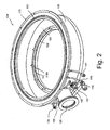
- FIG. 2 is a perspective view of an alternative embodiment having a base-plate useful in the thermal processing apparatus shown in FIG. 1;
- FIG. 3 is a cross-sectional view of a portion of a thermal processing apparatus having a pedestal heater and a thermal shield according to an embodiment of the present invention
- FIG. 4 is a diagrammatic illustration of the pedestal heater and thermal shield of FIG. 3 according to an embodiment of the present invention.
- FIG. 5 is a diagrammatic illustration of an embodiment of the thermal shield having a top layer of material with a high absorptivity and a lower layer of material with a high reflectivity according to present invention
- FIG. 6 is a diagrammatic illustration of another embodiment of the thermal shield having a cooling channel according to present invention.
- FIG. 7 is a perspective view of an embodiment of a thermal shield and an actuator according to present invention.
- FIG. 8 is a cross-sectional view of a portion of a thermal processing apparatus having a shutter according to an embodiment of the present invention.
- FIG. 9 is a cross-sectional view of a process chamber having a pedestal heater and a magnetically coupled/ferrofluidic coupled wafer rotation system according to an embodiment of the present invention.
- FIG. 10 is a cross-sectional view of a thermal processing apparatus having an across-flow injector system according to an embodiment of the present invention.
- FIG. 11 is a cross-sectional side view of a portion of the thermal processing apparatus of FIG. 10 along angle ⁇ of FIG. 13 showing positions of injector orifices in relation to the liner and of exhaust slots in relation to the wafers according to an embodiment of the present invention
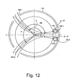
- FIG. 12 is a plan view of a portion of the thermal processing apparatus of FIG. 10 taken along the line A-A of FIG. 10 showing gas flow from orifices of a primary injector at an angle ⁇ of 0 degrees and a secondary injector at an angle ⁇ of 180 degrees relative to the substrate center across a wafer and to an exhaust port according to an embodiment of the present invention;
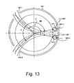
- FIG. 13 is a plan view of a portion of the thermal processing apparatus of FIG. 10 taken along the line A-A of FIG. 10 showing gas flow from orifices of a primary injector at an angle ⁇ of 180 degrees and a secondary injector at an angle ⁇ of 180 degrees relative to the substrate center across a wafer and to an exhaust port;
- FIG. 14 is a plan view of a portion of the thermal processing apparatus of FIG. 10 taken along the line A-A of FIG. 10 showing gas flow from orifices of a primary injector at an angle ⁇ of 75 degrees and a secondary injector at an angle ⁇ of 75 degrees relative to the substrate center across a wafer and to an exhaust port;
- FIG. 15 is a plan view of a portion of the thermal processing apparatus of FIG. 10 taken along the line A-A of FIG. 10 showing gas flow from orifices of a primary injector at an angle ⁇ of 0 degrees and a secondary injector at an angle ⁇ of 0 degrees relative to the substrate center across a wafer and to an exhaust port;
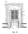
- FIG. 16 is a cross-sectional view of a thermal processing apparatus having an alternative up-flow injector system according to an embodiment of the present invention.
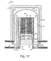
- FIG. 17 is a cross-sectional view of a thermal processing apparatus having an alternative down-flow injector system according to an embodiment of the present invention.
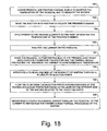
- FIG. 18 is flowchart showing an embodiment of a process for thermally processing a batch of wafers according to an embodiment of the present invention whereby each wafer of the batch of wafers is quickly and uniformly heated to the desired temperature;
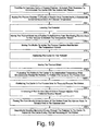
- FIG. 19 is flowchart showing another embodiment of a process for thermally processing a batch of wafers according to an embodiment of the present invention whereby each wafer of the batch of wafers is quickly and uniformly heated to the desired temperature;
- FIG. 20 is a cross-sectional view of a thermal processing apparatus including an across-flow liner according to one embodiment of the present invention.
- FIG. 21 is a perspective external view of an across-flow stepped liner showing a longitudinal bulging section according to one embodiment of the present invention.
- FIG. 22 is a perspective external view of an across-flow stepped liner reverse that of FIG. 21 showing a plurality of exhaust slots in the liner according to one embodiment of the present invention
- FIG. 23 is a side view of an across-flow liner in accordance with one embodiment of the present invention.
- FIG. 24 is a top plan view of an across-flow liner in accordance with one embodiment of the present invention.
- FIG. 25 is a partial top plan view of an across-flow liner in accordance with one embodiment of the present invention.
- FIG. 26 is a perspective inverted view of one embodiment of an across-flow injection system
- FIG. 27 is a perspective inverted view of another embodiment of an across-flow injection system.
- FIG. 28 is a plan view of an across-flow liner with a bulging section showing gas flow from orifices of a first injector at an angle ⁇ of 180 degrees and orifices of a second injector at an angle ⁇ of 180 degrees relative to a substrate center that impinges the liner inner wall prior to flowing across a wafer and exiting an exhaust slot in opposition to the bulging section;
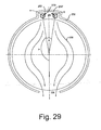
- FIG. 29 is a plan view of an across-flow liner with a bulging section showing gas flow from orifices of a first injector at an angle ⁇ of 110 degrees and orifices of a second injector at an angle P of 110 degrees relative to a substrate center that impinges each other prior to flowing across a wafer and exiting an exhaust slot in opposition to the bulging section;
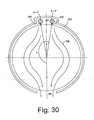
- FIG. 30 is a plan view of an across-flow liner with a bulging section showing gas flow from orifices of a first injector at an angle ⁇ of 0 degrees and orifices of a second injector at an angle ⁇ of 0 degrees relative to a substrate center directing to the center of a wafer and exiting an exhaust slot in opposition to the bulging section;
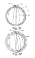
- FIGS. 31 and 32 are particle trace graphical representations showing gas flow lines across the surface of a wafer inside a chamber including an across-flow liner having a bulging section (FIG. 31) and a circular cross section (FIG. 32) and two injectors each having injection orifices defining an angle relative to the wafer center of 180 degrees where the flow from the orifice of the left injector is ten times that of the right injector and identical flows in FIGS. 31 and 32;
- FIGS. 33 and 34 are particle trace graphical representations showing gas flow lines across the surface of a wafer inside a chamber including an across-flow liner having a bulging section (FIG. 33) and a circular cross section (FIG. 34) and two injectors each having injection orifices defining an angle relative to the wafer center of 75 degrees where the flow from the orifice of the left injector is ten times that of the right injector and identical flows in FIGS. 33 and 34;
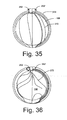
- FIGS. 35 and 36 are particle trace graphical representations showing gas flow lines across the surface of a wafer inside a chamber including an across-flow liner having a bulging section (FIG. 35) and a circular cross section (FIG. 36) and two injectors each having injection orifices defining an angle relative to the wafer center of 0 degrees where the flow from the orifice of the left injector is ten times that of the right injector and identical flows in FIGS. 35 and 36;
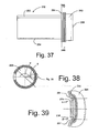
- FIG. 37 is a side view of the across-flow liner shown in cross section in FIGS. 28-31, 33 and 35;
- FIG. 38 is a cross-sectional view of the across-flow liner of FIG. 37 along line 38A-38B showing a heat shield in accordance with one embodiment of the present invention where angle ⁇ defines the center of the exhaust slot above the depicted view;
- FIG. 39 is a magnified cross-sectional inset view of the circled portion of FIG. 38;
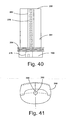
- FIG. 40 is a partially transparent side view showing an elongated injector forming an h-tube in an across-flow liner having a bulging section;
- FIG. 41 is a magnified cross-sectional view of the notched injector engagement opening in the open end of the liner shown in FIG. 40;
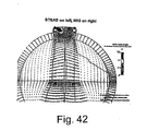
- FIG. 42 is a computational fluid dynamics (CFD) demonstration for a thermal processing apparatus including an across-flow liner and an injection system as shown in FIG. 28 flowing bis tertbutylamino silane (BTBAS) from the left injector and ammonia from the right injector;
- CFD computational fluid dynamics
- FIG. 43 is CFD demonstration for a thermal processing apparatus including an across-flow liner and an injection system as shown in FIG. 29 flowing from BTBAS and ammonia from the right and left injectors, respectively;
- FIG. 44 is CFD demonstration for a thermal processing apparatus including an across-flow liner and an injection system as shown in FIG. 30 flowing BTBAS and ammonia from the right and left injectors, respectively;
- FIG. 45 is an exploded view of the interface between various sized vertical injectors and base-plates of an inventive thermal processing system
- FIG. 46 is a perspective semitransparent view of an inventive liner
- FIG. 47 is a cross-sectional view of the inventive liner depicted in FIG. 46;
- FIG. 48 is a schematic depicting trace lines derived from computational fluid dynamic studies and showing a wafer zone of high reactivity for a thermal processing system employing the liner of FIG. 46;
- FIG. 49 is a schematic depicting trace lines derived from computational fluid dynamic studies and showing a wafer zone of high reactivity for a thermal processing system employing the liner of FIG. 36;
- FIG. 50 is a perspective semitransparent cutaway view of an inventive liner having a bulging section accommodating each of the injectors;
- FIG. 51 is a cross-sectional view of the inventive liner depicted in FIG. 50;
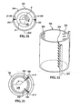
- FIG. 52 is a perspective semitransparent cutaway view of an inventive liner.
- FIG. 53 is a cross-sectional view of the inventive liner depicted in FIG. 52.
- the present invention is directed to an apparatus and method for processing a relatively small number or mini-batch of one or more work pieces, such as semiconductor substrates or wafers, held in a carrier, such as a cassette or boat, that provides reduced processing cycle times and improved process uniformity.
- a carrier such as a cassette or boat
- the present invention is directed to an apparatus and method for processing a large number or large batch of one or more work pieces, and provides reduced processing cycle times and improved process uniformity.
- thermal processing it is meant processes in which the work piece or wafer is heated to a desired temperature which is typically in the range of about 350°C to 1300°C, and can include temperatures as low as 75°C.
- thermal processing of semiconductor wafers can include heat treating, annealing, diffusion or driving of dopant material into the wafer substrates, deposition or growth of layers of material on the wafer surface via, for example, chemical vapor deposition (CVD) and etching or removal of material from the wafer substrates.
- CVD chemical vapor deposition
- thermal processing apparatus A thermal processing apparatus according to an embodiment will now be described with reference to FIG. 1. For purposes of clarity, many of the details of thermal processing apparatuses that are widely known and are widely known to a person of skill in the art have been omitted. Such detail is described in more detail in, for example, commonly assigned U.S. Patent No. 4,770,590 , which is incorporated herein by reference.
- FIG. 1 is a cross-sectional view of an embodiment of a thermal processing apparatus for thermally processing a batch of semiconductor wafers.
- the thermal processing apparatus 100 generally includes a vessel 101 that encloses a volume to form a process chamber 102 having a support 104 adapted for receiving a carrier or boat 106 with a batch of wafers 108 held therein, and heat source or furnace 110 having a number of heating elements 112-1, 112-2 and 112-3 (referred to collectively hereinafter as heating elements 112) for raising a temperature of the wafers to the desired temperature for thermal processing.
- the thermal processing apparatus 100 further includes one or more optical or electrical temperature sensing elements, such as a resistance temperature device (RTD) or thermocouple (T/C), for monitoring the temperature within the process chamber 102 and controlling operation of the heating elements 112.
- the temperature sensing element is a profile T/C 114 that has multiple independent temperature sensing nodes or points (not shown) for detecting the temperature at multiple locations within the process chamber 102.
- the thermal processing apparatus 100 also includes one or more injectors 116 (only one of which is shown) for introducing a fluid, such as a gas or vapor, into the process chamber 102 for processing or cooling the wafers 108, and one or more purge ports or vents 118 (only one of which is shown) for introducing a gas to purge the process chamber and cool the wafers.
- a liner 120 increases the concentration of processing gas or vapor near the wafers 108 in a process zone 128 in which the wafers are processed, and reduces contamination of the wafers from flaking or peeling of deposits that can form on interior surfaces of the process chamber 102. Processing gas or vapor exits the process zone through exhaust ports or slots 121 in the chamber liner 120.
- the vessel 101 is sealed by a seal, such as an o-ring 122, to a platform or base-plate 124 to form the process chamber 102, which completely encloses the wafers 108 during thermal processing.
- the dimensions of the process chamber 102 and the base-plate 124 are selected to provide a rapid evacuation, rapid heating and a rapid backfilling of the process chamber.
- the vessel 101 and the base-plate 124 are sized to provide a process chamber 102 having dimensions selected to enclose a volume substantially no larger than necessary to accommodate the liner 120 with the carrier 106 and wafers 108 held therein.
- the vessel 101 and the base-plate 124 are sized to provide a process chamber 102 having dimensions of from about 125 to about 150% of that necessary to accommodate the liner 120 with the carrier 106 and wafers 108 held therein, and more preferably, the process chamber has dimensions no larger than about 125% of that necessary to accommodate the liner 120 and the carrier 106 and wafers 108 in order to minimize the chamber volume and thereby reduce pump down and back-fill time required.
- Openings for the injectors 116, T/Cs 114 and vents 118 are sealed using seals such as o-rings, VCR®, or CF® fittings.
- Gases or vapor released or introduced during processing are evacuated through a foreline or exhaust port 126 formed in a wall of the process chamber 102 (not shown) or in a plenum 127 of the base-plate 124, as shown in FIG. 1.
- the process chamber 102 can be maintained at atmospheric pressure during thermal processing or evacuated to a vacuum as low as 5 millitorr through a pumping system (not shown) including one or more roughing pumps, blowers, hi-vacuum pumps, and roughing, throttle and foreline valves. In the alternative, the process chamber can be evacuated to a vacuum lower than 5 millitorr.
- the base-plate 124 further includes a substantially annular flow channel 129 adapted to receive and support an injector 116 including a ring 131 from which depend a number of vertical injector tube or injectors 116A.
- the injectors 116A can be sized and shaped to provide an up-flow, down-flow or across-flow flow pattern, as described below.
- the ring 131 and injectors 116A are located so as to inject the gas into the process chamber 102 between the boat 106 and the vessel 101.
- the injectors 116A are spaced apart around the ring 131 to uniformly introduce process gas or vapor into the process chamber 102, and may, if desired, be used during purging or backfilling to introduce a purge gas into the process chamber.
- the base-plate 124 is sized in a short cylindrical form with an outwardly extending upper flange 133, a sidewall 135, and an inwardly extending base 137.
- the upper flange 133 is adapted to receive and support the vessel 101, and contains an o-ring 122 to seal the vessel to the upper flange.
- the base 137 is adapted to receive and support the liner 120 between the ring 131 of injectors 116 and the sidewall 135.
- the base-plate 124 shown in FIG. 2 incorporates various ports including backfill or purge gas inlet ports 139 and 143, cooling ports 145 and 147 which provide cooling fluid to the base-plate 124, and a pressure monitoring port 149 for monitoring pressure within the process chamber 102.
- Process gas inlet ports 151 and 161 introduce a gas from a gas supply (not shown) to the injectors 116A.
- the backfill or purge ports 139 and 143 are provided at the sidewall 135 of the base-plate 124 principally to introduce a gas from a vent or purge gas-supply (not shown) to the vents 118.
- a mass flow controller (not shown) or any other suitable flow controller is placed in line between the gas supplies and the ports 139, 143, 151 and 161 to control the gas flow into the process chamber 102.
- the vessel 101 and liner 120 can be made of any metal, ceramic, crystalline or glass material that is capable of withstanding the thermal and mechanical stresses of high temperature and high vacuum operation, and which is resistant to erosion from gases and vapors used or released during processing.
- the vessel 101 and liner 120 are made from an opaque, translucent or transparent quartz glass having a sufficient thickness to withstand the mechanical stresses of the thermal processing operation and resist deposition of process byproducts. By resisting deposition of process byproducts, the vessel 101 and liner 120 reduce the potential for contamination of the processing environment. More preferably, the vessel 101 and liner 120 are made from quartz that reduces or eliminates the conduction of heat away from the process zone 128 in which the wafers 108 are processed.
- the batch of wafers 108 is introduced into the thermal processing apparatus 100 through a load lock or loadport (not shown) and then into the process chamber 102 through an access or opening in the process chamber or base-plate 124 capable of forming a gas tight seal therewith.
- the process chamber 102 is a vertical reactor and the access utilizes a movable pedestal 130 that is raised during processing to seal with a seal, such as an o-ring 132 on the base-plate 124, and lowered to enable an operator or an automated handling system, such as a boat handling unit (BHU) (not shown), to position the carrier or boat 106 on the support 104 affixed to the pedestal.
- a boat handling unit BHU
- the heating elements 112 include elements positioned proximal to a top 134 (elements 112-3), side 136 (elements 112-2) and bottom 138 (elements 112-1) of the process chamber 102. In the alternative, heating elements 112 do not include elements positioned proximal to the bottom 138 of the process chamber 102.
- the heating elements 112 surround the wafers to achieve a good view factor of the wafers and thereby provide an isothermal process zone 128 in the process chamber in which the wafers 108 are processed.
- the heating elements 112-1 proximal to the bottom 138 of the process chamber 102 can be disposed in or on the pedestal 130. If desired, additional heating elements may be disposed in or on the base plate 124 to supplement heat from the heating elements 112-1.
- the heating elements 112-1 proximal to the bottom of the process chamber 102 preferably are recessed in the movable pedestal 130.
- the pedestal 130 is made from a thermally and electrically insulating material or insulating block 140 having electric, resistive heating elements 112-1 embedded therein or affixed thereto.
- the pedestal 130 further includes one or more T/Cs 141 used to control the heating elements 112-1. In the configuration shown, the T/Cs 141 are embedded in the center of the insulating block 140.
- the side heating elements 112-2 and the top heating elements 112-3 may be disposed in or on an insulating block 110 about the vessel 101.
- the heating elements 112-1 proximal to the bottom 138 of the process chamber 102 have a maximum power output of from about 0.1 kW to about 10 kW with a maximum process temperature of at least 1150°C. More preferably, these bottom heating elements 112-1 have a power output of at least about 3.8 kW with a maximum process temperature of at least 950°C.
- the side heating elements 112-2 are functionally divided into multiple zones, each of which are capable of being operated independently at different power levels and duty cycles from each other. The heating elements 112 are controlled in any suitable manner.
- Contamination from the insulating block 140 and bottom heating elements 112-1 is reduced if not eliminated by housing the heating element and insulation block in an inverted quartz crucible 142, which serves as a barrier between the heating element and insulation block and the process chamber 102.
- the crucible 142 is also sealed against any external environment to further reduce or eliminate contamination of the processing environment.
- the interior of the crucible 142 is at standard atmospheric pressure and should be strong enough to withstand a pressure differential of as much as 1 atmosphere.
- the bottom heating elements 112-1 are powered to maintain an idle temperature lower than the desired processing temperature.
- the idle temperature can be from 50-150°C.
- the idle temperature can be set higher for certain processes, such as those having a higher desired processing temperature or higher desired ramp-up rate.
- a higher idle temperature can be employed to reduce thermal cycling effects on the bottom heating elements 112-1, thereby extending element life.
- the bottom heating elements 112-1 can be ramped to or held at an elevated preprocess temperature during the push or load, that is while the pedestal 130 with a boat 106 of wafers 108 positioned thereon is being raised.
- the bottom heating elements 112-1 reach the desired process temperature at the same time as the heating elements 112-2 and 112-3 located proximal to the top 136 and side 134 respectively, of the process chamber 102.
- ramping up of bottom heating elements 112-1 can be initiated before the pedestal 130 is raised, for example while the last of the wafers 108 in a batch are being loaded.
- a purge line for air or an inert purge gas such as nitrogen
- nitrogen is injected through a passage 144 through the center of the insulating block 140 and allowed to flow out between the top of the insulating block 140 and the interior of the crucible 142 to a perimeter thereof.
- the hot nitrogen is then exhausted to the environment either through High Efficiency Particulate Air (HEPA) filter (not shown) or to a facility exhaust (not shown).
- HEPA High Efficiency Particulate Air
- This center injection configuration facilitates the faster cooling of the center of the wafers 108, and therefore is ideal to minimize the center/edge temperature differential of the bottom wafer or wafers.
- the idle temperature can be set higher and thus closer to the desired processing temperature and thereby reduce the effects of thermal cycling.
- the resistive heating elements are formed from an aluminum containing alloy, such as Kanthal®
- baking out the heating elements 112-1 in an oxygen rich environment promotes an aluminum oxide surface growth.
- the insulating block 140 can further include an oxygen line (not shown) to promote the formation of the protective oxide surface coat during bake out of the heating elements 112-1.
- oxygen for bake out can be introduced through the passage 144 used during processing to supply cooling nitrogen via a three-way valve.
- FIG. 3 is a cross-sectional view of a portion of a thermal processing apparatus 100.
- FIG. 3 shows the thermal processing apparatus 100 while the wafers 108 are being loaded or unloaded while the pedestal 130 is in the lowered position.
- the thermal processing apparatus 100 further includes a thermal shield 146 that can be rotated or slid into place between the pedestal 130 and the lower wafer 108 in the boat 106.
- the thermal shield is reflective on the side facing the heating elements 112-1 and absorptive on the side facing the wafers 108.
- Purposes of the thermal shield 146 include increasing the rate of cooling of the wafers 108, and assisting in maintaining the idle temperature of the pedestal 130, thereby decreasing the time required to ramp up the process chamber 102 to a desired processing temperature.
- An embodiment of a thermal processing apparatus having a thermal shield will now be described in further detail with reference to FIGS. 3 through 6.
- the thermal shield 146 is attached via an arm 148 to a rotable shaft 150.
- Rotable shaft 150 is turned by an electric, pneumatic or hydraulic actuator and allows thermal shield 146 to be rotated into a first position between the pedestal 130 and the wafers 108 in the boat 106 during the pull or unload cycle, and rotated to a second position not between the pedestal 130 and the wafers 108.
- the rotable shaft 150 is mounted on or affixed to the mechanism (not shown) used for raising and lowering the pedestal 130, thereby enabling the thermal shield 146 to be rotated into position as soon as the top of the pedestal has cleared the process chamber 102.
- the shield 146 in place during a load cycle enables the heating elements 112-1 to be heated to a desired temperature more rapidly than would otherwise be possible. Similarly, during an unload cycle the shield 146 helps in cooling the wafers 108, particularly those closer to the pedestal 130, by reflecting the heat radiating from the pedestal heating elements 112-1.
- the rotable shaft 150 can be mounted on or affixed to another part of the thermal processing apparatus 100 and adapted to move axially in synchronization with the pedestal 130, or to rotate the thermal shield 146 into position only when the pedestal is fully lowered.
- FIG. 4 is a diagrammatic illustration of the pedestal heating elements 112-1 and thermal shield 146 of FIG. 3 illustrating the reflection of thermal energy or heat radiating from the bottom heating elements back to the pedestal 130 and the absorption of thermal energy or heat radiating from the lower wafer 108 in the batch of wafers. It has been determined that the desired characteristics, high reflectivity and high absorptivity, can be obtained using a number of different materials, such as metals, ceramic, glass or polymeric coatings, either individually or in combination. By way of example the following table lists various suitable materials and corresponding parameters. Table I Material Absorptivity Reflectivity Stainless Steel 0.2 0.8 Opaque Quartz 0.5 0.5 Polished Aluminum 0.03 0.97 Silicon Carbide 0.9 0.1
- the thermal shield 146 can be made from a single material such as silicon-carbide (SiC), opaque quartz or stainless steel which has been polished on one side and scuffed, abraded or roughened on the other. Roughening a surface of the thermal shield 146 can significantly change its heat transfer properties, particularly its reflectivity.
- SiC silicon-carbide
- opaque quartz or stainless steel which has been polished on one side and scuffed, abraded or roughened on the other. Roughening a surface of the thermal shield 146 can significantly change its heat transfer properties, particularly its reflectivity.
- the thermal shield 146 can be made from two different layers of material.
- FIG. 5 is a diagrammatic illustration of a thermal shield 146 having a top layer 152 of material (with a high absorptivity), such as SiC or opaque quartz, and a lower layer 154 of material (with a high reflectivity), such as polished stainless steel or polished aluminum.
- a top layer 152 of material with a high absorptivity
- a lower layer 154 of material with a high reflectivity
- polished stainless steel or polished aluminum such as polished stainless steel or polished aluminum.
- the lower layer 154 can be an extremely thin layer or film of polished metal deposited, formed or plated on a quartz plate that forms the top layer 152.
- the materials can be integrally formed or interlocking, or joined by conventional means such as bonding or fasteners.
- FIG. 6 shows the thermal shield 146 with an internal cooling channel 156 to further insulate the wafers 108 from the bottom heating elements 112-1.
- the cooling channel 156 is formed between two different layers of material.
- the cooling channel 156 can be formed by milling or any other suitable technique in a highly absorptive opaque quartz layer 152, and be covered by a metal layer 154.
- the cooling channel 156 can be formed in the metal layer 154 or both the metal layer and the quartz layer 152.
- FIG. 7 is a perspective view of an embodiment of a thermal shield assembly 153 including the thermal shield 146, arm 148, rotable shaft 150 and an actuator 155.
- the thermal processing apparatus 100 can further include a shutter 158 that can be rotated, slid or otherwise moved into place above the boat 106 to isolate the process chamber 102 from the outside or load port environment when the pedestal 130 is in the fully lowered position.
- the shutter 158 can be slid into place above the carrier 106 when the pedestal 130 is in a lowered position, and raised to isolate the process chamber 102.
- the shutter 158 can be rotated or swung into place above the carrier 106 when the pedestal 130 is in a lowered position, and subsequently raised to isolate the process chamber 102.
- the shutter 158 may be rotated about or relative to threaded screw or rod to simultaneously raise the shutter to isolate the process chamber 102 as it is swung into place above the carrier 106.
- the shutter 158 could form a vacuum seal against the base-plate 124 to allow the process chamber 102 to be pumped down to the process pressure or vacuum. For example, it may be desirable to pump down the process chamber 102 between sequential batches of wafers to reduce or eliminate the potential for contaminating the process environment.
- Forming a vacuum seal is preferably done with a large diameter seal, such as an o-ring, and thus the shutter 158 can desirably include a number of water channels 160 to cool the seal.
- the shutter 158 seals with the same o-ring 132 used to seal with the crucible 142 when the pedestal 130 is in the raised position.
- the shutter 158 is simply an insulating device used to reduce heat loss from the bottom of the process chamber.
- One embodiment for accomplishing this involves the use of an opaque quartz plate, which mayor may not further include a number of cooling channels underneath or internal thereto.
- the shutter 158 is moved into position below the process chamber 102 and then raised to isolate the process chamber by one or more electric, hydraulic or pneumatic motors (not shown).
- the motor is a pneumatic motor using from about 15 to 60 pounds per square inch gauge (PSIG) air, which is commonly available on the thermal processing apparatus 100 for operation of pneumatic valves.
- the shutter 158 can comprise a plate having a number of wheels attached via short arms or cantilevers to two sides thereof (not shown). In operation, the plate or shutter 158 is rolled into position beneath the process chamber 102 on two parallel guide rails (not shown). Stops on the guide rails then cause the cantilevers to pivot translating the motion of the shutter 158 into an upward direction to seal the process chamber 102.
- PSIG pounds per square inch gauge
- the thermal processing apparatus 100 further includes a magnetically coupled wafer rotation system 162 that rotates the support 104 and the boat 106 along with the wafers 108 supported thereon during processing.
- the thermal apparatus 100 uses a rotational ferrofluidics seal (not shown) to rotate the support 104 and the boat 106 along with the wafers 108 supported thereon during processing.
- Rotating the wafers 108 during processing improves within wafer (WIW) uniformity by averaging out any non-uniformities in temperature and process gas flow to create a uniform wafer temperature and species reaction profile.
- the wafer rotation system 162 is capable of rotating the wafers 108 at a speed of from about 0.1 to about 10 revolutions per minute (RPM).
- the wafer rotation system 162 includes a drive assembly or rotating mechanism 164 having a rotating motor 166, such as an electric or pneumatic motor, and a magnet 168 encased in a chemically resistive container, such as annealed polytetrafluoroethylene or stainless steel.
- a chemically resistive container such as annealed polytetrafluoroethylene or stainless steel.
- a steel ring 170 located just below the insulating block 140 of the pedestal 130, and a drive shaft 172 with the insulating block transfer the rotational energy to another magnet 174 located above the insulating block in a top portion of the pedestal.
- the steel ring 170, drive shaft 172 and second magnet 174 are also encased in a chemically resistive container compound.
- the magnet 174 located inside of the pedestal 130 magnetically couples through the crucible 142 with a steel ring or magnet 176 embedded in or affixed to the support 104 in the process-chamber 102.
- a ferrofluidic coupling is provided between the rotating mechanism 164 and the pedestal 130.
- the wafer rotation system 162 can further include one or more sensors (not shown) to ensure proper boat 106 position and proper magnetic coupling between the steel ring or magnet 176 in the process chamber 102 and the magnet 174 in the pedestal 130.
- a boat position verification sensor which determines the relative position of the boat 106 is particularly useful.
- the boat position verification sensor includes a sensor protrusion (not shown) on the boat 106 and an optical or laser sensor located below the base-plate 124. In operation, after the wafers 108 have been processed the pedestal 130 is lowered about 3 inches below the base-plate 124. There, the wafer rotation system 162 is commanded to turn the boat 106 until the boat sensor protrusion can be seen. Then, the wafer rotation system 162 is operated to align the boat so that the wafers 108 can be unloaded. After this is done, the boat is lowered to the load/unload height.
- inventive injectors collectively 215 are preferably used in the thermal processing apparatus 100-2.
- the injectors 215, of which two are depicted, are distributive or across-flow injectors 215-1 and 215-2 that process gas or vapor introduced through injector orifices 180 on one side of the wafers 108 held in boat 106 and caused to flow across the surfaces of the wafers 108 in a laminar flow to exhaust ports or slots 182 in liner 181.
- the exhaust ports or slots 182 are depicted as two courses of ports or slots 182-1 and 182-2 that are positioned at angles ⁇ and ⁇ ' relative to a first injector 215-1 through the center of a wafer 108.
- the number of courses of vertically displaced exhaust ports or slots 182 is one, two, or more with each defining an angle ⁇ n where n is the number of the course of exhaust ports or slots 182-n where ⁇ angles increase in degrees with each successive course such that ⁇ ' ⁇ 2 ... ⁇ n .
- the across-flow injectors 215-1 and 215-2 improve wafer uniformity within a batch of wafers 108 by providing an improved distribution of process gas or vapor over earlier gas flow configurations.
- the injector orifices 180 are aligned with wafer support positions to promote each wafer 108 receiving a similar fluid flow across the surface regardless of wafer vertical position within the wafer batch in the inventive liner.
- across-flow injectors collectively 215 can serve purposes other than reactant fluid gas or vapor delivery, including the injection of gases (e.g., helium, nitrogen, hydrogen) for forced convective cooling between the wafers 108.
- gases e.g., helium, nitrogen, hydrogen
- the injector 215 orifices 180 are sized, shaped and positioned to provide a spray pattern that promotes forced convective cooling between the wafers 108 in a manner that does not create a large temperature gradient across the wafer.
- FIG. 11 is a cross-sectional side view of a portion of the thermal processing apparatus 100 of FIG. 10" showing illustrative portions of the injector orifices 180 in relation to the liner 181 and the exhaust ports or slots 182 in relation to the wafers 108.
- FIG. 12 is a plan view of a portion of the thermal processing apparatus 100-2 of FIG. 10 taken along the line A-A of FIG. 10 showing laminar gas flow from the orifices 180-1 and 180-2 of primary and secondary injectors 215-1, 215-2, across an illustrative one of the wafers 108 and to exhaust slots 182-1 and 182-2 according to one embodiment. It should be noted that the position of the exhaust slot 182 as shown in FIGS. 10 and 11 is shown along angle ⁇ to allow illustration of the exhaust ports or slots and injectors 215-1 in a single cross-sectional view of a thermal processing apparatus.
- the process gas or vaporfrom injector 215-1 is directed towards the wafer 108 while injector 215-2 is directed away from the wafers 108 and toward the liner 181 to promote mixing of the process gas or vapor before it reaches the wafers.
- An angle ⁇ of 0 degrees is defined through the center of injector 215-1 extending between the orifice 180-1 and the center of wafer 108.
- an angle ⁇ of 180 degrees is defined about the center of injector 215-2 between 180-2 and the wafer center.
- This configuration of orifices 180-1 and 180-2 is particularly useful for processes or recipes in which different reactants that vary significantly in molecular weight are introduced from each of the primary and secondary injectors 215-1, 215-2, for example to form a multi-component film or layer.
- FIG. 13 is a plan view of a portion of the thermal processing apparatus 100-2 of FIG. 10 taken along the line A-A of FIG. 10 showing an alternative gas flow path from the orifices 180 of the primary and secondary injector 215-1, 215-2, across an illustrative one of the wafers 108 and to the exhaust slots 182-1 and 182-2 in which the angles ⁇ and ⁇ are both 180 degrees.
- FIG. 14 is another plan view of a portion of the thermal processing apparatus 100-2 of FIG. 10 taken along the line A-A of FIG. 10 showing an alternative gas flow path from the orifices 180 of the primary and secondary injector 215-1, 215-2, across an illustrative one of the wafers 108 and to the exhaust slots 182-1 and 182-2 in which angles ⁇ and ⁇ are both 75 degrees.
- FIG. 15 is another plan view of a portion of the thermal processing apparatus 100-2 of FIG. 10 taken along the line A-A of FIG. 10 showing an alternative gas flow path from the orifices 180 of the primary and secondary injector 215-1, 215-2, across an illustrative one of the wafers 108 and to the exhaust slots 182-1 and 182-2 in which angles ⁇ and ⁇ are both 0 degrees.
- FIG. 16 is a cross-sectional view of a thermal processing apparatus 100-3 having two or more up-flow injectors 116-1 and 116-2 according to an alternative embodiment.
- process gas or vapor admitted from the process injectors 116-1 and 116-2 having respective outlet orifices low in the process chamber 102 flows up and across the wafers 108, and spent gases exit exhaust slots 182 in the top of the liner 120.
- An up-flow injector system is also shown in FIG. 1.
- FIG. 17 is a cross-sectional view of a thermal processing apparatus 100-4 having a down-flow injector system according to an alternative embodiment.
- process gas or vapor admitted from process injectors 116-1 and 116-2 having respective orifices high in the process chamber 102 flows down and across the wafers 108, and spent gases exit exhaust slots 182 in the lower portion of the liner 120'.
- the injectors 116, collectively numbered at 215, and/or the liners 120 or 181 are quickly and easily replaced or swapped with other injectors and liners having different points for the injection and exhausting of the process gas from the process zone 128.
- the embodiment of the across-flow injector 215 shown in FIG. 10 adds a degree of process flexibility by enabling the flow pattern within the process chamber 102 to be quickly and easily changed. This can be accomplished through the use of easily installable injector assemblies 215 and liners 181 to convert the flow geometry from cross-flow to an up-flow, etc., as well as adjust the across-flow fluid paths over a wafer substrate.
- a base-plate as detailed in FIG. 2 is provided with a series of apertures adapted to receive injectors so as to facilitate positional change of an injector relative to exhaust ports or slots and other injectors if present.
- a representative factor to be considered in injector position relative to other injectors is reaction rate of fluids exiting the injectors under processing conditions.
- the injector angle defined through the center of an injector between the wafer center and the center of a series of injector orifices, denoted as angle ⁇ with respect to injector 215-1 in FIGS. 12-15, is adjusted through injector rotation so as to seat an index pin with a complementary notch in the liner or base plate.
- injector orifice rotation angle is also optionally achieved with conventional tube securement techniques capable of forming a gas-tight seal such as through use of a circumferential clamp ring, , a key simultaneously engaging an injector, a liner base, and a frinction fit.
- a different diameter injector is accommodated through the enlargement of injector engagement aperture 125 to accommodate the outer diameter of the enlarged injector in instances when the injector outer diameter is greater than that of an existing aperture in the base 124 engaging an inventive liner.
- an injector tapers to a diameter adapted to engage a base aperture 125.
- the coupling 128 is optionally fused to the base of an injector or formed as a collet. Forms of accommodating different diameter injectors other than resizing an aperture are detailed with greater specificity with regard to FIG. 45.
- a number of injectors greater than one or two injectors, as depicted for visual clarity in the figures, are readily accommodated through the provision of additional apertures formed within a liner base along with the provision of additional hardware and fittings to accommodate fluid communication with the additional injector.
- An aperture in a base-plate not coupled to an injector is sealed with a plug (not shown) formed of quartz or other material suitable for the reaction process occurring within an inventive liner.
- inventive liners that vary in attributes such as the inclusion of one or more bulging sections with each bulging section accommodating one or more injectors, the number of vertical courses of exhaust ports or slots, the angular relationship between a first injector and a vertical course of exhaust ports or slots in the liner, the vertical course being composed of exhaust ports, exhaust slots, or a combination thereof; vertical height and spacing between vertically displaced exhaust ports, and the total number of injectors.
- the injectors 116, 215 and the liners 120 or 181 can be separate components, or the injector can be integrally formed with liner as a single piece. The latter embodiment is particularly useful in applications where it is desirable to frequently change the process chamber 102 configuration.
- FIG. 18 is a flowchart showing steps of a method for thermally processing a batch of wafers 108 wherein each wafer of the batch of wafers is quickly and uniformly heated to the desired temperature.
- the pedestal 130 is lowered, and the thermal shield 142 is moved into a position while the pedestal 130 is lowered to reflect heat from the bottom heating element 112-1 back to the pedestal 130 to maintain the temperature thereof, and to insulate the finished wafers 108 (step 190).
- the shutter 158 is moved into position to seal or isolate the process chamber 102 (step 92), and the power is applied to the heating elements 112-2, 112-3, to begin preheating the process chamber 102 to or maintain at an intermediate or idling temperature (step 194).
- a carrier or boat 106 loaded with new wafers 108 is positioned on the pedestal 130 (step 196).
- the pedestal 130 is raised to position the boat in the process zone 128, while simultaneously removing the shutter 158, the thermal shield 146, and ramping up the bottom heating element 112-1 to preheat the wafers to an intermediate temperature (step 197).
- the thermal shield 146 is removed just before the boat 106 is positioned in the process zone 128.
- a fluid such as a process gas or vapor, is introduced on one side of the wafers 108 through a plurality of injection ports 180 (step 198).
- the fluid flows from the injection ports 180 across surfaces of the wafers 108 to exhaust ports 182 positioned in the liner 120 on the opposite side of the wafers relative to the injection ports (step 199).
- the boat 106 can be rotated within the process zone 128 during thermal processing of the batch of wafers 108 to further enhance uniformity of the thermal processing, by magnetically coupling mechanical energy through the pedestal 130 to the carrier or boat 106 to reposition it during thermal processing of the wafers (step 200).
- FIG. 19 is a flowchart showing steps of an embodiment of a method for thermally processing a batch of wafers 108 in a carrier.
- an apparatus 100 is provided having a process chamber 102 with dimensions and a volume not substantially larger than necessary (guard heaters absent) to accommodate the carrier 106 with the wafers 108 held therein (step 202).
- the pedestal 103 is lowered, and the boat 106 with the wafers 108 held therein positioned thereon (step 202).
- the pedestal 130 is raised to insert the boat in the process chamber 102, while simultaneously preheating the wafers 108 to an intermediate temperature (step 204).
- Power is applied to the heating elements 112-1, 112-2, 112-3, each disposed proximate to at least one of the top wall 134, the side wall 136 and the bottom wall 138 of the process chamber 102 to begin heating the process chamber (step 206).
- power to at least one of the heating elements is adjusted independently to provide a substantially isothermal environment at a desired temperature in a process zone 128 in the processing chamber 102 (step 208).
- the pedestal 130 is lowered, and the thermal shield 142 is moved into position to insulate the finished wafers 108 and to reflect heat from the bottom heating element 112-1 back to the pedestal 130 to maintain the temperature thereof (step 210).
- the shutter 158 is moved into position to seal or isolate the process chamber 102, and power applied to the heating elements 112-2, 112-3, to maintain the temperature of the process chamber (step 212).
- the boat 106 is then removed from the pedestal 130 (step 214), and another boat loaded with a new batch of wafers to be processed positioned on the pedestal (step 216).
- the shutter 158 is repositioned or removed (step 218), and the thermal shield withdrawn or repositioned to preheat the wafers 108 in the boat 106 to an intermediate temperature while simultaneously raising the pedestal 130 to insert the boat into the process chamber 102 to thermally process the new batch of wafers (step 220).
- Stepped liners are typically used in traditional up-flow vertical furnaces to increase process gas velocities and diffusion control. They are also used as an aid to improve within-wafer uniformity.
- stepped liners do not correct down- the-stack-depletion problems, which occur due to single injection point of reactant gases forcing all injected gases to flow past all surfaces down the stack.
- the down-the-stack-depletion problem is solved.
- a flow path of least resistance may be created in the gap region between the wafer carrier and the liner inner wall instead of between the wafers. This least resistance path may cause vortices or stagnation which are detrimental to manufacturing processes. Vortices and stagnation in a furnace may create across wafer non-uniformity problems for some process chemistries.
- the present invention provides an across-flow liner that significantly improves the within-wafer uniformity by providing uniform gas flow across the surface of each substrate supported in a carrier.
- the across-flow liner of the present invention includes a longitudinal bulging section to accommodate an across-flow injection system so that the liner can be patterned and sized to conform to the wafer carrier.
- the gap between the liner and the wafer carrier is significantly reduced, and as a result, vortices and stagnation as occurred in prior art furnaces can be reduced or avoided.
- FIG. 20 shows a thermal processing apparatus 100-6 where like reference numerals correspond to those used with respect to the preceding figures and includes an across-flow liner 232 according to one embodiment of the present invention.
- the apparatus 100-6 includes a vessel 101 that forms a process chamber 102 having a support 104 adapted for receiving a wafer boat or carrier 106 with a batch of wafers 108 held therein.
- the apparatus 100-6 includes a heat source or furnace 110 that heats the wafers 108 to the desired temperature for thermal processing.
- An across-flow liner 232 is provided to increase the concentration of processing gas or vapor near wafers 108 and reduce contamination of wafers 108 from flaking or peeling of deposits that can form on interior surfaces of the vessel 101.
- the liner 232 is patterned to conform to the contour of the wafer carrier 106 and sized to reduce the gap between the wafer carrier 106 and the liner wall 233 through the inclusion of a bulging section 262 adapted to accommodate one or more injectors 215. Multiple such bulging sections optionally are provided, each accommodating one or more injectors 215 or 251.
- Such a multiple bulging section liner is depicted in FIGS. 37-39 where FIG. 38 is a cross-sectional view along line 38A-38B of FIG. 37 and FIG. 39 is an expanded view of the bulging section region base with a movable pedestal 130.
- the liner 232 is mounted to a base plate 124 and forms a seal with a movable pedestal 130.
- an across-flow injection system 250 is disposed within the long-bulging section 262 of the liner 232.
- the injection system 250 includes at least one injector 215-1 or 251. It is appreciated that in instances when multiple injectors are present, the inner diameter of each injector is independently selected. Gases are introduced into the liner volume through a plurality of injection orifices 181 or 252 from one side of the wafers 108 and carrier 106 and flow across the surface of the wafers in a laminar flow as described below.
- the orifices 181 or 252 are aligned with the wafers 108 in the support positions of the carrier 106 so as to promote vertical wafer-to-wafer (WTW) gas flow uniformity and as a result WTW processing uniformity.
- WTW wafer-to-wafer
- the area and shape of a given orifice 181 or 252 are independent of those of adjacent orifices with a given injector 215-1 or 251.
- a vertical course of a plurality of exhaust ports or slots 254 are formed in the liner 232 in a location approximately 180 degrees from the long-bulging section 262 and correspond to an angle ⁇ of 170 degrees.
- the size and pattern of the ports or slots 254 are predetermined and preferably cooperate with the spacing between and number of the injection orifices 181 or 252 to facilitate across-flow. It is appreciated that a second, third, or more vertical courses of exhaust ports or slots are cut into a liner wall 233 in a position other than the bulging section 262. While FIGS. 20-22 depict the vertical course of exhaust ports or slots 254 as uniform area rectilinear slots aligned with orifices and wafer substrates, the area and shape of an individual port or slot is independent of that of other ports or slots within the same course.
- a liner 232 is readily formed having a vertical course of exhaust ports or slots 254 and a second course of exhaust ports or slots that are rectilinear slots of a different total area or shape such as circular, oval, parallelogram, or other geometric forms, as compared to the vertical course 254.
- Such variants in liner design are provided in FIGS. 36, 50, and 52.
- the across-flow liner can be made of any metal, ceramic, crystalline or glass material that is capable of withstanding the thermal and mechanical stresses of high temperature and high vacuum operation, and which is resistant to erosion from gases and vapors used or released during processing.
- the across-flow liner is made from an opaque, translucent or transparent quartz glass.
- the liner is made from quartz that reduces or eliminates the conduction of heat away from the region or process zone in which the wafers are processed.
- the across-flow liner 232 includes a cylinder 256 having a closed end 258 and an open end 260.
- the cylinder 256 is provided with the longitudinal bulging section 262 to accommodate an across-flow injection system 250 inclusive of one or more injectors 215-1 or 251.
- the bulging section 262 extends the substantial length of the cylinder 256.
- the across-flow liner 232 is sized and patterned to conform to the contour of the wafer carrier 106 and the carrier support 104.
- the liner 232 has a first section 261 sized to conform to the wafer carrier 106 and a second section 263 sized to conform to the carrier support 104.
- the diameter of the first section 261 may differ from the diameter of the second section 263, i.e., the liner 232 may be "stepped" to conform to the wafer carrier 106 and carrier support 108 respectively.
- the first section 261 of the liner 232 has an inner diameter that constitutes about 104 to 110% of the wafer carrier 106 outer diameter.
- the second section 263 of the liner 232 has an inner diameter that constitutes about 115 to 120% of the outer diameter of the carrier support 108.
- the second section 263 may be provided with one or more heat shields 264 to protect seals such as o-rings from being overheated by heating elements.
- FIG. 23 is a side view of the across-flow liner 232.
- the longitudinal bulging section 262 extends the length of the first section 261.
- the injection system 250 is accommodated in the bulging section 262 and introduces one or more gases into the across-flow liner 232 between the wafers 108 spaced along the height of a carrier 106.
- One or more heat shields 264 is optionally provided in the second section 263.
- FIG. 24 is a cross-sectional view of the across-flow liner 232 showing the open end 263 of the cylinder 256 surrounding openings 266 in a base plate 124 for receiving the across-flow injection system 250.
- the injection system 250 has at least one injection tube 215-1 or 251 (described in detail below) to fit within the openings 266.
- the openings 266 in the base plate 124 have notches 268 for orienting and stabilizing an across-flow injection system.
- notches 268A, 268b, 268C are shown in the openings 266 for illustrative purpose, it should be noted that any number of notches can be formed so that the injection tube can be oriented to any direction up to and including 360 degrees relative to the across-flow liner 232 and to each other.
- other techniques for securing an injector in a selected rotational angle ⁇ relative to the wafer center illustratively include a circumferential clamping ring, a key simultaneously engaging an injector and a liner base, and a friction fit.
- the across-flow injection system 250 comprises one or more elongated tubes 215-1 or 251 rotatable about an axis perpendicular to the desired processing surfaces of the wafers.
- PCT/US04/031063 describes one embodiment of an injection system, the disclosure of which is hereby incorporated by reference in its entirety.
- the elongated tubes 251 are provided with a plurality of injection orifices 252 longitudinally distributed along the length of the tubes for directing reactant and other gases across the surface of each substrate.
- the injection orifices 252 have the same area and shape as the adjacent orifices.
- a second injector 252' is shown having the same inner diameter as injector 252 with like orifices 252.
- Each injector 251 and 251' is independently rotatable about the injector long axis.
- the orifices 252 of injector 251 and the orifice 252' of injector 251' are aligned to coincide with a wafer placed on a carrier so as to facilitate WTW uniformity while batch processing.
- the diameter of injectors 251 and 251' are different.
- varied diameter injectors 251 and 251' are particularly advantageous is where two gases are desired to be provided in an across-flow path over a wafer surface at similar injector pressures although at different delivery volumes.
- the area and shape of the orifices 252 and 252' are optionally varied along the injector length. It has been discovered that the vertical decrease in injector emission pressure is compensated for by increasing the area of orifices upward along the length of the injector (FIGS. 26 and 27 are inverted perspective views).
- circular orifices are optionally formed in a shape illustratively including rectilinear, oval, or combinations thereof.
- the orifices are in alignment with a wafer substrate to provide across-flow.
- the elongated injector 251 includes an index pin 253 for locking the elongated tube in one of the notches 268 in the openings 266, and the injection ports or orifices 252 are formed in line with the index pin. Therefore, when the elongated tube is installed, the index pin can be locked in one of the notches 268 and the injection ports 252 are oriented in a direction as indicated by the appropriate notch 268.
- An indicator located on the opposite end of tubes 251 further allows a user to adjust the location of the injection ports 252. This adjustment is performed before, during and after a thermal processing run without removal of the across-flow liner 232 from the vessel.
- the bulging section 262 of the across-flow liner 232 accommodates the across-flow injection system 250 therein and the liner 232 is made conformal to the contour of the wafer carrier. This confirming of the liner 232 to the wafer carrier reduces the gap between the liner and the wafer carrier, thereby reducing the vortices and stagnation in the gap regions between the liner inner wall and the wafer carrier 106, improving gas flow uniformity and the quality, uniformity, and repeatability of the deposited film. It is appreciated that multiple bulging sections are employed around the periphery of an inventive liner, with each bulging section adapted to receive one or more injectors.
- the index pin 253 the elongated injector 251 can be received in notch 268A so that the injection orifices 252 are oriented to face the inner surface of the liner 232 and define an angle ⁇ of 180 degrees, as indicated in FIG. 28. At this angle ⁇ and a corresponding 180 degree angle ⁇ for injector 251', gases exiting the injection orifices 252 and 252' impinge the liner wall 270 and mix in the bulging section 262 prior to flowing across the surface of each wafer substrate 108. In another orientation shown in FIG. 29, the index pin in the elongated tube is received in notch 268B so that the injection orifices 252 and 252' are oriented to face each other.
- the index pin in the elongated injector is received in notch 268C so that the injection ports 252 and 252' are oriented to face the center of the wafer substrate 108 and angles ⁇ and ⁇ of 0 degrees to directly flow across the wafer substrate 108.
- the angles ⁇ and ⁇ are readily determined based on variation within a single wafer surface topography associated with factors illustratively including gas molecular weight, reaction activation energy, operating temperature, flow rate of a gas, and operating pressure. While FIGS. 28-30 depict both injectors 251 and 251' rotated to equal values of ⁇ and ⁇ , it is appreciated that each inventive injector is rotated independently to afford instances where angles ⁇ and ⁇ are unequal.
- FIGS. 31-36 are particle trace graphics representing gas flow lines across the surface of a wafer substrate inside a liner of FIGS. 20-25 relative to the like liner lacking a bulging section with the same angles ⁇ , ⁇ , ⁇ , and ⁇ .
- the graphics show particle traces 272 from injector ports to an exhaust slot in highly imbalanced flow conditions.
- the flow momentum out of the first (leftmost) injector orifice 252' is ten times greater than the second (rightmost) injector orifice 252.
- the across-flow liner of the present invention has a bulging section which promotes uniform gas flows across the surface of a substrate as compared with a circularly symmetrical analog inventive liner.
- the bulging section in the inventive across-flow liner provides a mixing chamber for the gases exiting the injection orifices prior to flowing across the wafer surface for ⁇ >0 degrees and thus facilitates momentum transfer of "ballistic mixing" of gases.
- a liner lacking the bulging section affords a gas flow across the surface of a wafer substrate that is less regular under like conditions, as shown in FIGS. 32, 34 and 36, but nonetheless may be suitable for many reaction schemes.
- FIGS. 37-39 an inventive liner is depicted generally at 332 where like numerals used with respect to FIGS. 37-39 correspond to those detailed with respect to FIGS. 23-25.
- the liner 332 has at least two openings to in an underlying base plate to receive at least two injectors 251 and 251', each in a buliging section 274 and 274', respectively. It is appreciated that the dimensions of opening 274' are readily varied relative to 274 to accommodate a second injector 251' having an outer diameter injector that varies from that of the injector 251 sized to be accommodated within opening 274, as for instance depicted in FIG. 27.
- the openings 274 and 274' extend the length of the bulging section 262 so as to accommodate the full height of the injector and isolate each injector 251 and 251' where like numerals correspond to those used with respect to preceding figures. It is appreciated that while FIGS. 38 and 39 depict two injectors, 251 and 251', each retained within an individual bulging section 274 and 274', and defining an angle relative to a wafer center, a third or more injectors are readily accommodated within individual bulging sections within a liner 332. Additionally, it is appreciated that the angle ⁇ , defined as the angle between injector 251 and 251' relative to a wafer center, is also readily varied beyond the 15 degrees depicted in FIG. 38.
- the angle ⁇ typically is varied between 5 and 310 degrees.
- ⁇ is between 100 and 140 degrees
- a particularly efficient flow pattern is formed with a single course of exhaust ports or slots spaced at an angle ⁇ of between 100 and 140 degrees.
- ⁇ is between 150 and 210 degrees
- a particularly efficient flow pattern is formed with a two courses of exhaust ports or slots spaced at an angle ⁇ of between 80 and 100 and ⁇ ' of between 260 and 280 (-80 and -100) degrees, so as to intersperse injectors and exhaust courses as depcited in FIGS 46 or 50.
- ⁇ is between 170 and 190 degrees.
- the angle ⁇ defined as the nearest angle through the wafer center between the first injector 251 and the angularly closest vertically extended course of exhaust ports or slots. While the angle ⁇ of 165 degrees is depicted in FIG. 38, the angle ⁇ is readily varied according to the present invention between 30 and 270 degrees, as further detailed with respect to FIGS. 47, and 50-53. It is appreciated that an additional course of exhaust ports or slots are optionally formed in the inventive liner that are rectilinear slots of a different total area; or different shape such as circular, oval, parallelogram, or other geometric forms, as compared to the vertical course 254.
- FIGS. 40-41 depict a liner 232 accommodating an h-tube orificed injector in the bulging section 262 where like numerals correspond to those detailed with respect to FIGS. 20-30.
- An h-tube 278 is connected to the elongated injector 276 in the second section 263 of the liner 232.
- Two gases are introduced into the elongated tube 276 and h-tube 278, respectively, and are premixed in the elongated tube 276 prior to exiting the injection orifices 252.
- a vacuum system produces a reduced pressure in a reaction chamber 102.
- the reduced pressure acts in the vertical direction of the vessel 101.
- the across-flow liner 181 or 232 is operative in response to the reduced pressure to create a partial pressure inside the across-flow liner.
- the partial pressure acts in a horizontal direction and across the surface of each wafer substrate 108.
- a gas stream is introduced via each of the orificed injectors 215-1 or 251 present with the understanding that two or more such injectors are present. If multiple injectors are present, the injectors are separated by an angle ⁇ of between 5 and 310 degrees with the option to adjust angles ⁇ and ⁇ independently.
- the gases emitted from the orifices 180 or 252 exit on one side of the wafer 108 and pass as laminar flow across the wafer 108 to the ports or slots 121 or 254 and between two adjacent wafers 108 supported by a wafer carrier 106.
- the first exhaust ports or slots are separated from the first injector by an angle ⁇ of between 30 and 270 degrees.
- FIG. 42 is Computational Fluid Dynamics (CFD) demonstration for a thermal processing apparatus including a cross-flow liner of FIG. 28 in which the gases introduced into the two injection tubes were BTBAS (bis tertbutylamino silane) and NH3 respectively at 75 sccm.
- BTBAS bis tertbutylamino silane
- FIG. 43 is Computational Fluid Dynamics (CFD) demonstration for a thermal processing apparatus including a cross-flow liner of FIG. 29 in which the gases introduced into the two injection tubes were BTBAS (bis tertbutylamino silane) and NH3 respectively at 75 sccm.
- BTBAS bis tertbutylamino silane
- FIG. 44 is Computational Fluid Dynamics (CFD) demonstration for a thermal processing apparatus including a cross-flow liner of FIG. 30 in which the gases introduced into the two injection tubes were BTBAS (bis tertbutylamino silane) and NH3 respectively at 75 sccm.
- FIG. 44 demonstrates a good cross-wafer velocity.
- FIGS. 46 and 47 depict a perspective cross-sectional view in FIG. 46 and a cross-sectional view downward from plane FIG. 47 in FIG. 46 of an inventive liner 310 where like numerals and angles are those used with reference to the aforementioned figures.
- the liner 310 has a first injector 251 and a second injector 251' defining an angle ⁇ of 180 degrees. It is appreciated that in the various liner constructs according to the present invention, the angle ⁇ is readily varied between 5 and 310 degrees.
- the liner 310 also has two opposing vertical courses of exhaust ports or slots 254 and 254' defining angles relative to first injector 251 of ⁇ equal to 90 degrees and ⁇ ' equal to 270 (-90) degrees.
- first injector 251 ⁇ equal to 90 degrees and ⁇ ' equal to 270 (-90) degrees.
- orifices 252' are aligned with corresponding orifice 252, as well as a wafer substrate 108, it is appreciated that an exhaust port or slot dimensions, alignment, and shape are less critical promoting wafer-to-wafer and within-wafer conformal treatment.
- the vertical exhaust port or slot courses 254 and 254' optionally vary in dimension or shape in a given plane along the vertical extent of the liner 310. While the orifice angle relative to the wafer center for injector 251 is at an angle ⁇ of 3 degrees and injector orifices 252 define an angle ⁇ of 5 degrees, it is appreciated that each of the angles ⁇ and ⁇ are independently modified to any angular value of between 0 and 360 degrees. Factors relevant in determining angles ⁇ and ⁇ as well as the ability to test the resultant flow patterns through computational flow dynamics have been previously detailed herein.
- the counter across-flow configuration for a liner depicted in FIGS. 46 and 47 is particularly advantageous with the use of a highly reactive chemical species for the deposition of a material on wafer substrates.
- these highly reactive species are radicals such as oxygen, hydroxyl, hydrogen, and nitrogen radicals.
- radicals such as oxygen, hydroxyl, hydrogen, and nitrogen radicals.
- Exemplary chemistries using radicals include the growth of an oxide from the wafer material through exposure to oxygen and/or hydroxyl radicals.
- nitrogen radicals are used to incorporate nitrogen into oxide films such as silicon oxides and high K oxides in order to improve various physical and/or electrical properties of the resultant oxide film.
- Hydrogen or deuterium radicals are routinely used to anneal or otherwise treat copper films.
- FIG. 48 is a schematic summarizing computational fluid dynamic simulations where a reactor including the linear 310 of FIGS. 46 and 47 at a total pressure of 3 torr at 750° with oxygen emitted from injector 251 and hydrogen emitted from reactor 251' at a flow rate of 1:1 slm and a gap between the wafer substrate and injector orifices of 9.5 millimeters.
- the shaded central region indicates the location of high reaction rates and film deposition between hydrogen and oxygen emitted from the injectors 251 and 251'.
- the comparative zone of high hydrogen and oxygen reaction rate for the reactor configuration depicted in FIG. 36 is shown in FIG. 49 where a pronounced edge effect is observed resulting in a comparatively depleted reaction zone in the central region of the wafer substrate.
- FIGS. 46 and 47 depict for visual clarity two injectors and two vertical courses of exhaust ports or slots, it is appreciated that the number of injectors used is readily varied from one to ten to adjust reaction rates in specific wafer substrate regions. Spacing of injectors in the aforementioned embodiments can be uniform about the periphery of a liner or optionally a non-uniform distribution of injectors is provided. Likewise, the number of vertical courses of exhaust ports or slots is readily varied from one to ten with the area of exhaust ports or slots in a given horizontal plane being uniform or non-uniform. Additionally, the shape, area, and height of exhaust ports or slots is readily varied within a single vertical course or between vertical courses.
- Another particularly preferred reactor configuration has a single course of exhaust ports or slots defining an angle ⁇ of 120 degrees relative to injector 251.
- the injector 251 defines an angle ⁇ of 120 degrees to a second injector 251 with an optional third injector located intermediate between first injector 251 and the second injector 251' and preferably at a position of ⁇ /2.
- the third injector intermediate therebetween preferably flows an inert gas at a rate selected to adjust the characteristics of the high reaction region.
- FIGS. 50 and 51 depict a liner 320 similar to that depicted with respect to FIGS. 46 and 47 with the exception of bulging sections 322 and 322' being provided for respective injectors 251 and 251'.
- the plane FIG. 51 shown in FIG. 50 shows the cross section through which FIG. 51 is provided.
- injector dimension, orifice sizing, exhaust port or slot shape, area, and type are all variable as well as angles ⁇ , ⁇ , ⁇ , ⁇ , and ⁇ '. Additionally, it is appreciated that from one to ten injectors are present in a given liner as well as from one to ten vertical courses of exhaust ports or slots.
- FIGS. 52 and 53 depict a liner and vertical injector system particularly well suited for instances where small tolerances are desired between a wafer edge and a surrounding liner, where like numerals correspond to those used with respect to the previous figures.
- a liner 330 is provided with at least one vertical course of exhaust slots or ports 254.
- At least one vertical course of inlet ports or slots 332 is formed in the liner 330.
- the size and shape of each inlet port or slot is independent to that of adjacent ports or slots.
- each inlet port or slot is aligned with a wafer substrate supported on the wafer carrier 106 (not shown).
- the vertical course of exhaust ports or slots 254 is likewise aligned with a wafer substrate 108 to form a true across-flow or alternatively the vertical course of exhaust ports or slots 254 have a height that encompasses the vertical extent of from one to five wafer substrates mounted on a wafer carrier.
- the exhaust ports or slots are aligned with the orifices 332 and 332'.
- the area of the exhaust ports or slots increases upwardly along the liner 330 as shown in FIG. 53.
- Proximal to and in fluid communication with the inlet ports or slots 332 and 332' are complementary injectors 251 and 251'.
- a vessel 101 encompasses injectors 251 and 251' as well as the liner 330, contained within vessel 101 as shown in FIG. 54 and omitted from FIG. 53 for visual clarity.
- turbulence associated with optional wafer rotation is diminished.
- Angles ⁇ , ⁇ , ⁇ , and ⁇ as depicted in FIGS. 53 and 54 are 0, 0, 120, and 120 degrees, respectively. It is appreciated that these angles are readily varied to accommodate particular reactions or thermal processing conditions.
Landscapes
- Chemical & Material Sciences (AREA)
- General Chemical & Material Sciences (AREA)
- Chemical Kinetics & Catalysis (AREA)
- Engineering & Computer Science (AREA)
- Materials Engineering (AREA)
- Mechanical Engineering (AREA)
- Metallurgy (AREA)
- Organic Chemistry (AREA)
- Physics & Mathematics (AREA)
- Fluid Mechanics (AREA)
- Chemical Vapour Deposition (AREA)
- Drying Of Semiconductors (AREA)
Applications Claiming Priority (2)
| Application Number | Priority Date | Filing Date | Title |
|---|---|---|---|
| US77785306P | 2006-03-01 | 2006-03-01 | |
| US11/627,474 US20070137794A1 (en) | 2003-09-24 | 2007-01-26 | Thermal processing system with across-flow liner |
Publications (2)
| Publication Number | Publication Date |
|---|---|
| EP1830392A2 true EP1830392A2 (fr) | 2007-09-05 |
| EP1830392A3 EP1830392A3 (fr) | 2008-05-28 |
Family
ID=37938412
Family Applications (1)
| Application Number | Title | Priority Date | Filing Date |
|---|---|---|---|
| EP07250868A Withdrawn EP1830392A3 (fr) | 2006-03-01 | 2007-03-01 | Système de traitement thermique avec cuve à écoulements traversant |
Country Status (5)
| Country | Link |
|---|---|
| US (1) | US20070137794A1 (fr) |
| EP (1) | EP1830392A3 (fr) |
| JP (1) | JP2007243201A (fr) |
| KR (1) | KR20070090117A (fr) |
| TW (1) | TW200741877A (fr) |
Families Citing this family (398)
| Publication number | Priority date | Publication date | Assignee | Title |
|---|---|---|---|---|
| US20050098107A1 (en) * | 2003-09-24 | 2005-05-12 | Du Bois Dale R. | Thermal processing system with cross-flow liner |
| KR101025323B1 (ko) * | 2004-01-13 | 2011-03-29 | 가부시키가이샤 아루박 | 에칭 장치 및 에칭 방법 |
| KR100527671B1 (ko) * | 2004-02-19 | 2005-11-28 | 삼성전자주식회사 | 웨이퍼 상에 막을 형성하는 방법 |
| WO2009019756A1 (fr) * | 2007-08-06 | 2009-02-12 | Teoss Co., Ltd. | Four de chauffage de silicium |
| JP5006821B2 (ja) * | 2008-03-14 | 2012-08-22 | 株式会社日立国際電気 | 基板処理装置および半導体装置の製造方法 |
| JP5043776B2 (ja) * | 2008-08-08 | 2012-10-10 | 株式会社日立国際電気 | 基板処理装置及び半導体装置の製造方法 |
| US10378106B2 (en) | 2008-11-14 | 2019-08-13 | Asm Ip Holding B.V. | Method of forming insulation film by modified PEALD |
| US9068263B2 (en) * | 2009-02-27 | 2015-06-30 | Sandvik Thermal Process, Inc. | Apparatus for manufacture of solar cells |
| US9394608B2 (en) | 2009-04-06 | 2016-07-19 | Asm America, Inc. | Semiconductor processing reactor and components thereof |
| US8802201B2 (en) | 2009-08-14 | 2014-08-12 | Asm America, Inc. | Systems and methods for thin-film deposition of metal oxides using excited nitrogen-oxygen species |
| US9312155B2 (en) | 2011-06-06 | 2016-04-12 | Asm Japan K.K. | High-throughput semiconductor-processing apparatus equipped with multiple dual-chamber modules |
| US10364496B2 (en) | 2011-06-27 | 2019-07-30 | Asm Ip Holding B.V. | Dual section module having shared and unshared mass flow controllers |
| US10854498B2 (en) | 2011-07-15 | 2020-12-01 | Asm Ip Holding B.V. | Wafer-supporting device and method for producing same |
| US20130023129A1 (en) | 2011-07-20 | 2013-01-24 | Asm America, Inc. | Pressure transmitter for a semiconductor processing environment |
| US10237915B2 (en) * | 2011-08-09 | 2019-03-19 | Toyoko Kagaku Co., Ltd. | Heat treatment apparatus |
| US9017481B1 (en) | 2011-10-28 | 2015-04-28 | Asm America, Inc. | Process feed management for semiconductor substrate processing |
| KR101408084B1 (ko) * | 2011-11-17 | 2014-07-04 | 주식회사 유진테크 | 보조가스공급포트를 포함하는 기판 처리 장치 |
| KR101380240B1 (ko) * | 2011-11-17 | 2014-04-03 | 주식회사 유진테크 | 열차단플레이트를 포함하는 기판 처리 장치 |
| US9659799B2 (en) | 2012-08-28 | 2017-05-23 | Asm Ip Holding B.V. | Systems and methods for dynamic semiconductor process scheduling |
| US10714315B2 (en) | 2012-10-12 | 2020-07-14 | Asm Ip Holdings B.V. | Semiconductor reaction chamber showerhead |
| US20140137801A1 (en) * | 2012-10-26 | 2014-05-22 | Applied Materials, Inc. | Epitaxial chamber with customizable flow injection |
| KR20140081067A (ko) * | 2012-12-21 | 2014-07-01 | 삼성전자주식회사 | 웨이퍼 처리 장치 및 웨이퍼 처리 방법 |
| JP2014143242A (ja) * | 2013-01-22 | 2014-08-07 | Toshiba Corp | 縦型拡散炉 |
| US20160376700A1 (en) | 2013-02-01 | 2016-12-29 | Asm Ip Holding B.V. | System for treatment of deposition reactor |
| US9589770B2 (en) | 2013-03-08 | 2017-03-07 | Asm Ip Holding B.V. | Method and systems for in-situ formation of intermediate reactive species |
| US9484191B2 (en) | 2013-03-08 | 2016-11-01 | Asm Ip Holding B.V. | Pulsed remote plasma method and system |
| FR3007194B1 (fr) * | 2013-06-18 | 2015-06-12 | Soitec Silicon On Insulator | Procede de fabrication d'une pluralite de structures |
| US9605345B2 (en) * | 2013-08-23 | 2017-03-28 | Taiwan Semiconductor Manufacturing Co., Ltd. | Vertical furnace for improving wafer uniformity |
| US9240412B2 (en) | 2013-09-27 | 2016-01-19 | Asm Ip Holding B.V. | Semiconductor structure and device and methods of forming same using selective epitaxial process |
| US10683571B2 (en) | 2014-02-25 | 2020-06-16 | Asm Ip Holding B.V. | Gas supply manifold and method of supplying gases to chamber using same |
| US10167557B2 (en) | 2014-03-18 | 2019-01-01 | Asm Ip Holding B.V. | Gas distribution system, reactor including the system, and methods of using the same |
| US11015245B2 (en) | 2014-03-19 | 2021-05-25 | Asm Ip Holding B.V. | Gas-phase reactor and system having exhaust plenum and components thereof |
| JP2015185837A (ja) * | 2014-03-26 | 2015-10-22 | 東京エレクトロン株式会社 | 成膜装置 |
| US10858737B2 (en) | 2014-07-28 | 2020-12-08 | Asm Ip Holding B.V. | Showerhead assembly and components thereof |
| US9890456B2 (en) | 2014-08-21 | 2018-02-13 | Asm Ip Holding B.V. | Method and system for in situ formation of gas-phase compounds |
| KR102268374B1 (ko) * | 2014-09-30 | 2021-06-23 | 가부시키가이샤 코쿠사이 엘렉트릭 | 기판 처리 장치, 반도체 장치의 제조 방법 및 반응관 |
| US10941490B2 (en) | 2014-10-07 | 2021-03-09 | Asm Ip Holding B.V. | Multiple temperature range susceptor, assembly, reactor and system including the susceptor, and methods of using the same |
| US9657845B2 (en) | 2014-10-07 | 2017-05-23 | Asm Ip Holding B.V. | Variable conductance gas distribution apparatus and method |
| KR102263121B1 (ko) | 2014-12-22 | 2021-06-09 | 에이에스엠 아이피 홀딩 비.브이. | 반도체 소자 및 그 제조 방법 |
| US10529542B2 (en) | 2015-03-11 | 2020-01-07 | Asm Ip Holdings B.V. | Cross-flow reactor and method |
| US10276355B2 (en) | 2015-03-12 | 2019-04-30 | Asm Ip Holding B.V. | Multi-zone reactor, system including the reactor, and method of using the same |
| US10458018B2 (en) | 2015-06-26 | 2019-10-29 | Asm Ip Holding B.V. | Structures including metal carbide material, devices including the structures, and methods of forming same |
| US10600673B2 (en) | 2015-07-07 | 2020-03-24 | Asm Ip Holding B.V. | Magnetic susceptor to baseplate seal |
| US9960072B2 (en) | 2015-09-29 | 2018-05-01 | Asm Ip Holding B.V. | Variable adjustment for precise matching of multiple chamber cavity housings |
| US10211308B2 (en) | 2015-10-21 | 2019-02-19 | Asm Ip Holding B.V. | NbMC layers |
| US10322384B2 (en) | 2015-11-09 | 2019-06-18 | Asm Ip Holding B.V. | Counter flow mixer for process chamber |
| US11139308B2 (en) | 2015-12-29 | 2021-10-05 | Asm Ip Holding B.V. | Atomic layer deposition of III-V compounds to form V-NAND devices |
| US20170207078A1 (en) * | 2016-01-15 | 2017-07-20 | Taiwan Semiconductor Manufacturing Co., Ltd. | Atomic layer deposition apparatus and semiconductor process |
| US10529554B2 (en) | 2016-02-19 | 2020-01-07 | Asm Ip Holding B.V. | Method for forming silicon nitride film selectively on sidewalls or flat surfaces of trenches |
| US10468251B2 (en) | 2016-02-19 | 2019-11-05 | Asm Ip Holding B.V. | Method for forming spacers using silicon nitride film for spacer-defined multiple patterning |
| US10501866B2 (en) | 2016-03-09 | 2019-12-10 | Asm Ip Holding B.V. | Gas distribution apparatus for improved film uniformity in an epitaxial system |
| US10343920B2 (en) | 2016-03-18 | 2019-07-09 | Asm Ip Holding B.V. | Aligned carbon nanotubes |
| US9892913B2 (en) | 2016-03-24 | 2018-02-13 | Asm Ip Holding B.V. | Radial and thickness control via biased multi-port injection settings |
| US10190213B2 (en) | 2016-04-21 | 2019-01-29 | Asm Ip Holding B.V. | Deposition of metal borides |
| US10865475B2 (en) | 2016-04-21 | 2020-12-15 | Asm Ip Holding B.V. | Deposition of metal borides and silicides |
| US10367080B2 (en) | 2016-05-02 | 2019-07-30 | Asm Ip Holding B.V. | Method of forming a germanium oxynitride film |
| US10032628B2 (en) | 2016-05-02 | 2018-07-24 | Asm Ip Holding B.V. | Source/drain performance through conformal solid state doping |
| KR102592471B1 (ko) | 2016-05-17 | 2023-10-20 | 에이에스엠 아이피 홀딩 비.브이. | 금속 배선 형성 방법 및 이를 이용한 반도체 장치의 제조 방법 |
| US11453943B2 (en) | 2016-05-25 | 2022-09-27 | Asm Ip Holding B.V. | Method for forming carbon-containing silicon/metal oxide or nitride film by ALD using silicon precursor and hydrocarbon precursor |
| JP2017216397A (ja) * | 2016-06-01 | 2017-12-07 | 株式会社アルバック | アニール処理装置およびアニール処理方法 |
| US10388509B2 (en) | 2016-06-28 | 2019-08-20 | Asm Ip Holding B.V. | Formation of epitaxial layers via dislocation filtering |
| US9859151B1 (en) | 2016-07-08 | 2018-01-02 | Asm Ip Holding B.V. | Selective film deposition method to form air gaps |
| US10612137B2 (en) | 2016-07-08 | 2020-04-07 | Asm Ip Holdings B.V. | Organic reactants for atomic layer deposition |
| US10714385B2 (en) | 2016-07-19 | 2020-07-14 | Asm Ip Holding B.V. | Selective deposition of tungsten |
| US10381226B2 (en) | 2016-07-27 | 2019-08-13 | Asm Ip Holding B.V. | Method of processing substrate |
| US10395919B2 (en) | 2016-07-28 | 2019-08-27 | Asm Ip Holding B.V. | Method and apparatus for filling a gap |
| KR102532607B1 (ko) | 2016-07-28 | 2023-05-15 | 에이에스엠 아이피 홀딩 비.브이. | 기판 가공 장치 및 그 동작 방법 |
| US9812320B1 (en) | 2016-07-28 | 2017-11-07 | Asm Ip Holding B.V. | Method and apparatus for filling a gap |
| US9887082B1 (en) | 2016-07-28 | 2018-02-06 | Asm Ip Holding B.V. | Method and apparatus for filling a gap |
| KR102613349B1 (ko) | 2016-08-25 | 2023-12-14 | 에이에스엠 아이피 홀딩 비.브이. | 배기 장치 및 이를 이용한 기판 가공 장치와 박막 제조 방법 |
| US10410943B2 (en) | 2016-10-13 | 2019-09-10 | Asm Ip Holding B.V. | Method for passivating a surface of a semiconductor and related systems |
| US10643826B2 (en) | 2016-10-26 | 2020-05-05 | Asm Ip Holdings B.V. | Methods for thermally calibrating reaction chambers |
| KR101945264B1 (ko) * | 2016-10-27 | 2019-02-07 | 삼성전자주식회사 | 기판 처리 장치 |
| US11532757B2 (en) | 2016-10-27 | 2022-12-20 | Asm Ip Holding B.V. | Deposition of charge trapping layers |
| US10229833B2 (en) | 2016-11-01 | 2019-03-12 | Asm Ip Holding B.V. | Methods for forming a transition metal nitride film on a substrate by atomic layer deposition and related semiconductor device structures |
| US10643904B2 (en) | 2016-11-01 | 2020-05-05 | Asm Ip Holdings B.V. | Methods for forming a semiconductor device and related semiconductor device structures |
| US10435790B2 (en) | 2016-11-01 | 2019-10-08 | Asm Ip Holding B.V. | Method of subatmospheric plasma-enhanced ALD using capacitively coupled electrodes with narrow gap |
| US10714350B2 (en) | 2016-11-01 | 2020-07-14 | ASM IP Holdings, B.V. | Methods for forming a transition metal niobium nitride film on a substrate by atomic layer deposition and related semiconductor device structures |
| US10134757B2 (en) | 2016-11-07 | 2018-11-20 | Asm Ip Holding B.V. | Method of processing a substrate and a device manufactured by using the method |
| US9962672B1 (en) * | 2016-11-09 | 2018-05-08 | Rec Silicon Inc | Reactor component placement inside liner wall |
| KR102546317B1 (ko) | 2016-11-15 | 2023-06-21 | 에이에스엠 아이피 홀딩 비.브이. | 기체 공급 유닛 및 이를 포함하는 기판 처리 장치 |
| US10340135B2 (en) | 2016-11-28 | 2019-07-02 | Asm Ip Holding B.V. | Method of topologically restricted plasma-enhanced cyclic deposition of silicon or metal nitride |
| KR102762543B1 (ko) | 2016-12-14 | 2025-02-05 | 에이에스엠 아이피 홀딩 비.브이. | 기판 처리 장치 |
| US11447861B2 (en) | 2016-12-15 | 2022-09-20 | Asm Ip Holding B.V. | Sequential infiltration synthesis apparatus and a method of forming a patterned structure |
| US11581186B2 (en) | 2016-12-15 | 2023-02-14 | Asm Ip Holding B.V. | Sequential infiltration synthesis apparatus |
| KR102700194B1 (ko) | 2016-12-19 | 2024-08-28 | 에이에스엠 아이피 홀딩 비.브이. | 기판 처리 장치 |
| US10269558B2 (en) | 2016-12-22 | 2019-04-23 | Asm Ip Holding B.V. | Method of forming a structure on a substrate |
| US10867788B2 (en) | 2016-12-28 | 2020-12-15 | Asm Ip Holding B.V. | Method of forming a structure on a substrate |
| US11390950B2 (en) | 2017-01-10 | 2022-07-19 | Asm Ip Holding B.V. | Reactor system and method to reduce residue buildup during a film deposition process |
| US10655221B2 (en) | 2017-02-09 | 2020-05-19 | Asm Ip Holding B.V. | Method for depositing oxide film by thermal ALD and PEALD |
| US10468261B2 (en) | 2017-02-15 | 2019-11-05 | Asm Ip Holding B.V. | Methods for forming a metallic film on a substrate by cyclical deposition and related semiconductor device structures |
| JP6773880B2 (ja) | 2017-02-23 | 2020-10-21 | 株式会社Kokusai Electric | 基板処理装置、半導体装置の製造方法、コンピュータプログラムおよび処理容器 |
| JP6703496B2 (ja) * | 2017-03-27 | 2020-06-03 | 株式会社Kokusai Electric | 基板処理装置、半導体装置の製造方法およびプログラム |
| US10529563B2 (en) | 2017-03-29 | 2020-01-07 | Asm Ip Holdings B.V. | Method for forming doped metal oxide films on a substrate by cyclical deposition and related semiconductor device structures |
| US10283353B2 (en) | 2017-03-29 | 2019-05-07 | Asm Ip Holding B.V. | Method of reforming insulating film deposited on substrate with recess pattern |
| KR102457289B1 (ko) | 2017-04-25 | 2022-10-21 | 에이에스엠 아이피 홀딩 비.브이. | 박막 증착 방법 및 반도체 장치의 제조 방법 |
| US10892156B2 (en) | 2017-05-08 | 2021-01-12 | Asm Ip Holding B.V. | Methods for forming a silicon nitride film on a substrate and related semiconductor device structures |
| US10770286B2 (en) | 2017-05-08 | 2020-09-08 | Asm Ip Holdings B.V. | Methods for selectively forming a silicon nitride film on a substrate and related semiconductor device structures |
| US10446393B2 (en) | 2017-05-08 | 2019-10-15 | Asm Ip Holding B.V. | Methods for forming silicon-containing epitaxial layers and related semiconductor device structures |
| US10504742B2 (en) | 2017-05-31 | 2019-12-10 | Asm Ip Holding B.V. | Method of atomic layer etching using hydrogen plasma |
| US10886123B2 (en) | 2017-06-02 | 2021-01-05 | Asm Ip Holding B.V. | Methods for forming low temperature semiconductor layers and related semiconductor device structures |
| US12040200B2 (en) | 2017-06-20 | 2024-07-16 | Asm Ip Holding B.V. | Semiconductor processing apparatus and methods for calibrating a semiconductor processing apparatus |
| US11306395B2 (en) | 2017-06-28 | 2022-04-19 | Asm Ip Holding B.V. | Methods for depositing a transition metal nitride film on a substrate by atomic layer deposition and related deposition apparatus |
| US10685834B2 (en) | 2017-07-05 | 2020-06-16 | Asm Ip Holdings B.V. | Methods for forming a silicon germanium tin layer and related semiconductor device structures |
| KR20190009245A (ko) | 2017-07-18 | 2019-01-28 | 에이에스엠 아이피 홀딩 비.브이. | 반도체 소자 구조물 형성 방법 및 관련된 반도체 소자 구조물 |
| US11018002B2 (en) | 2017-07-19 | 2021-05-25 | Asm Ip Holding B.V. | Method for selectively depositing a Group IV semiconductor and related semiconductor device structures |
| US10541333B2 (en) | 2017-07-19 | 2020-01-21 | Asm Ip Holding B.V. | Method for depositing a group IV semiconductor and related semiconductor device structures |
| US11374112B2 (en) | 2017-07-19 | 2022-06-28 | Asm Ip Holding B.V. | Method for depositing a group IV semiconductor and related semiconductor device structures |
| US10605530B2 (en) * | 2017-07-26 | 2020-03-31 | Asm Ip Holding B.V. | Assembly of a liner and a flange for a vertical furnace as well as the liner and the vertical furnace |
| US10312055B2 (en) | 2017-07-26 | 2019-06-04 | Asm Ip Holding B.V. | Method of depositing film by PEALD using negative bias |
| US10590535B2 (en) | 2017-07-26 | 2020-03-17 | Asm Ip Holdings B.V. | Chemical treatment, deposition and/or infiltration apparatus and method for using the same |
| TWI815813B (zh) | 2017-08-04 | 2023-09-21 | 荷蘭商Asm智慧財產控股公司 | 用於分配反應腔內氣體的噴頭總成 |
| US10770336B2 (en) | 2017-08-08 | 2020-09-08 | Asm Ip Holding B.V. | Substrate lift mechanism and reactor including same |
| US10692741B2 (en) | 2017-08-08 | 2020-06-23 | Asm Ip Holdings B.V. | Radiation shield |
| US11139191B2 (en) | 2017-08-09 | 2021-10-05 | Asm Ip Holding B.V. | Storage apparatus for storing cassettes for substrates and processing apparatus equipped therewith |
| US10249524B2 (en) | 2017-08-09 | 2019-04-02 | Asm Ip Holding B.V. | Cassette holder assembly for a substrate cassette and holding member for use in such assembly |
| US11769682B2 (en) | 2017-08-09 | 2023-09-26 | Asm Ip Holding B.V. | Storage apparatus for storing cassettes for substrates and processing apparatus equipped therewith |
| KR102414617B1 (ko) * | 2017-08-17 | 2022-07-01 | 삼성전자주식회사 | 기판 처리 장치 및 이의 세정 방법 |
| USD900036S1 (en) | 2017-08-24 | 2020-10-27 | Asm Ip Holding B.V. | Heater electrical connector and adapter |
| JP6867496B2 (ja) * | 2017-08-25 | 2021-04-28 | 株式会社Kokusai Electric | 基板処理装置、反応管、基板処理方法、および、半導体装置の製造方法 |
| US11830730B2 (en) | 2017-08-29 | 2023-11-28 | Asm Ip Holding B.V. | Layer forming method and apparatus |
| KR102491945B1 (ko) | 2017-08-30 | 2023-01-26 | 에이에스엠 아이피 홀딩 비.브이. | 기판 처리 장치 |
| US11056344B2 (en) | 2017-08-30 | 2021-07-06 | Asm Ip Holding B.V. | Layer forming method |
| US11295980B2 (en) | 2017-08-30 | 2022-04-05 | Asm Ip Holding B.V. | Methods for depositing a molybdenum metal film over a dielectric surface of a substrate by a cyclical deposition process and related semiconductor device structures |
| KR102401446B1 (ko) | 2017-08-31 | 2022-05-24 | 에이에스엠 아이피 홀딩 비.브이. | 기판 처리 장치 |
| US10607895B2 (en) | 2017-09-18 | 2020-03-31 | Asm Ip Holdings B.V. | Method for forming a semiconductor device structure comprising a gate fill metal |
| KR102630301B1 (ko) | 2017-09-21 | 2024-01-29 | 에이에스엠 아이피 홀딩 비.브이. | 침투성 재료의 순차 침투 합성 방법 처리 및 이를 이용하여 형성된 구조물 및 장치 |
| JP6925214B2 (ja) | 2017-09-22 | 2021-08-25 | 東京エレクトロン株式会社 | 基板処理方法及び基板処理装置 |
| US10844484B2 (en) | 2017-09-22 | 2020-11-24 | Asm Ip Holding B.V. | Apparatus for dispensing a vapor phase reactant to a reaction chamber and related methods |
| JP6820816B2 (ja) * | 2017-09-26 | 2021-01-27 | 株式会社Kokusai Electric | 基板処理装置、反応管、半導体装置の製造方法、及びプログラム |
| US10658205B2 (en) | 2017-09-28 | 2020-05-19 | Asm Ip Holdings B.V. | Chemical dispensing apparatus and methods for dispensing a chemical to a reaction chamber |
| US10403504B2 (en) | 2017-10-05 | 2019-09-03 | Asm Ip Holding B.V. | Method for selectively depositing a metallic film on a substrate |
| US10319588B2 (en) | 2017-10-10 | 2019-06-11 | Asm Ip Holding B.V. | Method for depositing a metal chalcogenide on a substrate by cyclical deposition |
| US10923344B2 (en) | 2017-10-30 | 2021-02-16 | Asm Ip Holding B.V. | Methods for forming a semiconductor structure and related semiconductor structures |
| KR102443047B1 (ko) | 2017-11-16 | 2022-09-14 | 에이에스엠 아이피 홀딩 비.브이. | 기판 처리 장치 방법 및 그에 의해 제조된 장치 |
| US10910262B2 (en) | 2017-11-16 | 2021-02-02 | Asm Ip Holding B.V. | Method of selectively depositing a capping layer structure on a semiconductor device structure |
| US11022879B2 (en) | 2017-11-24 | 2021-06-01 | Asm Ip Holding B.V. | Method of forming an enhanced unexposed photoresist layer |
| JP7214724B2 (ja) | 2017-11-27 | 2023-01-30 | エーエスエム アイピー ホールディング ビー.ブイ. | バッチ炉で利用されるウェハカセットを収納するための収納装置 |
| TWI791689B (zh) | 2017-11-27 | 2023-02-11 | 荷蘭商Asm智慧財產控股私人有限公司 | 包括潔淨迷你環境之裝置 |
| US10290508B1 (en) | 2017-12-05 | 2019-05-14 | Asm Ip Holding B.V. | Method for forming vertical spacers for spacer-defined patterning |
| US10872771B2 (en) | 2018-01-16 | 2020-12-22 | Asm Ip Holding B. V. | Method for depositing a material film on a substrate within a reaction chamber by a cyclical deposition process and related device structures |
| TWI799494B (zh) | 2018-01-19 | 2023-04-21 | 荷蘭商Asm 智慧財產控股公司 | 沈積方法 |
| KR102695659B1 (ko) | 2018-01-19 | 2024-08-14 | 에이에스엠 아이피 홀딩 비.브이. | 플라즈마 보조 증착에 의해 갭 충진 층을 증착하는 방법 |
| USD903477S1 (en) | 2018-01-24 | 2020-12-01 | Asm Ip Holdings B.V. | Metal clamp |
| US11018047B2 (en) | 2018-01-25 | 2021-05-25 | Asm Ip Holding B.V. | Hybrid lift pin |
| USD880437S1 (en) | 2018-02-01 | 2020-04-07 | Asm Ip Holding B.V. | Gas supply plate for semiconductor manufacturing apparatus |
| US10535516B2 (en) | 2018-02-01 | 2020-01-14 | Asm Ip Holdings B.V. | Method for depositing a semiconductor structure on a surface of a substrate and related semiconductor structures |
| US11081345B2 (en) | 2018-02-06 | 2021-08-03 | Asm Ip Holding B.V. | Method of post-deposition treatment for silicon oxide film |
| US11685991B2 (en) | 2018-02-14 | 2023-06-27 | Asm Ip Holding B.V. | Method for depositing a ruthenium-containing film on a substrate by a cyclical deposition process |
| US10896820B2 (en) | 2018-02-14 | 2021-01-19 | Asm Ip Holding B.V. | Method for depositing a ruthenium-containing film on a substrate by a cyclical deposition process |
| US10731249B2 (en) | 2018-02-15 | 2020-08-04 | Asm Ip Holding B.V. | Method of forming a transition metal containing film on a substrate by a cyclical deposition process, a method for supplying a transition metal halide compound to a reaction chamber, and related vapor deposition apparatus |
| US10658181B2 (en) | 2018-02-20 | 2020-05-19 | Asm Ip Holding B.V. | Method of spacer-defined direct patterning in semiconductor fabrication |
| KR102636427B1 (ko) | 2018-02-20 | 2024-02-13 | 에이에스엠 아이피 홀딩 비.브이. | 기판 처리 방법 및 장치 |
| US10975470B2 (en) | 2018-02-23 | 2021-04-13 | Asm Ip Holding B.V. | Apparatus for detecting or monitoring for a chemical precursor in a high temperature environment |
| US11473195B2 (en) | 2018-03-01 | 2022-10-18 | Asm Ip Holding B.V. | Semiconductor processing apparatus and a method for processing a substrate |
| US11629406B2 (en) | 2018-03-09 | 2023-04-18 | Asm Ip Holding B.V. | Semiconductor processing apparatus comprising one or more pyrometers for measuring a temperature of a substrate during transfer of the substrate |
| US11114283B2 (en) | 2018-03-16 | 2021-09-07 | Asm Ip Holding B.V. | Reactor, system including the reactor, and methods of manufacturing and using same |
| KR102646467B1 (ko) | 2018-03-27 | 2024-03-11 | 에이에스엠 아이피 홀딩 비.브이. | 기판 상에 전극을 형성하는 방법 및 전극을 포함하는 반도체 소자 구조 |
| US10510536B2 (en) | 2018-03-29 | 2019-12-17 | Asm Ip Holding B.V. | Method of depositing a co-doped polysilicon film on a surface of a substrate within a reaction chamber |
| US11230766B2 (en) | 2018-03-29 | 2022-01-25 | Asm Ip Holding B.V. | Substrate processing apparatus and method |
| US11088002B2 (en) | 2018-03-29 | 2021-08-10 | Asm Ip Holding B.V. | Substrate rack and a substrate processing system and method |
| KR102501472B1 (ko) | 2018-03-30 | 2023-02-20 | 에이에스엠 아이피 홀딩 비.브이. | 기판 처리 방법 |
| JP2019186335A (ja) * | 2018-04-06 | 2019-10-24 | 東京エレクトロン株式会社 | 基板処理装置と基板処理方法 |
| KR102600229B1 (ko) | 2018-04-09 | 2023-11-10 | 에이에스엠 아이피 홀딩 비.브이. | 기판 지지 장치, 이를 포함하는 기판 처리 장치 및 기판 처리 방법 |
| TWI843623B (zh) | 2018-05-08 | 2024-05-21 | 荷蘭商Asm Ip私人控股有限公司 | 藉由循環沉積製程於基板上沉積氧化物膜之方法及相關裝置結構 |
| US12025484B2 (en) | 2018-05-08 | 2024-07-02 | Asm Ip Holding B.V. | Thin film forming method |
| US12272527B2 (en) | 2018-05-09 | 2025-04-08 | Asm Ip Holding B.V. | Apparatus for use with hydrogen radicals and method of using same |
| KR20190129718A (ko) | 2018-05-11 | 2019-11-20 | 에이에스엠 아이피 홀딩 비.브이. | 기판 상에 피도핑 금속 탄화물 막을 형성하는 방법 및 관련 반도체 소자 구조 |
| KR102596988B1 (ko) | 2018-05-28 | 2023-10-31 | 에이에스엠 아이피 홀딩 비.브이. | 기판 처리 방법 및 그에 의해 제조된 장치 |
| US11718913B2 (en) | 2018-06-04 | 2023-08-08 | Asm Ip Holding B.V. | Gas distribution system and reactor system including same |
| TWI840362B (zh) | 2018-06-04 | 2024-05-01 | 荷蘭商Asm Ip私人控股有限公司 | 水氣降低的晶圓處置腔室 |
| US11286562B2 (en) | 2018-06-08 | 2022-03-29 | Asm Ip Holding B.V. | Gas-phase chemical reactor and method of using same |
| US10797133B2 (en) | 2018-06-21 | 2020-10-06 | Asm Ip Holding B.V. | Method for depositing a phosphorus doped silicon arsenide film and related semiconductor device structures |
| KR102568797B1 (ko) | 2018-06-21 | 2023-08-21 | 에이에스엠 아이피 홀딩 비.브이. | 기판 처리 시스템 |
| US11499222B2 (en) | 2018-06-27 | 2022-11-15 | Asm Ip Holding B.V. | Cyclic deposition methods for forming metal-containing material and films and structures including the metal-containing material |
| TWI871083B (zh) | 2018-06-27 | 2025-01-21 | 荷蘭商Asm Ip私人控股有限公司 | 用於形成含金屬材料之循環沉積製程 |
| KR102686758B1 (ko) | 2018-06-29 | 2024-07-18 | 에이에스엠 아이피 홀딩 비.브이. | 박막 증착 방법 및 반도체 장치의 제조 방법 |
| US10612136B2 (en) | 2018-06-29 | 2020-04-07 | ASM IP Holding, B.V. | Temperature-controlled flange and reactor system including same |
| US10755922B2 (en) | 2018-07-03 | 2020-08-25 | Asm Ip Holding B.V. | Method for depositing silicon-free carbon-containing film as gap-fill layer by pulse plasma-assisted deposition |
| US10388513B1 (en) | 2018-07-03 | 2019-08-20 | Asm Ip Holding B.V. | Method for depositing silicon-free carbon-containing film as gap-fill layer by pulse plasma-assisted deposition |
| US10767789B2 (en) | 2018-07-16 | 2020-09-08 | Asm Ip Holding B.V. | Diaphragm valves, valve components, and methods for forming valve components |
| US10483099B1 (en) | 2018-07-26 | 2019-11-19 | Asm Ip Holding B.V. | Method for forming thermally stable organosilicon polymer film |
| JP7015923B2 (ja) * | 2018-08-03 | 2022-02-03 | 株式会社Kokusai Electric | 基板処理装置およびデバイス製造方法 |
| US11053591B2 (en) | 2018-08-06 | 2021-07-06 | Asm Ip Holding B.V. | Multi-port gas injection system and reactor system including same |
| US10883175B2 (en) * | 2018-08-09 | 2021-01-05 | Asm Ip Holding B.V. | Vertical furnace for processing substrates and a liner for use therein |
| US10829852B2 (en) | 2018-08-16 | 2020-11-10 | Asm Ip Holding B.V. | Gas distribution device for a wafer processing apparatus |
| US11430674B2 (en) | 2018-08-22 | 2022-08-30 | Asm Ip Holding B.V. | Sensor array, apparatus for dispensing a vapor phase reactant to a reaction chamber and related methods |
| DE102018120580A1 (de) * | 2018-08-23 | 2020-02-27 | Infineon Technologies Ag | Vorrichtung und verfahren zum abscheiden einer schicht bei atmosphärendruck |
| US11024523B2 (en) | 2018-09-11 | 2021-06-01 | Asm Ip Holding B.V. | Substrate processing apparatus and method |
| KR102707956B1 (ko) | 2018-09-11 | 2024-09-19 | 에이에스엠 아이피 홀딩 비.브이. | 박막 증착 방법 |
| US11049751B2 (en) | 2018-09-14 | 2021-06-29 | Asm Ip Holding B.V. | Cassette supply system to store and handle cassettes and processing apparatus equipped therewith |
| CN110970344B (zh) | 2018-10-01 | 2024-10-25 | Asmip控股有限公司 | 衬底保持设备、包含所述设备的系统及其使用方法 |
| US11232963B2 (en) | 2018-10-03 | 2022-01-25 | Asm Ip Holding B.V. | Substrate processing apparatus and method |
| KR102592699B1 (ko) | 2018-10-08 | 2023-10-23 | 에이에스엠 아이피 홀딩 비.브이. | 기판 지지 유닛 및 이를 포함하는 박막 증착 장치와 기판 처리 장치 |
| US10847365B2 (en) | 2018-10-11 | 2020-11-24 | Asm Ip Holding B.V. | Method of forming conformal silicon carbide film by cyclic CVD |
| US10811256B2 (en) | 2018-10-16 | 2020-10-20 | Asm Ip Holding B.V. | Method for etching a carbon-containing feature |
| KR102605121B1 (ko) | 2018-10-19 | 2023-11-23 | 에이에스엠 아이피 홀딩 비.브이. | 기판 처리 장치 및 기판 처리 방법 |
| KR102546322B1 (ko) | 2018-10-19 | 2023-06-21 | 에이에스엠 아이피 홀딩 비.브이. | 기판 처리 장치 및 기판 처리 방법 |
| USD948463S1 (en) | 2018-10-24 | 2022-04-12 | Asm Ip Holding B.V. | Susceptor for semiconductor substrate supporting apparatus |
| US10381219B1 (en) | 2018-10-25 | 2019-08-13 | Asm Ip Holding B.V. | Methods for forming a silicon nitride film |
| US12378665B2 (en) | 2018-10-26 | 2025-08-05 | Asm Ip Holding B.V. | High temperature coatings for a preclean and etch apparatus and related methods |
| US11087997B2 (en) | 2018-10-31 | 2021-08-10 | Asm Ip Holding B.V. | Substrate processing apparatus for processing substrates |
| KR102748291B1 (ko) | 2018-11-02 | 2024-12-31 | 에이에스엠 아이피 홀딩 비.브이. | 기판 지지 유닛 및 이를 포함하는 기판 처리 장치 |
| US11572620B2 (en) | 2018-11-06 | 2023-02-07 | Asm Ip Holding B.V. | Methods for selectively depositing an amorphous silicon film on a substrate |
| US11031242B2 (en) | 2018-11-07 | 2021-06-08 | Asm Ip Holding B.V. | Methods for depositing a boron doped silicon germanium film |
| US10818758B2 (en) | 2018-11-16 | 2020-10-27 | Asm Ip Holding B.V. | Methods for forming a metal silicate film on a substrate in a reaction chamber and related semiconductor device structures |
| US10847366B2 (en) | 2018-11-16 | 2020-11-24 | Asm Ip Holding B.V. | Methods for depositing a transition metal chalcogenide film on a substrate by a cyclical deposition process |
| US10559458B1 (en) | 2018-11-26 | 2020-02-11 | Asm Ip Holding B.V. | Method of forming oxynitride film |
| US12040199B2 (en) | 2018-11-28 | 2024-07-16 | Asm Ip Holding B.V. | Substrate processing apparatus for processing substrates |
| US11217444B2 (en) | 2018-11-30 | 2022-01-04 | Asm Ip Holding B.V. | Method for forming an ultraviolet radiation responsive metal oxide-containing film |
| KR102636428B1 (ko) | 2018-12-04 | 2024-02-13 | 에이에스엠 아이피 홀딩 비.브이. | 기판 처리 장치를 세정하는 방법 |
| US11158513B2 (en) | 2018-12-13 | 2021-10-26 | Asm Ip Holding B.V. | Methods for forming a rhenium-containing film on a substrate by a cyclical deposition process and related semiconductor device structures |
| JP7504584B2 (ja) | 2018-12-14 | 2024-06-24 | エーエスエム・アイピー・ホールディング・ベー・フェー | 窒化ガリウムの選択的堆積を用いてデバイス構造体を形成する方法及びそのためのシステム |
| TWI866480B (zh) | 2019-01-17 | 2024-12-11 | 荷蘭商Asm Ip 私人控股有限公司 | 藉由循環沈積製程於基板上形成含過渡金屬膜之方法 |
| KR102727227B1 (ko) | 2019-01-22 | 2024-11-07 | 에이에스엠 아이피 홀딩 비.브이. | 기판 처리 장치 |
| CN111524788B (zh) | 2019-02-01 | 2023-11-24 | Asm Ip私人控股有限公司 | 氧化硅的拓扑选择性膜形成的方法 |
| TWI873122B (zh) | 2019-02-20 | 2025-02-21 | 荷蘭商Asm Ip私人控股有限公司 | 填充一基板之一表面內所形成的一凹槽的方法、根據其所形成之半導體結構、及半導體處理設備 |
| TWI845607B (zh) | 2019-02-20 | 2024-06-21 | 荷蘭商Asm Ip私人控股有限公司 | 用來填充形成於基材表面內之凹部的循環沉積方法及設備 |
| KR102626263B1 (ko) | 2019-02-20 | 2024-01-16 | 에이에스엠 아이피 홀딩 비.브이. | 처리 단계를 포함하는 주기적 증착 방법 및 이를 위한 장치 |
| KR20200102357A (ko) | 2019-02-20 | 2020-08-31 | 에이에스엠 아이피 홀딩 비.브이. | 3-d nand 응용의 플러그 충진체 증착용 장치 및 방법 |
| TWI842826B (zh) | 2019-02-22 | 2024-05-21 | 荷蘭商Asm Ip私人控股有限公司 | 基材處理設備及處理基材之方法 |
| KR102762833B1 (ko) | 2019-03-08 | 2025-02-04 | 에이에스엠 아이피 홀딩 비.브이. | SiOCN 층을 포함한 구조체 및 이의 형성 방법 |
| KR102782593B1 (ko) | 2019-03-08 | 2025-03-14 | 에이에스엠 아이피 홀딩 비.브이. | SiOC 층을 포함한 구조체 및 이의 형성 방법 |
| KR102858005B1 (ko) | 2019-03-08 | 2025-09-09 | 에이에스엠 아이피 홀딩 비.브이. | 실리콘 질화물 층을 선택적으로 증착하는 방법, 및 선택적으로 증착된 실리콘 질화물 층을 포함하는 구조체 |
| JP2020167398A (ja) | 2019-03-28 | 2020-10-08 | エーエスエム・アイピー・ホールディング・ベー・フェー | ドアオープナーおよびドアオープナーが提供される基材処理装置 |
| KR102809999B1 (ko) | 2019-04-01 | 2025-05-19 | 에이에스엠 아이피 홀딩 비.브이. | 반도체 소자를 제조하는 방법 |
| KR102897355B1 (ko) | 2019-04-19 | 2025-12-08 | 에이에스엠 아이피 홀딩 비.브이. | 층 형성 방법 및 장치 |
| KR20200125453A (ko) | 2019-04-24 | 2020-11-04 | 에이에스엠 아이피 홀딩 비.브이. | 기상 반응기 시스템 및 이를 사용하는 방법 |
| KR102869364B1 (ko) | 2019-05-07 | 2025-10-10 | 에이에스엠 아이피 홀딩 비.브이. | 비정질 탄소 중합체 막을 개질하는 방법 |
| KR102929471B1 (ko) | 2019-05-07 | 2026-02-20 | 에이에스엠 아이피 홀딩 비.브이. | 딥 튜브가 있는 화학물질 공급원 용기 |
| KR102929472B1 (ko) | 2019-05-10 | 2026-02-20 | 에이에스엠 아이피 홀딩 비.브이. | 표면 상에 재료를 증착하는 방법 및 본 방법에 따라 형성된 구조 |
| JP7598201B2 (ja) | 2019-05-16 | 2024-12-11 | エーエスエム・アイピー・ホールディング・ベー・フェー | ウェハボートハンドリング装置、縦型バッチ炉および方法 |
| JP7612342B2 (ja) | 2019-05-16 | 2025-01-14 | エーエスエム・アイピー・ホールディング・ベー・フェー | ウェハボートハンドリング装置、縦型バッチ炉および方法 |
| USD947913S1 (en) | 2019-05-17 | 2022-04-05 | Asm Ip Holding B.V. | Susceptor shaft |
| USD975665S1 (en) | 2019-05-17 | 2023-01-17 | Asm Ip Holding B.V. | Susceptor shaft |
| USD935572S1 (en) | 2019-05-24 | 2021-11-09 | Asm Ip Holding B.V. | Gas channel plate |
| USD922229S1 (en) | 2019-06-05 | 2021-06-15 | Asm Ip Holding B.V. | Device for controlling a temperature of a gas supply unit |
| KR20200141002A (ko) | 2019-06-06 | 2020-12-17 | 에이에스엠 아이피 홀딩 비.브이. | 배기 가스 분석을 포함한 기상 반응기 시스템을 사용하는 방법 |
| KR102918757B1 (ko) | 2019-06-10 | 2026-01-28 | 에이에스엠 아이피 홀딩 비.브이. | 석영 에피택셜 챔버를 세정하는 방법 |
| KR20200143254A (ko) | 2019-06-11 | 2020-12-23 | 에이에스엠 아이피 홀딩 비.브이. | 개질 가스를 사용하여 전자 구조를 형성하는 방법, 상기 방법을 수행하기 위한 시스템, 및 상기 방법을 사용하여 형성되는 구조 |
| USD944946S1 (en) | 2019-06-14 | 2022-03-01 | Asm Ip Holding B.V. | Shower plate |
| USD931978S1 (en) | 2019-06-27 | 2021-09-28 | Asm Ip Holding B.V. | Showerhead vacuum transport |
| KR102911421B1 (ko) | 2019-07-03 | 2026-01-12 | 에이에스엠 아이피 홀딩 비.브이. | 기판 처리 장치용 온도 제어 조립체 및 이를 사용하는 방법 |
| JP7499079B2 (ja) | 2019-07-09 | 2024-06-13 | エーエスエム・アイピー・ホールディング・ベー・フェー | 同軸導波管を用いたプラズマ装置、基板処理方法 |
| CN112216646B (zh) | 2019-07-10 | 2026-02-10 | Asmip私人控股有限公司 | 基板支撑组件及包括其的基板处理装置 |
| KR102895115B1 (ko) | 2019-07-16 | 2025-12-03 | 에이에스엠 아이피 홀딩 비.브이. | 기판 처리 장치 |
| TWI826704B (zh) | 2019-07-17 | 2023-12-21 | 荷蘭商Asm Ip私人控股有限公司 | 自由基輔助引燃電漿系統和方法 |
| KR102860110B1 (ko) | 2019-07-17 | 2025-09-16 | 에이에스엠 아이피 홀딩 비.브이. | 실리콘 게르마늄 구조를 형성하는 방법 |
| US11643724B2 (en) | 2019-07-18 | 2023-05-09 | Asm Ip Holding B.V. | Method of forming structures using a neutral beam |
| TWI839544B (zh) | 2019-07-19 | 2024-04-21 | 荷蘭商Asm Ip私人控股有限公司 | 形成形貌受控的非晶碳聚合物膜之方法 |
| KR102903090B1 (ko) | 2019-07-19 | 2025-12-19 | 에이에스엠 아이피 홀딩 비.브이. | 토폴로지-제어된 비정질 탄소 중합체 막을 형성하는 방법 |
| CN112309843B (zh) | 2019-07-29 | 2026-01-23 | Asmip私人控股有限公司 | 实现高掺杂剂掺入的选择性沉积方法 |
| CN112309900B (zh) | 2019-07-30 | 2025-11-04 | Asmip私人控股有限公司 | 基板处理设备 |
| KR20210015655A (ko) | 2019-07-30 | 2021-02-10 | 에이에스엠 아이피 홀딩 비.브이. | 기판 처리 장치 및 방법 |
| CN112309899B (zh) | 2019-07-30 | 2025-11-14 | Asmip私人控股有限公司 | 基板处理设备 |
| US11587814B2 (en) | 2019-07-31 | 2023-02-21 | Asm Ip Holding B.V. | Vertical batch furnace assembly |
| US11227782B2 (en) | 2019-07-31 | 2022-01-18 | Asm Ip Holding B.V. | Vertical batch furnace assembly |
| US11587815B2 (en) | 2019-07-31 | 2023-02-21 | Asm Ip Holding B.V. | Vertical batch furnace assembly |
| KR20210018759A (ko) | 2019-08-05 | 2021-02-18 | 에이에스엠 아이피 홀딩 비.브이. | 화학물질 공급원 용기를 위한 액체 레벨 센서 |
| KR20210018761A (ko) | 2019-08-09 | 2021-02-18 | 에이에스엠 아이피 홀딩 비.브이. | 냉각 장치를 포함한 히터 어셈블리 및 이를 사용하는 방법 |
| USD965044S1 (en) | 2019-08-19 | 2022-09-27 | Asm Ip Holding B.V. | Susceptor shaft |
| USD965524S1 (en) | 2019-08-19 | 2022-10-04 | Asm Ip Holding B.V. | Susceptor support |
| JP7810514B2 (ja) | 2019-08-21 | 2026-02-03 | エーエスエム・アイピー・ホールディング・ベー・フェー | 成膜原料混合ガス生成装置及び成膜装置 |
| KR20210024423A (ko) | 2019-08-22 | 2021-03-05 | 에이에스엠 아이피 홀딩 비.브이. | 홀을 구비한 구조체를 형성하기 위한 방법 |
| USD949319S1 (en) | 2019-08-22 | 2022-04-19 | Asm Ip Holding B.V. | Exhaust duct |
| USD940837S1 (en) | 2019-08-22 | 2022-01-11 | Asm Ip Holding B.V. | Electrode |
| USD979506S1 (en) | 2019-08-22 | 2023-02-28 | Asm Ip Holding B.V. | Insulator |
| USD930782S1 (en) | 2019-08-22 | 2021-09-14 | Asm Ip Holding B.V. | Gas distributor |
| KR102928101B1 (ko) | 2019-08-23 | 2026-02-13 | 에이에스엠 아이피 홀딩 비.브이. | 비스(디에틸아미노)실란을 사용하여 peald에 의해 개선된 품질을 갖는 실리콘 산화물 막을 증착하기 위한 방법 |
| US11286558B2 (en) | 2019-08-23 | 2022-03-29 | Asm Ip Holding B.V. | Methods for depositing a molybdenum nitride film on a surface of a substrate by a cyclical deposition process and related semiconductor device structures including a molybdenum nitride film |
| KR102868968B1 (ko) | 2019-09-03 | 2025-10-10 | 에이에스엠 아이피 홀딩 비.브이. | 칼코지나이드 막 및 상기 막을 포함한 구조체를 증착하기 위한 방법 및 장치 |
| KR102806450B1 (ko) | 2019-09-04 | 2025-05-12 | 에이에스엠 아이피 홀딩 비.브이. | 희생 캡핑 층을 이용한 선택적 증착 방법 |
| KR102733104B1 (ko) | 2019-09-05 | 2024-11-22 | 에이에스엠 아이피 홀딩 비.브이. | 기판 처리 장치 |
| US12469693B2 (en) | 2019-09-17 | 2025-11-11 | Asm Ip Holding B.V. | Method of forming a carbon-containing layer and structure including the layer |
| US11562901B2 (en) | 2019-09-25 | 2023-01-24 | Asm Ip Holding B.V. | Substrate processing method |
| CN112593212B (zh) | 2019-10-02 | 2023-12-22 | Asm Ip私人控股有限公司 | 通过循环等离子体增强沉积工艺形成拓扑选择性氧化硅膜的方法 |
| TWI846953B (zh) | 2019-10-08 | 2024-07-01 | 荷蘭商Asm Ip私人控股有限公司 | 基板處理裝置 |
| KR102948143B1 (ko) | 2019-10-08 | 2026-04-07 | 에이에스엠 아이피 홀딩 비.브이. | 활성 종을 이용하기 위한 가스 분배 어셈블리를 포함한 반응기 시스템 및 이를 사용하는 방법 |
| TW202128273A (zh) | 2019-10-08 | 2021-08-01 | 荷蘭商Asm Ip私人控股有限公司 | 氣體注入系統、及將材料沉積於反應室內之基板表面上的方法 |
| TWI846966B (zh) | 2019-10-10 | 2024-07-01 | 荷蘭商Asm Ip私人控股有限公司 | 形成光阻底層之方法及包括光阻底層之結構 |
| US12009241B2 (en) | 2019-10-14 | 2024-06-11 | Asm Ip Holding B.V. | Vertical batch furnace assembly with detector to detect cassette |
| TWI834919B (zh) | 2019-10-16 | 2024-03-11 | 荷蘭商Asm Ip私人控股有限公司 | 氧化矽之拓撲選擇性膜形成之方法 |
| US11637014B2 (en) | 2019-10-17 | 2023-04-25 | Asm Ip Holding B.V. | Methods for selective deposition of doped semiconductor material |
| KR102845724B1 (ko) | 2019-10-21 | 2025-08-13 | 에이에스엠 아이피 홀딩 비.브이. | 막을 선택적으로 에칭하기 위한 장치 및 방법 |
| US11996292B2 (en) | 2019-10-25 | 2024-05-28 | Asm Ip Holding B.V. | Methods for filling a gap feature on a substrate surface and related semiconductor structures |
| US11646205B2 (en) | 2019-10-29 | 2023-05-09 | Asm Ip Holding B.V. | Methods of selectively forming n-type doped material on a surface, systems for selectively forming n-type doped material, and structures formed using same |
| KR102890638B1 (ko) | 2019-11-05 | 2025-11-25 | 에이에스엠 아이피 홀딩 비.브이. | 도핑된 반도체 층을 갖는 구조체 및 이를 형성하기 위한 방법 및 시스템 |
| US11501968B2 (en) | 2019-11-15 | 2022-11-15 | Asm Ip Holding B.V. | Method for providing a semiconductor device with silicon filled gaps |
| KR102821840B1 (ko) * | 2019-11-18 | 2025-06-17 | 삼성전자주식회사 | 반도체 처리용 노즐 및 이를 포함하는 반도체 처리 장비 |
| KR102861314B1 (ko) | 2019-11-20 | 2025-09-17 | 에이에스엠 아이피 홀딩 비.브이. | 기판의 표면 상에 탄소 함유 물질을 증착하는 방법, 상기 방법을 사용하여 형성된 구조물, 및 상기 구조물을 형성하기 위한 시스템 |
| CN112951697B (zh) | 2019-11-26 | 2025-07-29 | Asmip私人控股有限公司 | 基板处理设备 |
| KR20210065848A (ko) | 2019-11-26 | 2021-06-04 | 에이에스엠 아이피 홀딩 비.브이. | 제1 유전체 표면과 제2 금속성 표면을 포함한 기판 상에 타겟 막을 선택적으로 형성하기 위한 방법 |
| CN120432376A (zh) | 2019-11-29 | 2025-08-05 | Asm Ip私人控股有限公司 | 基板处理设备 |
| CN112885692B (zh) | 2019-11-29 | 2025-08-15 | Asmip私人控股有限公司 | 基板处理设备 |
| JP7527928B2 (ja) | 2019-12-02 | 2024-08-05 | エーエスエム・アイピー・ホールディング・ベー・フェー | 基板処理装置、基板処理方法 |
| KR20210070898A (ko) | 2019-12-04 | 2021-06-15 | 에이에스엠 아이피 홀딩 비.브이. | 기판 처리 장치 |
| US11885013B2 (en) | 2019-12-17 | 2024-01-30 | Asm Ip Holding B.V. | Method of forming vanadium nitride layer and structure including the vanadium nitride layer |
| KR102943768B1 (ko) | 2019-12-19 | 2026-03-26 | 에이에스엠 아이피 홀딩 비.브이. | 기판 상의 갭 피처를 충진하는 방법 및 이와 관련된 반도체 소자 구조 |
| JP7730637B2 (ja) | 2020-01-06 | 2025-08-28 | エーエスエム・アイピー・ホールディング・ベー・フェー | ガス供給アセンブリ、その構成要素、およびこれを含む反応器システム |
| TWI887322B (zh) | 2020-01-06 | 2025-06-21 | 荷蘭商Asm Ip私人控股有限公司 | 反應器系統、抬升銷、及處理方法 |
| US11993847B2 (en) | 2020-01-08 | 2024-05-28 | Asm Ip Holding B.V. | Injector |
| KR102882467B1 (ko) | 2020-01-16 | 2025-11-05 | 에이에스엠 아이피 홀딩 비.브이. | 고 종횡비 피처를 형성하는 방법 |
| KR102675856B1 (ko) | 2020-01-20 | 2024-06-17 | 에이에스엠 아이피 홀딩 비.브이. | 박막 형성 방법 및 박막 표면 개질 방법 |
| TWI889744B (zh) | 2020-01-29 | 2025-07-11 | 荷蘭商Asm Ip私人控股有限公司 | 污染物捕集系統、及擋板堆疊 |
| TW202513845A (zh) | 2020-02-03 | 2025-04-01 | 荷蘭商Asm Ip私人控股有限公司 | 半導體裝置結構及其形成方法 |
| KR20210100010A (ko) | 2020-02-04 | 2021-08-13 | 에이에스엠 아이피 홀딩 비.브이. | 대형 물품의 투과율 측정을 위한 방법 및 장치 |
| US11776846B2 (en) | 2020-02-07 | 2023-10-03 | Asm Ip Holding B.V. | Methods for depositing gap filling fluids and related systems and devices |
| KR102916725B1 (ko) | 2020-02-13 | 2026-01-23 | 에이에스엠 아이피 홀딩 비.브이. | 수광 장치를 포함하는 기판 처리 장치 및 수광 장치의 교정 방법 |
| KR20210103953A (ko) | 2020-02-13 | 2021-08-24 | 에이에스엠 아이피 홀딩 비.브이. | 가스 분배 어셈블리 및 이를 사용하는 방법 |
| US11781243B2 (en) | 2020-02-17 | 2023-10-10 | Asm Ip Holding B.V. | Method for depositing low temperature phosphorous-doped silicon |
| TWI895326B (zh) | 2020-02-28 | 2025-09-01 | 荷蘭商Asm Ip私人控股有限公司 | 專用於零件清潔的系統 |
| KR102943116B1 (ko) | 2020-03-04 | 2026-03-23 | 에이에스엠 아이피 홀딩 비.브이. | 반응기 시스템용 정렬 고정구 |
| KR20210116240A (ko) | 2020-03-11 | 2021-09-27 | 에이에스엠 아이피 홀딩 비.브이. | 조절성 접합부를 갖는 기판 핸들링 장치 |
| US11876356B2 (en) | 2020-03-11 | 2024-01-16 | Asm Ip Holding B.V. | Lockout tagout assembly and system and method of using same |
| KR102775390B1 (ko) | 2020-03-12 | 2025-02-28 | 에이에스엠 아이피 홀딩 비.브이. | 타겟 토폴로지 프로파일을 갖는 층 구조를 제조하기 위한 방법 |
| US12173404B2 (en) | 2020-03-17 | 2024-12-24 | Asm Ip Holding B.V. | Method of depositing epitaxial material, structure formed using the method, and system for performing the method |
| WO2021187277A1 (fr) * | 2020-03-19 | 2021-09-23 | 株式会社Kokusai Electric | Appareil de traitement de substrat, ensemble matériau d'isolation thermique et procédé de fabrication de dispositif semi-conducteur |
| KR102755229B1 (ko) | 2020-04-02 | 2025-01-14 | 에이에스엠 아이피 홀딩 비.브이. | 박막 형성 방법 |
| TWI887376B (zh) | 2020-04-03 | 2025-06-21 | 荷蘭商Asm Ip私人控股有限公司 | 半導體裝置的製造方法 |
| TWI888525B (zh) | 2020-04-08 | 2025-07-01 | 荷蘭商Asm Ip私人控股有限公司 | 用於選擇性蝕刻氧化矽膜之設備及方法 |
| US11821078B2 (en) | 2020-04-15 | 2023-11-21 | Asm Ip Holding B.V. | Method for forming precoat film and method for forming silicon-containing film |
| KR20210128343A (ko) | 2020-04-15 | 2021-10-26 | 에이에스엠 아이피 홀딩 비.브이. | 크롬 나이트라이드 층을 형성하는 방법 및 크롬 나이트라이드 층을 포함하는 구조 |
| US11996289B2 (en) | 2020-04-16 | 2024-05-28 | Asm Ip Holding B.V. | Methods of forming structures including silicon germanium and silicon layers, devices formed using the methods, and systems for performing the methods |
| KR102901748B1 (ko) | 2020-04-21 | 2025-12-17 | 에이에스엠 아이피 홀딩 비.브이. | 기판을 처리하기 위한 방법 |
| KR102934380B1 (ko) | 2020-04-24 | 2026-03-05 | 에이에스엠 아이피 홀딩 비.브이. | 바나듐 보라이드 및 바나듐 포스파이드 층을 포함한 구조체를 형성하는 방법 |
| KR20210132600A (ko) | 2020-04-24 | 2021-11-04 | 에이에스엠 아이피 홀딩 비.브이. | 바나듐, 질소 및 추가 원소를 포함한 층을 증착하기 위한 방법 및 시스템 |
| CN113555279A (zh) | 2020-04-24 | 2021-10-26 | Asm Ip私人控股有限公司 | 形成含氮化钒的层的方法及包含其的结构 |
| TW202539998A (zh) | 2020-04-24 | 2025-10-16 | 荷蘭商Asm Ip私人控股有限公司 | 包含釩化合物之組成物與容器及用於穩定釩化合物之方法及系統 |
| KR102866804B1 (ko) | 2020-04-24 | 2025-09-30 | 에이에스엠 아이피 홀딩 비.브이. | 냉각 가스 공급부를 포함한 수직형 배치 퍼니스 어셈블리 |
| KR102783898B1 (ko) | 2020-04-29 | 2025-03-18 | 에이에스엠 아이피 홀딩 비.브이. | 고체 소스 전구체 용기 |
| KR20210134869A (ko) | 2020-05-01 | 2021-11-11 | 에이에스엠 아이피 홀딩 비.브이. | Foup 핸들러를 이용한 foup의 빠른 교환 |
| JP7726664B2 (ja) | 2020-05-04 | 2025-08-20 | エーエスエム・アイピー・ホールディング・ベー・フェー | 基板を処理するための基板処理システム |
| JP7736446B2 (ja) | 2020-05-07 | 2025-09-09 | エーエスエム・アイピー・ホールディング・ベー・フェー | 同調回路を備える反応器システム |
| KR102788543B1 (ko) | 2020-05-13 | 2025-03-27 | 에이에스엠 아이피 홀딩 비.브이. | 반응기 시스템용 레이저 정렬 고정구 |
| KR102936676B1 (ko) | 2020-05-15 | 2026-03-10 | 에이에스엠 아이피 홀딩 비.브이. | 다중 전구체를 사용하여 실리콘 게르마늄 균일도를 제어하기 위한 방법 |
| KR102905441B1 (ko) | 2020-05-19 | 2025-12-30 | 에이에스엠 아이피 홀딩 비.브이. | 기판 처리 장치 |
| KR102795476B1 (ko) | 2020-05-21 | 2025-04-11 | 에이에스엠 아이피 홀딩 비.브이. | 다수의 탄소 층을 포함한 구조체 및 이를 형성하고 사용하는 방법 |
| KR20210145079A (ko) | 2020-05-21 | 2021-12-01 | 에이에스엠 아이피 홀딩 비.브이. | 기판을 처리하기 위한 플랜지 및 장치 |
| TWI873343B (zh) | 2020-05-22 | 2025-02-21 | 荷蘭商Asm Ip私人控股有限公司 | 用於在基材上形成薄膜之反應系統 |
| KR102432915B1 (ko) * | 2020-05-22 | 2022-08-17 | 내일테크놀로지 주식회사 | 붕소 전구체의 열처리를 통한 질화붕소나노튜브의 제조방법 및 장치 |
| KR20210146802A (ko) | 2020-05-26 | 2021-12-06 | 에이에스엠 아이피 홀딩 비.브이. | 붕소 및 갈륨을 함유한 실리콘 게르마늄 층을 증착하는 방법 |
| TWI876048B (zh) | 2020-05-29 | 2025-03-11 | 荷蘭商Asm Ip私人控股有限公司 | 基板處理方法 |
| TW202212620A (zh) | 2020-06-02 | 2022-04-01 | 荷蘭商Asm Ip私人控股有限公司 | 處理基板之設備、形成膜之方法、及控制用於處理基板之設備之方法 |
| KR20210156219A (ko) | 2020-06-16 | 2021-12-24 | 에이에스엠 아이피 홀딩 비.브이. | 붕소를 함유한 실리콘 게르마늄 층을 증착하는 방법 |
| TWI908816B (zh) | 2020-06-24 | 2025-12-21 | 荷蘭商Asm Ip私人控股有限公司 | 形成含矽層之方法 |
| TWI873359B (zh) | 2020-06-30 | 2025-02-21 | 荷蘭商Asm Ip私人控股有限公司 | 基板處理方法 |
| US12431354B2 (en) | 2020-07-01 | 2025-09-30 | Asm Ip Holding B.V. | Silicon nitride and silicon oxide deposition methods using fluorine inhibitor |
| KR102707957B1 (ko) | 2020-07-08 | 2024-09-19 | 에이에스엠 아이피 홀딩 비.브이. | 기판 처리 방법 |
| KR20220010438A (ko) | 2020-07-17 | 2022-01-25 | 에이에스엠 아이피 홀딩 비.브이. | 포토리소그래피에 사용하기 위한 구조체 및 방법 |
| KR20220011092A (ko) | 2020-07-20 | 2022-01-27 | 에이에스엠 아이피 홀딩 비.브이. | 전이 금속층을 포함하는 구조체를 형성하기 위한 방법 및 시스템 |
| TWI878570B (zh) | 2020-07-20 | 2025-04-01 | 荷蘭商Asm Ip私人控股有限公司 | 用於沉積鉬層之方法及系統 |
| TW202219303A (zh) | 2020-07-27 | 2022-05-16 | 荷蘭商Asm Ip私人控股有限公司 | 薄膜沉積製程 |
| KR20220020210A (ko) | 2020-08-11 | 2022-02-18 | 에이에스엠 아이피 홀딩 비.브이. | 기판 상에 티타늄 알루미늄 카바이드 막 구조체 및 관련 반도체 구조체를 증착하는 방법 |
| KR102915124B1 (ko) | 2020-08-14 | 2026-01-19 | 에이에스엠 아이피 홀딩 비.브이. | 기판 처리 방법 |
| US12040177B2 (en) | 2020-08-18 | 2024-07-16 | Asm Ip Holding B.V. | Methods for forming a laminate film by cyclical plasma-enhanced deposition processes |
| TWI911263B (zh) | 2020-08-25 | 2026-01-11 | 荷蘭商Asm Ip私人控股有限公司 | 清潔基板的方法、選擇性沉積的方法、及反應器系統 |
| TW202534193A (zh) | 2020-08-26 | 2025-09-01 | 荷蘭商Asm Ip私人控股有限公司 | 形成金屬氧化矽層及金屬氮氧化矽層的方法 |
| TWI911265B (zh) | 2020-08-27 | 2026-01-11 | 荷蘭商Asm Ip私人控股有限公司 | 形成圖案化結構的方法、操控機械特性的方法、及裝置結構 |
| TWI904232B (zh) | 2020-09-10 | 2025-11-11 | 荷蘭商Asm Ip私人控股有限公司 | 沉積間隙填充流體之方法及相關系統和裝置 |
| USD990534S1 (en) | 2020-09-11 | 2023-06-27 | Asm Ip Holding B.V. | Weighted lift pin |
| KR20220036866A (ko) | 2020-09-16 | 2022-03-23 | 에이에스엠 아이피 홀딩 비.브이. | 실리콘 산화물 증착 방법 |
| USD1012873S1 (en) | 2020-09-24 | 2024-01-30 | Asm Ip Holding B.V. | Electrode for semiconductor processing apparatus |
| TWI889903B (zh) | 2020-09-25 | 2025-07-11 | 荷蘭商Asm Ip私人控股有限公司 | 基板處理方法 |
| US12009224B2 (en) | 2020-09-29 | 2024-06-11 | Asm Ip Holding B.V. | Apparatus and method for etching metal nitrides |
| TW202229612A (zh) | 2020-10-06 | 2022-08-01 | 荷蘭商Asm Ip私人控股有限公司 | 在部件的側壁上形成氮化矽的方法及系統 |
| KR20220045900A (ko) | 2020-10-06 | 2022-04-13 | 에이에스엠 아이피 홀딩 비.브이. | 실리콘 함유 재료를 증착하기 위한 증착 방법 및 장치 |
| CN114293174A (zh) | 2020-10-07 | 2022-04-08 | Asm Ip私人控股有限公司 | 气体供应单元和包括气体供应单元的衬底处理设备 |
| KR102855834B1 (ko) | 2020-10-14 | 2025-09-04 | 에이에스엠 아이피 홀딩 비.브이. | 단차형 구조 상에 재료를 증착하는 방법 |
| KR102873665B1 (ko) | 2020-10-15 | 2025-10-17 | 에이에스엠 아이피 홀딩 비.브이. | 반도체 소자의 제조 방법, 및 ether-cat을 사용하는 기판 처리 장치 |
| US20220122856A1 (en) * | 2020-10-15 | 2022-04-21 | Changxin Memory Technologies, Inc. | Diffusion furnace |
| TW202217037A (zh) | 2020-10-22 | 2022-05-01 | 荷蘭商Asm Ip私人控股有限公司 | 沉積釩金屬的方法、結構、裝置及沉積總成 |
| TW202223136A (zh) | 2020-10-28 | 2022-06-16 | 荷蘭商Asm Ip私人控股有限公司 | 用於在基板上形成層之方法、及半導體處理系統 |
| TW202229620A (zh) | 2020-11-12 | 2022-08-01 | 特文特大學 | 沉積系統、用於控制反應條件之方法、沉積方法 |
| TW202229795A (zh) | 2020-11-23 | 2022-08-01 | 荷蘭商Asm Ip私人控股有限公司 | 具注入器之基板處理設備 |
| TW202235649A (zh) | 2020-11-24 | 2022-09-16 | 荷蘭商Asm Ip私人控股有限公司 | 填充間隙之方法與相關之系統及裝置 |
| TW202235675A (zh) | 2020-11-30 | 2022-09-16 | 荷蘭商Asm Ip私人控股有限公司 | 注入器、及基板處理設備 |
| KR20220077875A (ko) | 2020-12-02 | 2022-06-09 | 에이에스엠 아이피 홀딩 비.브이. | 샤워헤드 어셈블리용 세정 고정구 |
| US12255053B2 (en) | 2020-12-10 | 2025-03-18 | Asm Ip Holding B.V. | Methods and systems for depositing a layer |
| US12159788B2 (en) | 2020-12-14 | 2024-12-03 | Asm Ip Holding B.V. | Method of forming structures for threshold voltage control |
| CN114639631A (zh) | 2020-12-16 | 2022-06-17 | Asm Ip私人控股有限公司 | 跳动和摆动测量固定装置 |
| TW202232639A (zh) | 2020-12-18 | 2022-08-16 | 荷蘭商Asm Ip私人控股有限公司 | 具有可旋轉台的晶圓處理設備 |
| KR20220090438A (ko) | 2020-12-22 | 2022-06-29 | 에이에스엠 아이피 홀딩 비.브이. | 전이금속 증착 방법 |
| KR20220090435A (ko) | 2020-12-22 | 2022-06-29 | 에이에스엠 아이피 홀딩 비.브이. | 전구체 캡슐, 용기 및 방법 |
| TW202226899A (zh) | 2020-12-22 | 2022-07-01 | 荷蘭商Asm Ip私人控股有限公司 | 具匹配器的電漿處理裝置 |
| CN112853316B (zh) * | 2020-12-31 | 2023-03-14 | 拓荆科技股份有限公司 | 镀膜装置及其承载座 |
| JP7315607B2 (ja) * | 2021-03-16 | 2023-07-26 | 株式会社Kokusai Electric | 基板処理装置、基板処理方法及び半導体装置の製造方法 |
| USD980813S1 (en) | 2021-05-11 | 2023-03-14 | Asm Ip Holding B.V. | Gas flow control plate for substrate processing apparatus |
| USD1023959S1 (en) | 2021-05-11 | 2024-04-23 | Asm Ip Holding B.V. | Electrode for substrate processing apparatus |
| USD981973S1 (en) | 2021-05-11 | 2023-03-28 | Asm Ip Holding B.V. | Reactor wall for substrate processing apparatus |
| USD980814S1 (en) | 2021-05-11 | 2023-03-14 | Asm Ip Holding B.V. | Gas distributor for substrate processing apparatus |
| USD990441S1 (en) | 2021-09-07 | 2023-06-27 | Asm Ip Holding B.V. | Gas flow control plate |
| JP7465855B2 (ja) * | 2021-09-27 | 2024-04-11 | 芝浦メカトロニクス株式会社 | 加熱処理装置、搬入搬出治具、および有機膜の形成方法 |
| USD1099184S1 (en) | 2021-11-29 | 2025-10-21 | Asm Ip Holding B.V. | Weighted lift pin |
| USD1060598S1 (en) | 2021-12-03 | 2025-02-04 | Asm Ip Holding B.V. | Split showerhead cover |
| US12505988B2 (en) * | 2022-06-07 | 2025-12-23 | Applied Materials, Inc. | Plasma chamber with gas cross-flow, microwave resonators and a rotatable pedestal for multiphase cyclic deposition |
| US12518979B2 (en) * | 2022-07-19 | 2026-01-06 | Taiwan Semiconductor Manufacturing Company, Ltd. | Exhaust manifold for semiconductor process chamber |
| US20250087506A1 (en) * | 2023-09-08 | 2025-03-13 | Applied Materials, Inc. | Targeted gas delivery via side gas injection |
| WO2025158707A1 (fr) * | 2024-01-23 | 2025-07-31 | 株式会社Kokusai Electric | Système de régulation de température, procédé de régulation de température, procédé de fabrication de dispositif à semi-conducteur et dispositif de traitement de substrat |
Family Cites Families (8)
| Publication number | Priority date | Publication date | Assignee | Title |
|---|---|---|---|---|
| EP0308946B1 (fr) * | 1987-09-22 | 1993-11-24 | Nec Corporation | Appareil pour le dépôt par vapeur chimique pour obtenir des couches épitaxiales de haute qualité et d'épaisseur uniforme |
| DE4316919C2 (de) * | 1993-05-20 | 1996-10-10 | Siegfried Dr Ing Straemke | Reaktor für CVD-Behandlungen |
| JPH06349761A (ja) * | 1993-06-03 | 1994-12-22 | Kokusai Electric Co Ltd | 半導体製造装置用ガス供給ノズル及び半導体製造装置 |
| US5902103A (en) * | 1995-12-29 | 1999-05-11 | Kokusai Electric Co., Ltd. | Vertical furnace of a semiconductor manufacturing apparatus and a boat cover thereof |
| JP4045689B2 (ja) * | 1999-04-14 | 2008-02-13 | 東京エレクトロン株式会社 | 熱処理装置 |
| US20030192645A1 (en) * | 2002-04-16 | 2003-10-16 | Applied Materials, Inc. | Method and apparatus for creating circumferential process gas flow in a semiconductor wafer plasma reactor chamber |
| US20050098107A1 (en) * | 2003-09-24 | 2005-05-12 | Du Bois Dale R. | Thermal processing system with cross-flow liner |
| DE102004004858A1 (de) * | 2004-01-30 | 2005-08-18 | Infineon Technologies Ag | Vorrichtung zum Beschichten von Substratscheiben, Gaszufuhreinrichtung und Verfahren zu ihrer Herstellung |
-
2007
- 2007-01-26 US US11/627,474 patent/US20070137794A1/en not_active Abandoned
- 2007-03-01 EP EP07250868A patent/EP1830392A3/fr not_active Withdrawn
- 2007-03-01 TW TW096107065A patent/TW200741877A/zh unknown
- 2007-03-01 JP JP2007089385A patent/JP2007243201A/ja active Pending
- 2007-03-02 KR KR1020070021144A patent/KR20070090117A/ko not_active Withdrawn
Also Published As
| Publication number | Publication date |
|---|---|
| JP2007243201A (ja) | 2007-09-20 |
| US20070137794A1 (en) | 2007-06-21 |
| EP1830392A3 (fr) | 2008-05-28 |
| TW200741877A (en) | 2007-11-01 |
| KR20070090117A (ko) | 2007-09-05 |
Similar Documents
| Publication | Publication Date | Title |
|---|---|---|
| EP1830392A2 (fr) | Système de traitement thermique avec cuve à écoulements traversant | |
| US20050121145A1 (en) | Thermal processing system with cross flow injection system with rotatable injectors | |
| US20050098107A1 (en) | Thermal processing system with cross-flow liner | |
| US20070243317A1 (en) | Thermal Processing System and Configurable Vertical Chamber | |
| EP1522090A2 (fr) | Systeme de traitement thermique et chambre verticale configurable | |
| US10961625B2 (en) | Substrate processing apparatus, reaction tube and method of manufacturing semiconductor device | |
| US7833352B2 (en) | Apparatus for fabrication of thin films | |
| US5246500A (en) | Vapor phase epitaxial growth apparatus | |
| TWI726353B (zh) | 基板處理裝置以及半導體裝置的製造方法 | |
| US6204194B1 (en) | Method and apparatus for producing a semiconductor device | |
| US20100224130A1 (en) | Rotating substrate support and methods of use | |
| WO2004015742A2 (fr) | Depot a vitesse elevee a basses pressions dans un petit reacteur a fonctionnement discontinu | |
| EP1908098A2 (fr) | Procede de depot de films par lots uniformes, et films produits par ce procede | |
| WO2006055984A2 (fr) | Appareil de traitement de substrats au moyen d'une chambre de traitement par lots | |
| EP0823491A2 (fr) | Système d'injection de gaz pour réacteurs CVD | |
| TW202102308A (zh) | 一體的噴嘴組件、下襯裡,及包括此之用於基板處理的設備 | |
| KR20050020757A (ko) | 써멀 프로세싱 시스템 및 수직 가변 챔버 | |
| US20220301865A1 (en) | Substrate processing apparatus, reaction tube, method of manufacturing semiconductor device, and recording medium | |
| JPH07273101A (ja) | 枚葉式熱処理装置 | |
| JP4703844B2 (ja) | グラファイトナノファイバー薄膜形成用熱cvd装置 | |
| US6544339B1 (en) | Rectilinear wedge geometry for optimal process control in chemical vapor deposition and rapid thermal processing | |
| JPH09153485A (ja) | 気相成長装置 | |
| WO2025054016A1 (fr) | Distribution ciblée de gaz par injection latérale de gaz | |
| CN113355652A (zh) | 成膜方法 |
Legal Events
| Date | Code | Title | Description |
|---|---|---|---|
| PUAI | Public reference made under article 153(3) epc to a published international application that has entered the european phase |
Free format text: ORIGINAL CODE: 0009012 |
|
| AK | Designated contracting states |
Kind code of ref document: A2 Designated state(s): AT BE BG CH CY CZ DE DK EE ES FI FR GB GR HU IE IS IT LI LT LU LV MC MT NL PL PT RO SE SI SK TR |
|
| AX | Request for extension of the european patent |
Extension state: AL BA HR MK YU |
|
| RIN1 | Information on inventor provided before grant (corrected) |
Inventor name: TREICHEL, HELMUTH Inventor name: BAILEY, ROBERT J. Inventor name: QUI, TAIQUING T. |
|
| PUAL | Search report despatched |
Free format text: ORIGINAL CODE: 0009013 |
|
| RIC1 | Information provided on ipc code assigned before grant |
Ipc: H01L 21/677 20060101ALI20080408BHEP Ipc: H01L 21/00 20060101ALI20080408BHEP Ipc: C23C 16/52 20060101ALI20080408BHEP Ipc: C23C 16/455 20060101ALI20080408BHEP Ipc: C23C 16/44 20060101AFI20080408BHEP |
|
| AK | Designated contracting states |
Kind code of ref document: A3 Designated state(s): AT BE BG CH CY CZ DE DK EE ES FI FR GB GR HU IE IS IT LI LT LU LV MC MT NL PL PT RO SE SI SK TR |
|
| AX | Request for extension of the european patent |
Extension state: AL BA HR MK RS |
|
| AKX | Designation fees paid | ||
| REG | Reference to a national code |
Ref country code: DE Ref legal event code: 8566 |
|
| STAA | Information on the status of an ep patent application or granted ep patent |
Free format text: STATUS: THE APPLICATION IS DEEMED TO BE WITHDRAWN |
|
| 18D | Application deemed to be withdrawn |
Effective date: 20081129 |