EP1830531A1 - Circuit précodé et circuit de multiplexage à précodage pour effectuer un taux de transmission très élevé dans une communication à fibre optique - Google Patents
Circuit précodé et circuit de multiplexage à précodage pour effectuer un taux de transmission très élevé dans une communication à fibre optique Download PDFInfo
- Publication number
- EP1830531A1 EP1830531A1 EP07009323A EP07009323A EP1830531A1 EP 1830531 A1 EP1830531 A1 EP 1830531A1 EP 07009323 A EP07009323 A EP 07009323A EP 07009323 A EP07009323 A EP 07009323A EP 1830531 A1 EP1830531 A1 EP 1830531A1
- Authority
- EP
- European Patent Office
- Prior art keywords
- circuit
- output
- precoding
- input
- exor
- Prior art date
- Legal status (The legal status is an assumption and is not a legal conclusion. Google has not performed a legal analysis and makes no representation as to the accuracy of the status listed.)
- Granted
Links
Images


Classifications
-
- H—ELECTRICITY
- H04—ELECTRIC COMMUNICATION TECHNIQUE
- H04L—TRANSMISSION OF DIGITAL INFORMATION, e.g. TELEGRAPHIC COMMUNICATION
- H04L25/00—Baseband systems
- H04L25/38—Synchronous or start-stop systems, e.g. for Baudot code
- H04L25/40—Transmitting circuits; Receiving circuits
- H04L25/49—Transmitting circuits; Receiving circuits using code conversion at the transmitter; using predistortion; using insertion of idle bits for obtaining a desired frequency spectrum; using three or more amplitude levels ; Baseband coding techniques specific to data transmission systems
- H04L25/497—Transmitting circuits; Receiving circuits using code conversion at the transmitter; using predistortion; using insertion of idle bits for obtaining a desired frequency spectrum; using three or more amplitude levels ; Baseband coding techniques specific to data transmission systems by correlative coding, e.g. partial response coding or echo modulation coding transmitters and receivers for partial response systems
Definitions
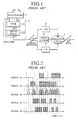
- the binary signal outputted by the precoder 2 is entered into a logical inverter 3.
- This logical inverter 3 outputs a non-inverted signal and an inverted signal which have phases differing by 180° each other.
- These non-inverted signal and inverted signal are converted into a non-inverted duobinary signal and an inverted duobinary signal through separately provided low pass filters (LPF) 4 and 5 respectively, and applied as modulating electric signals to a push-pull type MZ (Mach-Zehnder) modulator 7.
- LPF low pass filters
- a differential encoder for carrying out a precoding with respect to input binary data signals, to obtain encoded signals in which an output logical value is maintained for a first input logical value while an output logical value is inverted for a second input logical value, comprising: an EXOR circuit having one input to which the input binary data signals are entered; and a D-type flip-flop connected to an output of the EXOR circuit and formed by a master latch and a slave latch, an output of the master latch being fed back to another input of the EXOR circuit while also entered into the slave latch, and an output of the slave latch being outputted as an output of the differential encoder.
- Fig. 5 shows a schematic configuration of a precoding-multiplexing circuit in this first embodiment
- Fig. 6 shows a detailed configuration of the precoding-multiplexing circuit of Fig. 5.
- Fig. 7 shows one exemplary configuration of a multi-input EXOR circuit used in the configuration of Fig. 6,
- Fig. 8 shows another exemplary configuration of a multi-input EXOR circuit used in the configuration of Fig. 6.
- the electric signals that are time division multiplexed and encoded are entered into the logical inverter.
- Output signals 201 outputted by the precoding-multiplexing circuit 200 of Fig. 6 are similar to the electric signals entered into the logical inverter in Fig. 1.
- Input signals 101 inputted into the precoding-multiplexing circuit 200 of Fig. 6 correspond to signals X1 and X2 that are entered into the multiplexer in Fig. 1.
- n is not a number in a form of a power of 2
- the configuration can be correspondingly modified as described above.
- the number n of the input signals 101 is 2, so that the precoding circuit 100A of Fig. 9 uses an EXOR circuit 110C in place of the multi-input EXOR circuit 110 of Fig. 6.
- the differential encoder 120A is formed by an EXOR circuit 121 and a one-bit delay 122.
- the one-bit delay 122 delays the signal for one bit time.
- the output of the one-bit delay 122 is connected to one of the inputs of the EXOR circuit 121.
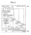
- the precoding-multiplexing circuit 200 of Fig. 6 can be provided in a configuration shown in Fig. 11.
- the precoding-multiplexing circuit 200B shown in Fig. 11 operates as shown in Fig. 12. Note that the delay time of the circuit elements other than a one-bit delay 122 is ignored in Fig. 12. Also, in Fig. 12, regions of the signals for the logical value "1" are depicted as hatched regions, while regions of the signals for the logical value "0" are depicted as blank regions.
- the number n of the input signals 101 is 4, so that the multi-input EXOR circuit. 110 of Fig. 6 is formed by three EXOR circuits.
- the differential encoder 120A is formed similarly as in Fig. 9.
- the precoding circuit 100B of Fig. 11 comprises the multi-input EXOR circuit 110D, the differential encoder 120A and three EXOR circuits 130.
- Four parallel input signals 101(1) to 101(4) in the bit rate which is 1/4 of the transmission rate are entered at the inputs of the precoding circuit 100B of Fig. 11.
- the multi-input EXOR circuit 110D calculates the exclusive OR of all of the four parallel input signals 101(1) to 101(4) and outputs the calculation result as a signal SG1.
- the result of the differential encoding on this signal SG1 is then outputted from the differential encoder 120A as a signal SG3.
- the time division multiplexer 210 arranges four signals SG3, SG4(1), SG4(2), and SG4(3) in order and time division multiplex them, and outputs the obtained result as a signal SG5.
- the signal SG5 outputted by the precoding-multiplexing circuit 200B of Fig. 11 is equivalent to the signal outputted by the conventional precoder.
- the preceding-multiplexing circuit 200C of Fig. 13 comprises a precoding circuit 100C and a selector 215.
- the selector 215 has the same function as the time division multiplexer 210 of the first embodiment.
- the input signal 101(1) is directly entered into one of the inputs of the EXOR circuit 154, while a signal 102(2) obtained by delaying the input signal 101(2) for 1/2 bit time by the half-bit delay 151 is entered into one of the inputs of the EXOR circuit 153. Consequently, there is a half bit phase difference between the signal 101(1) entered into the EXOR circuit 154 and the signal 102(2) entered into the EXOR circuit 153.
- the reset unit 152 outputs a signal for resetting the initial states of the outputs of the two EXOR circuits 153 and 154 to an identical state.
- the initial states of the outputs can be made identical as the reset unit 152 sets the voltage of the current sources of the EXOR circuits 153 and 154 equal to 0.
- the EXOR circuit 161 in response to the first "1" bit of the input signal, in response to the first "1" bit of the input signal, the EXOR circuit 161 inverts the logical value of the output signal (EXOR output) from “0" to "1" after an internal delay time d1. Also, a delay time d2 is required at the D-type flip-flop 160 since reading the signal outputted by the EXOR circuit 161 until outputting it.
- the precoding circuit of Fig. 15 has a configuration in which the signal 162a outputted by the master latch 162 inside the D-type flip-flop 160 is taken out and fed back to the input of the EXOR circuit 161.
- Fig. 17 shows a configuration of the precoding circuit of the fourth embodiment
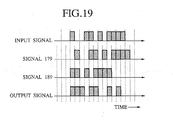
- Fig. 19 shows exemplary signals in the precoding circuit of Fig. 18.
- the precoding circuit shown in Fig. 17 comprises a preliminary processing circuit 170 and a feedback circuit 180.
- the preliminary processing circuit 170 comprises (n-1) sets of one-bit delays (T) 171 and a multi-input EXOR circuit 172.
- the feedback circuit 180 comprises an EXOR circuit 181 and an n-bit delay (nT) 182.
- the encoding is realized by processing electric signals before the time division multiplexing, so that it becomes possible for the precoding circuit to handle signals which are slower than the transmission rate, and therefore it becomes easier to realize the higher transmission rate. This is also effective in eliminating the difficulty of shortening the delay time.
Landscapes
- Physics & Mathematics (AREA)
- Spectroscopy & Molecular Physics (AREA)
- Engineering & Computer Science (AREA)
- Computer Networks & Wireless Communication (AREA)
- Signal Processing (AREA)
- Dc Digital Transmission (AREA)
- Optical Communication System (AREA)
- Time-Division Multiplex Systems (AREA)
Applications Claiming Priority (2)
| Application Number | Priority Date | Filing Date | Title |
|---|---|---|---|
| JP02640899A JP3474794B2 (ja) | 1999-02-03 | 1999-02-03 | 符号変換回路及び符号変換多重化回路 |
| EP00102109A EP1026863B1 (fr) | 1999-02-03 | 2000-02-03 | Circuit de multiplexage à précodage pour systèmes de communication optique |
Related Parent Applications (1)
| Application Number | Title | Priority Date | Filing Date |
|---|---|---|---|
| EP00102109A Division EP1026863B1 (fr) | 1999-02-03 | 2000-02-03 | Circuit de multiplexage à précodage pour systèmes de communication optique |
Publications (2)
| Publication Number | Publication Date |
|---|---|
| EP1830531A1 true EP1830531A1 (fr) | 2007-09-05 |
| EP1830531B1 EP1830531B1 (fr) | 2015-05-06 |
Family
ID=12192736
Family Applications (3)
| Application Number | Title | Priority Date | Filing Date |
|---|---|---|---|
| EP00102109A Expired - Lifetime EP1026863B1 (fr) | 1999-02-03 | 2000-02-03 | Circuit de multiplexage à précodage pour systèmes de communication optique |
| EP20070009325 Expired - Lifetime EP1830532B1 (fr) | 1999-02-03 | 2000-02-03 | Circuit précodé et circuit de multiplexage à précodage pour effectuer un taux de transmission très élevé dans une communication à fibre optique |
| EP20070009323 Expired - Lifetime EP1830531B1 (fr) | 1999-02-03 | 2000-02-03 | Circuit précodé et circuit de multiplexage à précodage pour effectuer un taux de transmission très élevé dans une communication à fibre optique |
Family Applications Before (2)
| Application Number | Title | Priority Date | Filing Date |
|---|---|---|---|
| EP00102109A Expired - Lifetime EP1026863B1 (fr) | 1999-02-03 | 2000-02-03 | Circuit de multiplexage à précodage pour systèmes de communication optique |
| EP20070009325 Expired - Lifetime EP1830532B1 (fr) | 1999-02-03 | 2000-02-03 | Circuit précodé et circuit de multiplexage à précodage pour effectuer un taux de transmission très élevé dans une communication à fibre optique |
Country Status (4)
| Country | Link |
|---|---|
| US (1) | US6934308B1 (fr) |
| EP (3) | EP1026863B1 (fr) |
| JP (1) | JP3474794B2 (fr) |
| DE (1) | DE60045532D1 (fr) |
Cited By (1)
| Publication number | Priority date | Publication date | Assignee | Title |
|---|---|---|---|---|
| WO2009076888A1 (fr) * | 2007-12-14 | 2009-06-25 | Huawei Technologies Co., Ltd. | Système, dispositif et procédé de transmission optique |
Families Citing this family (23)
| Publication number | Priority date | Publication date | Assignee | Title |
|---|---|---|---|---|
| US6490069B1 (en) | 2001-01-29 | 2002-12-03 | Stratalight Communications, Inc. | Transmission and reception of duobinary multilevel pulse-amplitude-modulated optical signals using subtraction-based encoder |
| US6424444B1 (en) | 2001-01-29 | 2002-07-23 | Stratalight Communications, Inc. | Transmission and reception of duobinary multilevel pulse-amplitude-modulated optical signals using finite-state machine-based encoder |
| US6445476B1 (en) | 2001-01-29 | 2002-09-03 | Stratalight Communications, Inc. | Transmission and reception of duobinary multilevel pulse-amplitude-modulated optical signals using subsequence-based encoder |
| JP3597482B2 (ja) * | 2001-03-15 | 2004-12-08 | 三菱電機株式会社 | 多重装置 |
| US6643471B2 (en) | 2001-04-02 | 2003-11-04 | Adc Telecommunications, Inc. | Increased transmission capacity for a fiber-optic link |
| US7287213B1 (en) * | 2001-04-24 | 2007-10-23 | Stratalight Communications, Inc. | Method and system to provide modular parallel precoding in optical duobinary transmission systems |
| US6623188B1 (en) | 2002-02-08 | 2003-09-23 | Optiuh Corporation | Dispersion tolerant optical data transmitter |
| WO2003067790A1 (fr) * | 2002-02-08 | 2003-08-14 | Optium Corporation | Emetteur de donnees optiques tolerant la dispersion |
| US6804472B1 (en) | 2002-11-18 | 2004-10-12 | Stratalight Communications, Inc. | Transmitter and method using half rate data streams for generating full rate modulation on an optical signal |
| KR100547781B1 (ko) * | 2003-06-10 | 2006-01-31 | 삼성전자주식회사 | 편광 듀오바이너리 광전송장치 |
| KR100593998B1 (ko) | 2003-09-25 | 2006-07-03 | 삼성전자주식회사 | 프리코더 및 이를 이용한 광 듀오바이너리 전송장치 |
| US7057538B1 (en) * | 2005-01-10 | 2006-06-06 | Northrop Grumman Corporation | 1/N-rate encoder circuit topology |
| CN101213775B (zh) * | 2005-06-28 | 2013-06-19 | 日本电气株式会社 | Dpsk调制-解调方法及使用该方法的光通信设备和系统 |
| JP4675721B2 (ja) | 2005-08-31 | 2011-04-27 | 三菱電機株式会社 | パラレルプリコーダ回路 |
| JP4597820B2 (ja) * | 2005-09-05 | 2010-12-15 | 三菱電機株式会社 | パラレルプリコーダ回路 |
| FR2892581B1 (fr) * | 2005-10-21 | 2008-01-04 | Alcatel Sa | Multiplexeur a haut debit a architecture parallele |
| US8503568B1 (en) * | 2006-09-07 | 2013-08-06 | The Boeing Company | Differential encoding for multiplexed data streams |
| JP5245736B2 (ja) * | 2008-11-10 | 2013-07-24 | 富士通株式会社 | プリコーダ回路 |
| JP2011166536A (ja) * | 2010-02-10 | 2011-08-25 | Sharp Corp | 無線送信装置、基地局装置、無線送信方法、基地局装置の制御プログラムおよび集積回路 |
| US9294321B2 (en) * | 2010-05-14 | 2016-03-22 | The Boeing Company | Bit signal structure for differentially encoded broadcasts |
| US8717205B2 (en) * | 2010-12-06 | 2014-05-06 | Mitsubishi Electric Corporation | Parallel differential encoding circuits |
| CN105594129A (zh) | 2013-10-03 | 2016-05-18 | 富士通株式会社 | 程序、编码装置以及编码方法 |
| US11789897B2 (en) * | 2020-10-27 | 2023-10-17 | BOE Technology Development Co., Ltd. | Data processing circuit, data processing method, and electronic device |
Citations (5)
| Publication number | Priority date | Publication date | Assignee | Title |
|---|---|---|---|---|
| US4092491A (en) | 1977-04-04 | 1978-05-30 | Bell Telephone Laboratories, Incorporated | Differential encoding and decoding scheme for digital transmission systems |
| US4937577A (en) | 1986-02-14 | 1990-06-26 | Microchip Technology Inc. | Integrated analog-to-digital converter |
| EP0471130B1 (fr) | 1990-08-16 | 1995-12-06 | International Business Machines Corporation | Méthode de codage et dispositif de traitement en parallèle et en pipeline |
| EP0847169A2 (fr) | 1996-12-05 | 1998-06-10 | HE HOLDINGS, INC. dba HUGHES ELECTRONICS | Processeurs et méthodes de communication de signaux compatibles avec plusieurs types de modulation |
| EP1005201A2 (fr) | 1998-11-25 | 2000-05-31 | Fujitsu Limited | Conversion de code pour transmission duobinaire optique |
Family Cites Families (19)
| Publication number | Priority date | Publication date | Assignee | Title |
|---|---|---|---|---|
| US3760109A (en) * | 1971-11-15 | 1973-09-18 | Nissan Motor | Time division multiplex transmission system |
| US3846787A (en) * | 1972-08-17 | 1974-11-05 | Itt | Time division multiplexer employing digital gates and a digital-to-analog converter |
| DE2242639C3 (de) * | 1972-08-30 | 1980-01-17 | Siemens Ag, 1000 Berlin Und 8000 Muenchen | Zeitmultiplex-Telegrafie-System für zeichenweise Verschachtelung |
| US3995119A (en) * | 1975-05-30 | 1976-11-30 | Gte Automatic Electric Laboratories Incorporated | Digital time-division multiplexing system |
| JPS5224410A (en) * | 1975-08-20 | 1977-02-23 | Fujitsu Ltd | Carrier wave regenerative circuit |
| US4630263A (en) * | 1983-07-07 | 1986-12-16 | Motorola, Inc. | Time-division multiplex communications control system |
| IT1199815B (it) * | 1986-12-19 | 1989-01-05 | Rai Radiotelevisione Italiana | Procedimento per la radiodiffusione di segnali digitali,particolarmente di programmi e dati per elaboratori,e procedimento e apparato per la ricezione di tali segnali |
| US4926423A (en) * | 1988-09-30 | 1990-05-15 | The Trustees Of Columbia University In The City Of New York | Time-division-multiplexed data transmission system |
| JPH0771055B2 (ja) * | 1990-08-20 | 1995-07-31 | 株式会社東芝 | 高速度信号多重化装置 |
| US5111455A (en) * | 1990-08-24 | 1992-05-05 | Avantek, Inc. | Interleaved time-division multiplexor with phase-compensated frequency doublers |
| US5148383A (en) * | 1990-12-21 | 1992-09-15 | Amp Incorporated | Digital transversal filter |
| US5282210A (en) * | 1992-06-01 | 1994-01-25 | International Business Machines Corporation | Time-division-multiplexed data transmission system |
| JP3247937B2 (ja) * | 1992-09-24 | 2002-01-21 | 株式会社日立製作所 | 論理集積回路 |
| EP0701338B1 (fr) | 1994-09-12 | 2003-07-23 | Nippon Telegraph And Telephone Corporation | Système de transmission optique à modulation d'intensité |
| JP3306573B2 (ja) | 1994-09-12 | 2002-07-24 | 日本電信電話株式会社 | 光送信装置および光伝送システム |
| JP3276052B2 (ja) | 1996-02-28 | 2002-04-22 | 日本電信電話株式会社 | 光送信装置およびそれを用いた光伝送システム |
| JP2813774B2 (ja) | 1996-11-26 | 1998-10-22 | 郵政省通信総合研究所長 | 光符号分割多重伝送アクセス方式及び装置 |
| JP3011235B2 (ja) | 1997-10-14 | 2000-02-21 | 日本電気株式会社 | 符号変換機能を備えた2値信号多重装置及び符号変換機能を備えた2値信号分離装置 |
| US6243847B1 (en) * | 1998-12-18 | 2001-06-05 | Texas Instruments Incorporated | Parity insertion with precoder feedback in a PRML read channel |
-
1999
- 1999-02-03 JP JP02640899A patent/JP3474794B2/ja not_active Expired - Lifetime
-
2000
- 2000-02-02 US US09/496,974 patent/US6934308B1/en not_active Expired - Lifetime
- 2000-02-03 EP EP00102109A patent/EP1026863B1/fr not_active Expired - Lifetime
- 2000-02-03 EP EP20070009325 patent/EP1830532B1/fr not_active Expired - Lifetime
- 2000-02-03 EP EP20070009323 patent/EP1830531B1/fr not_active Expired - Lifetime
- 2000-02-03 DE DE60045532T patent/DE60045532D1/de not_active Expired - Lifetime
Patent Citations (5)
| Publication number | Priority date | Publication date | Assignee | Title |
|---|---|---|---|---|
| US4092491A (en) | 1977-04-04 | 1978-05-30 | Bell Telephone Laboratories, Incorporated | Differential encoding and decoding scheme for digital transmission systems |
| US4937577A (en) | 1986-02-14 | 1990-06-26 | Microchip Technology Inc. | Integrated analog-to-digital converter |
| EP0471130B1 (fr) | 1990-08-16 | 1995-12-06 | International Business Machines Corporation | Méthode de codage et dispositif de traitement en parallèle et en pipeline |
| EP0847169A2 (fr) | 1996-12-05 | 1998-06-10 | HE HOLDINGS, INC. dba HUGHES ELECTRONICS | Processeurs et méthodes de communication de signaux compatibles avec plusieurs types de modulation |
| EP1005201A2 (fr) | 1998-11-25 | 2000-05-31 | Fujitsu Limited | Conversion de code pour transmission duobinaire optique |
Non-Patent Citations (8)
| Title |
|---|
| HONG-YEAN H. ET AL.: "Proceedings of the International Conference on Computer Design: VLSI in Computers and Processors", IEEE COMPUT. SOC, pages 680 - 685 |
| HONG-YEAN HSIEH ET AL: "Concurrent timing optimization of latch-based digital systems", COMPUTER DESIGN: VLSI IN COMPUTERS AND PROCESSORS, 1995. ICCD '95. PROCEEDINGS., 1995 IEEE INTERNATIONAL CONFERENCE ON AUSTIN, TX, USA 2-4 OCT. 1995, LOS ALAMITOS, CA, USA,IEEE COMPUT. SOC, US, 2 October 1995 (1995-10-02), pages 680 - 685, XP010197383, ISBN: 0-8186-7165-3 * |
| SHENOY N ET AL: "Retiming of circuits with single phase transparent latches", PROCEEDINGS OF THE INTERNATIONAL CONFERENCE ON COMPUTER DESIGN - VLSI IN COMPUTERS AND PROCESSORS. CAMBRIDGE, MA., OCT. 14 - 16, 1991, LOS ALAMITOS, IEEE. COMP. SOC. PRESS, US, 14 October 1991 (1991-10-14), pages 86 - 89, XP010025184, ISBN: 0-8186-2270-9 * |
| SHENOY. N ET AL.: "Proceedings of the International Conference on Computer Design - VLSI in Computers and Processors, IEEE", COMP. SOC. PRESS, article "Retiming of circuits with single phase transparent latches", pages: 86 - 89 |
| WESTE N. H. E. ET AL.: "Principles of CMOS VLSI Design.- A Systems Perspective", ADDISON-WESLEY PUBLISHING COMPANY |
| WESTE N. H. E.; ESHRAGHIAN K.: "PRINCIPLES OF CMOS VLSI DESIGN. - A SYSTEMS PERSPECTIVE", October 1994, ADDISON-WESLEY PUBLISHING COMPANY, US, XP002367338 * |
| YONENAGA ET AL.: "Dispersion-Tolerant Optical Transmission System Using Duobinary Transmitter and Binary Receiver", JOURNAL OF LIGHTWAVE TECHNOLOGY, IEEE, vol. 15, no. 8, 1 August 1997 (1997-08-01), pages 1530 - 1537 |
| YONENAGA K ET AL: "DISPERSION-TOLERANT OPTICAL TRANSMISSION SYSTEM USING DUOBINARY TRANSMITTER AND BINARY RECEIVER", JOURNAL OF LIGHTWAVE TECHNOLOGY, IEEE. NEW YORK, US, vol. 15, no. 8, 1 August 1997 (1997-08-01), pages 1530 - 1537, XP000720478, ISSN: 0733-8724 * |
Cited By (1)
| Publication number | Priority date | Publication date | Assignee | Title |
|---|---|---|---|---|
| WO2009076888A1 (fr) * | 2007-12-14 | 2009-06-25 | Huawei Technologies Co., Ltd. | Système, dispositif et procédé de transmission optique |
Also Published As
| Publication number | Publication date |
|---|---|
| EP1026863A2 (fr) | 2000-08-09 |
| EP1026863B1 (fr) | 2011-01-19 |
| US6934308B1 (en) | 2005-08-23 |
| EP1026863A3 (fr) | 2006-04-12 |
| JP2000224244A (ja) | 2000-08-11 |
| EP1830532A1 (fr) | 2007-09-05 |
| DE60045532D1 (de) | 2011-03-03 |
| JP3474794B2 (ja) | 2003-12-08 |
| EP1830532B1 (fr) | 2015-04-22 |
| EP1830531B1 (fr) | 2015-05-06 |
Similar Documents
| Publication | Publication Date | Title |
|---|---|---|
| EP1830532B1 (fr) | Circuit précodé et circuit de multiplexage à précodage pour effectuer un taux de transmission très élevé dans une communication à fibre optique | |
| US5200979A (en) | High speed telecommunication system using a novel line code | |
| EP1379042B1 (fr) | Multiplexeur | |
| EP2441247B1 (fr) | Transmission de signal optique tmds hdmi utilisant une technique pam | |
| JP2538524B2 (ja) | 信号復号方法および装置 | |
| JP4441275B2 (ja) | ダイレクト光学n相位相シフトキーイングを用いたエンコーダ、そのシステム及びエンコード方法 | |
| US5097353A (en) | Optical repeater having phase inversion circuit | |
| US20080181329A1 (en) | Data transmitting apparatus and data receiving apparatus | |
| JP2005168023A (ja) | デュオバイナリエンコーダ及びこれを用いた光デュオバイナリ伝送装置 | |
| Jameel | Manchester coding and decoding generation theortical and expermental design | |
| JP3447965B2 (ja) | 光送信装置 | |
| US7236702B2 (en) | Method and system for duobinary coding of optical signals | |
| US7057538B1 (en) | 1/N-rate encoder circuit topology | |
| US8750723B2 (en) | Generation of a full-rate optical duobinary signal using half-rate electrical binary signals | |
| US8502711B2 (en) | Swap tolerant coding and decoding circuits and methods | |
| US20070075880A1 (en) | Coding circuit and coding apparatus | |
| JP4701949B2 (ja) | 位相情報発生装置、位相情報発生方法、送信機および受信機 | |
| JPS63284955A (ja) | 光伝送方式 | |
| WO2007022708A1 (fr) | Systeme et procede de generation de signaux optiques de remise a zero avec decalage biphase alternatif et fluctuation de frequence | |
| US20070089026A1 (en) | Coding circuit and coding apparatus | |
| JP4627283B2 (ja) | 光信号処理回路 | |
| WO2005091534A1 (fr) | Systeme de transmission duobinaire optique, et procede associe | |
| JPS63284957A (ja) | 光伝送方式 | |
| JP2006054650A (ja) | 光通信方法 | |
| JP2004140744A (ja) | 符号変換回路、及び光送信回路 |
Legal Events
| Date | Code | Title | Description |
|---|---|---|---|
| PUAI | Public reference made under article 153(3) epc to a published international application that has entered the european phase |
Free format text: ORIGINAL CODE: 0009012 |
|
| 17P | Request for examination filed |
Effective date: 20070509 |
|
| AC | Divisional application: reference to earlier application |
Ref document number: 1026863 Country of ref document: EP Kind code of ref document: P |
|
| AK | Designated contracting states |
Kind code of ref document: A1 Designated state(s): DE FR GB |
|
| RIN1 | Information on inventor provided before grant (corrected) |
Inventor name: MURATA, KOICHI Inventor name: YONEYAMA, MIKIO Inventor name: YONENAGA, KAZUSHIGE Inventor name: MIYAMOTO, YUTAKA |
|
| AKX | Designation fees paid |
Designated state(s): DE FR GB |
|
| 17Q | First examination report despatched |
Effective date: 20120206 |
|
| GRAP | Despatch of communication of intention to grant a patent |
Free format text: ORIGINAL CODE: EPIDOSNIGR1 |
|
| INTG | Intention to grant announced |
Effective date: 20140728 |
|
| GRAP | Despatch of communication of intention to grant a patent |
Free format text: ORIGINAL CODE: EPIDOSNIGR1 |
|
| INTG | Intention to grant announced |
Effective date: 20141016 |
|
| GRAP | Despatch of communication of intention to grant a patent |
Free format text: ORIGINAL CODE: EPIDOSNIGR1 |
|
| INTG | Intention to grant announced |
Effective date: 20141218 |
|
| GRAS | Grant fee paid |
Free format text: ORIGINAL CODE: EPIDOSNIGR3 |
|
| GRAA | (expected) grant |
Free format text: ORIGINAL CODE: 0009210 |
|
| AC | Divisional application: reference to earlier application |
Ref document number: 1026863 Country of ref document: EP Kind code of ref document: P |
|
| AK | Designated contracting states |
Kind code of ref document: B1 Designated state(s): DE FR GB |
|
| REG | Reference to a national code |
Ref country code: GB Ref legal event code: FG4D |
|
| REG | Reference to a national code |
Ref country code: DE Ref legal event code: R096 Ref document number: 60048950 Country of ref document: DE Effective date: 20150618 |
|
| REG | Reference to a national code |
Ref country code: DE Ref legal event code: R097 Ref document number: 60048950 Country of ref document: DE |
|
| REG | Reference to a national code |
Ref country code: FR Ref legal event code: PLFP Year of fee payment: 17 |
|
| PLBE | No opposition filed within time limit |
Free format text: ORIGINAL CODE: 0009261 |
|
| STAA | Information on the status of an ep patent application or granted ep patent |
Free format text: STATUS: NO OPPOSITION FILED WITHIN TIME LIMIT |
|
| 26N | No opposition filed |
Effective date: 20160209 |
|
| REG | Reference to a national code |
Ref country code: FR Ref legal event code: PLFP Year of fee payment: 18 |
|
| REG | Reference to a national code |
Ref country code: FR Ref legal event code: PLFP Year of fee payment: 19 |
|
| PGFP | Annual fee paid to national office [announced via postgrant information from national office to epo] |
Ref country code: DE Payment date: 20190219 Year of fee payment: 20 Ref country code: GB Payment date: 20190218 Year of fee payment: 20 |
|
| PGFP | Annual fee paid to national office [announced via postgrant information from national office to epo] |
Ref country code: FR Payment date: 20190220 Year of fee payment: 20 |
|
| REG | Reference to a national code |
Ref country code: DE Ref legal event code: R071 Ref document number: 60048950 Country of ref document: DE |
|
| REG | Reference to a national code |
Ref country code: GB Ref legal event code: PE20 Expiry date: 20200202 |
|
| PG25 | Lapsed in a contracting state [announced via postgrant information from national office to epo] |
Ref country code: GB Free format text: LAPSE BECAUSE OF EXPIRATION OF PROTECTION Effective date: 20200202 |