EP1832985A2 - Circuit reconfigurable - Google Patents
Circuit reconfigurable Download PDFInfo
- Publication number
- EP1832985A2 EP1832985A2 EP06121240A EP06121240A EP1832985A2 EP 1832985 A2 EP1832985 A2 EP 1832985A2 EP 06121240 A EP06121240 A EP 06121240A EP 06121240 A EP06121240 A EP 06121240A EP 1832985 A2 EP1832985 A2 EP 1832985A2
- Authority
- EP
- European Patent Office
- Prior art keywords
- terminal
- arithmetic unit
- control signal
- unit group
- output terminal
- Prior art date
- Legal status (The legal status is an assumption and is not a legal conclusion. Google has not performed a legal analysis and makes no representation as to the accuracy of the status listed.)
- Granted
Links
Images


Classifications
-
- G—PHYSICS
- G06—COMPUTING OR CALCULATING; COUNTING
- G06F—ELECTRIC DIGITAL DATA PROCESSING
- G06F15/00—Digital computers in general; Data processing equipment in general
- G06F15/76—Architectures of general purpose stored program computers
- G06F15/78—Architectures of general purpose stored program computers comprising a single central processing unit
- G06F15/7867—Architectures of general purpose stored program computers comprising a single central processing unit with reconfigurable architecture
Definitions
- the present invention relates to a reconfigurable circuit.
- FIG. 8 shows a diagram illustrating a configuration example of a reconfigurable circuit in which a configuration 0 is set
- FIG. 9 shows a diagram illustrating a configuration example of a reconfigurable circuit in which a configuration 1 is set.
- the reconfigurable circuit includes a network module 801.
- the network module 801 receives the input data of external input data terminals DI and outputs data from external output data terminals DO.
- the network module 801 includes a first ALU (arithmetic and logic unit) 811, a second ALU 812, a third ALU 813, a fourth ALU 814, a counter 815 and a RAM 816.
- ALU arithmetic and logic unit
- Each ALU 811-814 receives the input data of input terminals (a) and (b), and outputs an arithmetic result from an output terminal (o).
- the counter 815 receives the input data of input terminals (a) and (b), and outputs a counter value from an output terminal (o).
- the RAM 816 receives the input signals of a write terminal 'write' and a read terminal 'read', and outputs data from an output terminal (o) .
- the external input data terminals DI are connected to the input terminals (a) and (b) of the first ALU 811.
- the first ALU 811 adds data of the input terminals (a) and (b).
- the output terminal (o) of the first ALU 811 is connected to the input terminal (a) of the third ALU 813.
- the third ALU 813 performs a 4-bit shift operation of the data of the input terminal (a).
- the output terminal (o) of the third ALU 813 is connected to a 'write' terminal of the RAM 816.
- the RAM 816 performs, for example, a write operation.
- the external input data terminals DI are connected to the input terminal (a) of the fourth ALU 814 and the input terminal (a) of the counter 815.
- the output terminal (o) of the counter 815 is connected to the read terminal 'read' of the RAM 816.
- the RAM 816 performs, for example, a read operation.
- the output terminal (o) of the RAM 816 is connected to the input terminal (b) of the fourth ALU 814.
- the fourth ALU 814 multiplies data of the input terminals (a) and (b).
- the output terminal (o) of the fourth ALU 814 is connected to external output data terminals DO.
- FIG. 10 shows a diagram illustrating a configuration example of the network module 801.
- the network module 801 includes four (4) first switches 1001 and four (4) second switches 1002, and controls the switches 1001, 1002 based on a 64-bit control signal SEL.
- Each of switches 1001 and 1002 includes four input terminals and four output terminals, and can select one of the data input of the four input terminals and output the selected data from each output terminal.
- the 64-bit control signal SEL includes eight (8) 8-bit control signals.
- the eight switches 1001 and 1002 respectively perform control based on the eight 8-bit control signals.
- the input terminals of the first switch 1001 are connected to the above-mentioned arithmetic units 811-816 and the external input data terminals DI.
- the output terminals of the first switch 1001 are connected to the input terminals of the second switch 1002.
- the output terminals of the second switch 1002 are connected to the input terminals of the arithmetic units 811-816 and the external output data
- the network module 801 can switch the functions of the arithmetic units 811-816 by switching the connections among the arithmetic units 811-816 according to the control signals SEL for configuration setting.
- Patent document 1 there is described a semiconductor integrated circuit including an input switch connected to a plurality of data input nodes, an output switch connected to a plurality of data output nodes, a first data path having an arithmetic unit and a first data holding circuit disposed between the above input switch and the above output switch, and a second data path having a second data holding circuit disposed between the input switch and the output switch, in which the first data holding circuit stores arithmetic result data of the arithmetic unit and the second data holding circuit holds data being input to any of the plurality of data input nodes.
- Patent document 2 there is described a semiconductor integrated circuit device having an embedded nonvolatile memory devices, a plurality of processors enabling functional modification by rewriting the memory devices and a unit for interconnecting the above plurality of processors in a programmable manner, formed on a single semiconductor substrate.
- the network module 801 can connect from the output terminals of each arithmetic unit 811-816 to the input terminals of each arithmetic unit 811-816 arbitrarily for any combinations.
- it is configured such that the wirings are used in common so as to reduce both the number of bits of the control signal SEL and the circuit scale.
- the wirings are used in common so as to reduce both the number of bits of the control signal SEL and the circuit scale.
- a reconfigurable circuit including an arithmetic unit group performing arithmetic operations, a network circuit controlling connections among the output terminals and the input terminals of the arithmetic unit group, and a first selector connected between the arithmetic unit group and the network circuit.
- the above arithmetic unit group includes a first terminal and a second terminal
- the above network circuit includes a first terminal and a second terminal
- the first selector connects the first terminal of the arithmetic unit group to the first terminal of the network circuit, and also connects the second terminal of the arithmetic unit group to the second terminal of the network circuit, while when a first control signal is in a second state, the first selector connects the first terminal of the arithmetic unit group to the second terminal of the network circuit, and also connects the second terminal of the arithmetic unit group to the first terminal of the network circuit.
- FIG. 11 shows a diagram illustrating a configuration example simplified from the network module 801 shown in FIG. 10.
- First switches 1101 and 1102 are configured by simplifying the first switches 1001 shown in FIG. 10.
- Second switches 1111 and 1112 are configured by simplifying the second switches 1002 shown in FIG. 10.
- Each of the switches 1101 and 1102 includes two input terminals and two output terminals, respectively, and it is possible to select one of the data of the two input terminals, and output the selected data from each output terminal.
- Each of the switches 1111 and 1112 includes two input terminals and four output terminals, respectively, and it is possible to select one of the data of the two input terminals, and output the selected data from each output terminal.
- the two input terminals of the switch 1101 are connected to an output terminal ALU3o of the third ALU 813 and an output terminal RAMo of the RAM 816, respectively shown in FIG. 8.
- the two output terminals of the switch 1101 one is connected to an input terminal of the switch 1111, while the other is connected to an input terminal of the switch 1112.
- the two input terminals of the switch 1102 are connected to an output terminal ALU1o of the first ALU 811 and an output terminal ALU2o of the second ALU 812, respectively shown in FIG. 8.
- the two output terminals of the switch 1102 one is connected to an input terminal of the switch 1111, while the other is connected to an input terminal of the switch 1112.
- the four output terminals of the switch 1111 are connected to a first input terminal ALU1a of the first ALU 811, a second input terminal ALU1b of the first ALU 811, a first input terminal ALU2a of the second ALU 812, and a second input terminal ALU2b of the second ALU 812, respectively shown in FIG. 8.
- the four output terminals of the switch 1112 are connected to a first input terminal ALU3a of the third ALU 813, a second input terminal ALU3b of the third ALU 813, a write terminal 'RAMwrite' of the RAM 816, and a read terminal 'RAMread' of the RAM 816, respectively shown in FIG. 8.
- the network module 801 connects the output terminal ALU3o to the input terminal ALU1a, and also connects the output terminal RAMo to the input terminal ALU2a.
- the output terminal ALU3o is connectable to the input terminal ALU1a via the switches 1101 and 1111.
- the output terminal RAMo is also connectable to the input terminal ALU2a via the switches 1101 and 1111. Since there is only one connection path between the switches 1101 and 1111, the path between the terminals ALU3o and ALU1a competes with the path between the terminals RAMo and ALU2a at an output terminal 1120 of the switch 1101. As a result, it is not possible to simultaneously connect both the path between the terminals ALU3o and ALU1a and the path between the terminals RAMo and ALU2a.
- FIG. 12 shows a diagram illustrating a circuit in which the output terminals RAMo and ALU1o in the circuit shown in FIG. 11 are exchanged.
- the network module 801 connects the output terminal ALU3o and the input terminal ALU1a, and also connects the output terminal RAMo and the input terminal ALU2a.
- the output terminal ALU3o is connected to the input terminal ALU1a via the switches 1101 and 1111.
- the output terminal RAMo is also connected to the input terminal ALU2a via the switches 1102 and 1111. Since one connection path exists between the switches 1101 and 1111, and another connection path exists between the switches 1102 and 1111, it is possible to connect both paths between the terminals ALU3o and ALU1a and between the terminals RAMo and ALU2a, simultaneously.
- data collision may possibly occur in the network module 801.
- FIG. 12 it is possible to modify the connections between the network module 801 and the arithmetic units.
- the output terminals of the arithmetic units are fixed by hardware, the positions thereof cannot be exchanged. Therefore, according to the present embodiment, by exchanging the connections of the signal lines of the output terminals RAMo and ALU1o of the arithmetic unit, data collision in the network module 801 is avoided, as shown in FIG. 12.
- FIG. 1 shows a diagram illustrating a configuration example of a reconfigurable circuit according to the embodiment of the present invention.
- the reconfigurable circuit can be switched to either the circuit shown in FIG. 8 or the circuit shown in FIG. 9 by means of configuration settings.
- a CPU 101 is connected to a CPU interface 103 via a CPU bus 102.
- a configuration RAM 104 is a network memory, which is connected to the CPU 101 via the CPU bus 102 and the CPU interface 103. Also, the configuration RAM 104 stores network control signal information (configuration data) for 64 planes: a configuration 0 to a configuration 63. The network control signal information has N bits for one plane. The CPU 101 can write the network control signal information for 64 planes in the configuration RAM 104, in advance.
- the CPU 101 When setting, for example, the configuration 0 shown in FIG. 8, the CPU 101 outputs the address of the configuration 0 to the configuration RAM 104. Then, the configuration RAM 104 outputs N-bit network control signal information for the configuration 0 to a network circuit 105.
- the CPU 101 when setting, for example, the configuration 1 shown in FIG. 9, the CPU 101 outputs the address of the configuration 1 to the configuration RAM 104. Then, the configuration RAM 104 outputs N-bit network control signal information for the configuration 1 to the network circuit 105.
- the configuration RAM 104 can dynamically modify the configuration by outputting N-bit network control signal information to the network circuit 105, according to the configuration address being input from the CPU 101.
- An arithmetic unit group includes (n) arithmetic units 111-11n for performing arithmetic operation.
- the network circuit 105 controls (dynamically switches the combinations of) the connections between the output terminals of the (n) arithmetic units 111-11n and the input terminals of the (n) arithmetic units 111-11n. The details thereof will be described later referring to FIG. 2.
- a selector 106 is connected between the output terminals of the (n) arithmetic units 111-11n and the input terminals of the network circuit 105, and thereby the connections between the output terminals of the (n) arithmetic units 111-11n and the input terminals of the network circuit 105 can be exchanged.
- a selector 107 is connected between the input terminals of the (n) arithmetic units 111-11n and the output terminals of the network circuit 105, and thereby the connections between the input terminals of the (n) arithmetic units 111-11n and the output terminals of the network circuit 105 can be exchanged. With this, data collision in the network circuit 105 can be avoided, as shown in FIG. 12.
- FIG. 2 shows a diagram illustrating a configuration example of the network circuit 105.
- the network circuit 105 includes first switches 201-208, second switches 211-218 and third switches 221-228.
- Each first switch 201-208 includes four input terminals and four output terminals, and can select and output either one of the four input terminal data from each output terminal.
- Each second switch 211-218 includes four input terminals and two output terminals, and can select and output either one of the four input terminal data from each output terminal.
- Each third switch 221-228 includes two input terminals and four output terminals, and can select and output either one of the two input terminal data from each output terminal.
- the network circuit 105 includes 32 input terminals in0-in31 and 32 output terminals out0-out31.
- the 32 input terminals in0-in31 are connected to the output terminals of the arithmetic units 111-11n via the selector 106 shown in FIG. 1.
- the 32 output terminals out0-out31 are connected to the input terminals of the arithmetic units 111-11n via the selector 107 shown in FIG. 1.
- the switch 201 the four input terminals thereof are connected to the four input terminals in0-in3, and the four output terminals thereof are connected to the input terminals of the switches 211-214.
- the switch 202 the four input terminals thereof are connected to the four input terminals in4-in7, and the four output terminals thereof are connected to the input terminals of the switches 211-214.
- the switch 203 the four input terminals thereof are connected to the four input terminals in8-in11, and the four output terminals thereof are connected to the input terminals of the switches 211-214.
- the switch 204 the four input terminals thereof are connected to the four input terminals in12-in15, and the four output terminals thereof are connected to the input terminals of the switches 211-214.
- the switch 205 the four input terminals thereof are connected to the four input terminals in16-in19, and the four output terminals thereof are connected to the input terminals of the switches 215-218.
- the switch 206 the four input terminals thereof are connected to the four input terminals in20-in23, and the four output terminals thereof are connected to the input terminals of the switches 215-218.
- the switch 207 the four input terminals thereof are connected to the four input terminals in24-in27, and the four output terminals thereof are connected to the input terminals of the switches 215-218.
- the switch 208 the four input terminals thereof are connected to the four input terminals in28-in31, and the four output terminals thereof are connected to the input terminals of the switches 215-218.
- the two output terminals of the switch 211 are connected to the input terminals of the switches 221, 225.
- the two output terminals of the switch 212 are connected to the input terminals of the switches 222, 226.
- the two output terminals of the switch 213 are connected to the input terminals of the switches 223, 227.
- the two output terminals of the switch 214 are connected to the input terminals of the switches 224, 228.
- the two output terminals of the switch 215 are connected to the input terminals of the switches 221, 225.
- the two output terminals of the switch 216 are connected to the input terminals of the switches 222, 226.
- the two output terminals of the switch 217 are connected to the input terminals of the switches 223, 227.
- the two output terminals of the switch 218 are connected to the input terminals of the switches 224, 228.
- the four output terminals of the switch 221 are connected to the output terminals out0-out3.
- the four output terminals of the switch 222 are connected to the output terminals out4-out7.
- the four output terminals of the switch 223 are connected to the output terminals out8-out11.
- the four output terminals of the switch 224 are connected to the output terminals out12-out15.
- the four output terminals of the switch 225 are connected to the output terminals out16-out19.
- the four output terminals of the switch 226 are connected to the output terminals out20-out23.
- the four output terminals of the switch 227 are connected to the output terminals out24-out27.
- the four output terminals of the switch 228 are connected to the output terminals out28-out31.
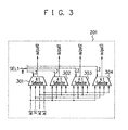
- FIG. 3 shows a diagram illustrating a configuration example of the switch 201.
- the switch 201 includes selectors 301-304. Also, the switch 201 receives the input data of the input terminals in0-in3, and outputs data from output terminals output0-output3, according to a network control signal SEL1.
- the 8-bit network control signal SEL1 is distributed after being divided into four 2-bit signals, and then output to the selectors 301-304.
- the selector 301 receives the input data of the four input terminals in0-in3 according to a 2-bit signal out of the network control signal SEL1, selects and outputs either one of the input data from the output terminal output 0.
- the selector 302 receives the input data of the four input terminals in0-in3 according to a 2-bit signal out of the network control signal SEL1, selects and outputs either one of the input data from the output terminal output1.
- the selector 303 receives the input data of the four input terminals in0-in3 according to a 2-bit signal out of the network control signal SEL1, selects and outputs either one of the input data from the output terminal output2.
- the selector 304 receives the input data of the four input terminals in0-in3 according to a 2-bit signal out of the network control signal SEL1, selects and outputs either one of the input data from the output terminal output3.
- Other switches 202-208, 211-218 and 221-228 have the similar configurations as the switch 201.
- FIG. 4 shows a diagram illustrating a more concrete configuration example of the reconfigurable circuit shown in FIG. 1.
- a register 401 is added to the configuration shown in FIG. 1.
- the register 401 is a flip-flop, which is connected to the CPU 101 via the CPU bus 102 and the CPU interface 103, and stores M-bit selector control signal information.
- the CPU 101 can write selector control signal information having N bits into the register 401.
- the selector 106 can exchange the connections between the output terminals of the arithmetic units 111-11n and the input terminals of the network circuit 105.
- FIG. 5 shows a flowchart illustrating an operation example of the reconfigurable circuit shown in FIG. 4.
- the CPU 101 writes the network control signal information into the configuration RAM 104 via the network interface 103, and writes the selector control signal information into the register 401.
- the above processing is initiation setting processing, which is performed once at the time of initiation.
- the selector 106 connects between the output terminals of the arithmetic units 111-11n and the input terminals of the network circuit 105.
- the selector 107 connects between the input terminals of the arithmetic units 111-11n and the output terminals of the network circuit 105.
- step S502 a core operation of reconfiguration is performed.
- the CPU 101 outputs an address for setting configuration to the configuration RAM 104.
- the configuration RAM 104 outputs network control signal information of the set configuration to the network circuit 105.
- the network circuit 105 connects between the input terminals in0-in31 and the output terminals out0-out31 shown in FIG. 2.
- the configuration RAM 104 sequentially outputs to the network circuit 105 the network control signal information in regard to the configuration 0 to the configuration N.
- the network circuit 105 sequentially performs connections based on the settings of the configuration 0 to the configuration N.
- FIG. 6 shows a diagram illustrating a more concrete configuration example of the reconfigurable circuit shown in FIG. 4.
- a register 402 is added to the configuration shown in FIG. 4.
- the selector 106 includes sixteen (16) swap selectors 601-616.
- the selector 107 includes sixteen (16) swap selectors 617-632.
- the configuration RAM 104 stores network control signal information for 64 planes: the configuration 0 to the configuration 63.
- the network control signal information has 1,024 bits per plane.
- the configuration RAM 104 outputs the 1,024-bit network control signal information to the network circuit 105.
- the network circuit 105 includes 128 input terminals, 128 output terminals and 128 switches. As shown in FIG. 3, each the above switch includes four input terminals and four output terminals, and controls the connections between the four input terminals and the four output terminals according to an 8-bit control signal.
- the register 401 is a flip-flop, which is connected to the CPU 101 via the CPU bus 102 and the CPU interface 103, and stores 64-bit selector control signal information.
- the CPU 101 can write the 64-bit selector control signal information into the register 401.
- the selector 106 can exchange the connections between the output terminals of the arithmetic units 111-11n and the input terminals of the network circuit 105.
- the register 402 is a flip-flop, which is connected to the CPU 101 via the CPU bus 102 and the CPU interface 103, and stores 64-bit selector control signal information.
- the CPU 101 can write the 64-bit selector control signal information into the register 402.
- the selector 107 can exchange the connections between the input terminals of the arithmetic units 111-11n and the output terminals of the network circuit 105.
- FIG. 7 shows a diagram illustrating a configuration example of the swap selector 601.
- the swap selector 601 includes eight (8) input terminals in0-in7, and eight (8) output terminals out0-out7.
- the input terminals in0-in7 are connected to the output terminals of the arithmetic units 111-11n.
- the output terminals out 0-out 7 are connected to the input terminals of the network circuit 105.
- the swap selector 601 exchanges the connections between the eight input terminals in0-in7 and the eight output terminals out0-out7.
- a first bit of the selector control signal When a first bit of the selector control signal is in a first state (for example, '0'), the input terminal in0 is connected to the output terminal out0, and the input terminal in4 is connected to the output terminal out4.
- the first bit of the selector control signal is in a second state (for example, '1')
- the input terminal in 0 is connected to the output terminal out4
- the input terminal in4 is connected to the output terminal out0.
- a third bit of the selector control signal is in a first state (for example, '0')
- the input terminal in2 is connected to the output terminal out2
- the input terminal in6 is connected to the output terminal out 6.
- the second bit of the selector control signal is in a second state (for example, '1')
- the input terminal in2 is connected to the output terminal out6, and the input terminal in6 is connected to the output terminal out2.
- a fourth bit of the selector control signal is in a first state (for example, '0')
- the input terminal in3 is connected to the output terminal out3
- the input terminal in7 is connected to the output terminal out7.
- the second bit of the selector control signal is in a second state (for example, '1')
- the input terminal in3 is connected to the output terminal out7
- the input terminal in7 is connected to the output terminal out3.
- the swap selector 601 when the selector control signal is in the first state, the swap selector 601 performs straight connections without exchanging the connections between the input terminals in0-in7 and the output terminals out0-out7, while when the selector control signal is in the second state, the swap selector 601 performs cross connections by exchanging the connections between the input terminals in0-in7 and the output terminals out0-out7.
- the network control signal information which the configuration RAM 104 outputs to the network circuit 105 has 1,024 bits.
- the configuration RAM 104 stores the network control signal information for 64 planes, a capacity of the order of 64 kbits is required.
- the register 401 includes 64 flip-flops and also the register 402 includes 64 flip-flops. Further, two CPU interfaces 103 are required for the registers 401, 402. Even in case of adding the selectors 106, 107, the circuit scale can be restrained, as compared to the network circuit 105 and the configuration RAM 104.
- the selectors 106, 107 are added to modify the connections between the network circuit 105 and the arithmetic units 111-11n even after the completion of the hardware. More specifically, as shown in FIG. 6, the selector 106 is provided between the output terminals of the arithmetic units 111-11n and the input terminals of the network circuit 105, and also the selector 107 is provided between the input terminals of the arithmetic units 111-11n and the output terminals of the network circuit 105.
- the selector control signals for the selectors 106, 107 are input from the registers 401, 402, instead of being input from the configuration RAM 104.
- the CPU 101 writes the selector control signal information to the registers 401, 402, via the CPU interfaces 103.
- the reason for not using the configuration RAM 104 is that, in addition to the aim at reducing the circuit scale, the connection settings of the arithmetic units 111-11n and the network circuit 105 are assumed to be performed only at the time of initiation setting of the reconfigurable circuit, as shown in FIG. 5. Because the configuration RAM 104 is used when the settings are desired to switch during operation, a capacity of (the number of bits to be set) x (the number of planes of switchover) is required. Therefore, by limiting the portion to be switched over during the operation, and by setting the other portions at the time of initiation by writing from the CPU 101, it becomes possible to improve the degree of freedom in the network connection with a reduced circuit scale.
- the connections between the network module 801 and the arithmetic units are fixed by hardware in the reconfigurable circuit shown in FIG. 11, there may be cases that the intended network connections cannot be attained at the time of connecting between the output terminals and the input terminals of the arithmetic units, due to network routing limitation.
- connection exchanging function of the selectors 106, 107 can be set by the registers 401, 402, it is possible to reduce the circuit scale as compared to the case of using the configuration RAM 104.
- the selectors 106, 107 it becomes possible to reduce the circuit scale, and also increase the number of connectable combinations between the output terminals and the input terminals of the arithmetic unit group.
- the present embodiment is not limited to the case of providing both the selectors 106 and 107. It may be possible to provide the selector 106 only, with the deletion of the selector 107. Or, it may be possible to provide the selector 107 only, with the deletion of the selector 106.
Landscapes
- Engineering & Computer Science (AREA)
- Computer Hardware Design (AREA)
- Theoretical Computer Science (AREA)
- Physics & Mathematics (AREA)
- General Engineering & Computer Science (AREA)
- General Physics & Mathematics (AREA)
- Logic Circuits (AREA)
- Semiconductor Integrated Circuits (AREA)
- Design And Manufacture Of Integrated Circuits (AREA)
Applications Claiming Priority (1)
| Application Number | Priority Date | Filing Date | Title |
|---|---|---|---|
| JP2006065695A JP4782591B2 (ja) | 2006-03-10 | 2006-03-10 | リコンフィグラブル回路 |
Publications (3)
| Publication Number | Publication Date |
|---|---|
| EP1832985A2 true EP1832985A2 (fr) | 2007-09-12 |
| EP1832985A3 EP1832985A3 (fr) | 2008-07-02 |
| EP1832985B1 EP1832985B1 (fr) | 2012-07-04 |
Family
ID=38179882
Family Applications (1)
| Application Number | Title | Priority Date | Filing Date |
|---|---|---|---|
| EP06121240A Not-in-force EP1832985B1 (fr) | 2006-03-10 | 2006-09-26 | Circuit reconfigurable |
Country Status (4)
| Country | Link |
|---|---|
| US (1) | US8099540B2 (fr) |
| EP (1) | EP1832985B1 (fr) |
| JP (1) | JP4782591B2 (fr) |
| CN (1) | CN101034387B (fr) |
Cited By (1)
| Publication number | Priority date | Publication date | Assignee | Title |
|---|---|---|---|---|
| CN102650860A (zh) * | 2011-02-25 | 2012-08-29 | 西安邮电学院 | 一种新型数据流dsp中信号处理硬件的控制器结构 |
Families Citing this family (6)
| Publication number | Priority date | Publication date | Assignee | Title |
|---|---|---|---|---|
| JP4962305B2 (ja) * | 2007-12-26 | 2012-06-27 | 富士通セミコンダクター株式会社 | リコンフィギュラブル回路 |
| JP5115307B2 (ja) * | 2008-04-25 | 2013-01-09 | 富士通セミコンダクター株式会社 | 半導体集積回路 |
| JP5599987B2 (ja) | 2009-06-12 | 2014-10-01 | スパンション エルエルシー | 多重化用補助peおよび半導体集積回路 |
| WO2014110686A1 (fr) * | 2013-01-15 | 2014-07-24 | Micron Technology, Inc. | Boîtier récupérable pour dispositifs à semiconducteurs, et systèmes et procédés associés |
| JP6379032B2 (ja) * | 2014-12-26 | 2018-08-22 | 株式会社メガチップス | 乱数生成装置及び乱数生成方法 |
| US10931282B2 (en) | 2016-06-16 | 2021-02-23 | Board Of Regents, The University Of Texas System | Self-contained reconfigurable personal laboratory |
Family Cites Families (25)
| Publication number | Priority date | Publication date | Assignee | Title |
|---|---|---|---|---|
| US4901268A (en) * | 1988-08-19 | 1990-02-13 | General Electric Company | Multiple function data processor |
| JPH06274459A (ja) | 1993-03-17 | 1994-09-30 | Hitachi Ltd | 半導体集積回路装置 |
| US6265894B1 (en) * | 1995-10-13 | 2001-07-24 | Frederic Reblewski | Reconfigurable integrated circuit with integrated debugging facilities for use in an emulation system |
| US5724276A (en) * | 1996-06-17 | 1998-03-03 | Xilinx, Inc. | Logic block structure optimized for sum generation |
| KR100222032B1 (ko) * | 1996-12-24 | 1999-10-01 | 윤종용 | 디지탈 신호 처리기에서의 2배 정밀도 곱셈연산 수행방법 |
| US6122719A (en) * | 1997-10-31 | 2000-09-19 | Silicon Spice | Method and apparatus for retiming in a network of multiple context processing elements |
| US6745317B1 (en) * | 1999-07-30 | 2004-06-01 | Broadcom Corporation | Three level direct communication connections between neighboring multiple context processing elements |
| TWI234737B (en) * | 2001-05-24 | 2005-06-21 | Ip Flex Inc | Integrated circuit device |
| US6963890B2 (en) * | 2001-05-31 | 2005-11-08 | Koninklijke Philips Electronics N.V. | Reconfigurable digital filter having multiple filtering modes |
| CA2459411C (fr) * | 2001-09-07 | 2013-04-02 | Ip Flex Inc. | Systeme de traitement de donnees et methode de controle connexe |
| US20030055852A1 (en) * | 2001-09-19 | 2003-03-20 | Wojko Mathew Francis | Reconfigurable arithmetic logic block array for FPGAs |
| US6476634B1 (en) * | 2002-02-01 | 2002-11-05 | Xilinx, Inc. | ALU implementation in single PLD logic cell |
| US7627817B2 (en) * | 2003-02-21 | 2009-12-01 | Motionpoint Corporation | Analyzing web site for translation |
| JP4423953B2 (ja) | 2003-07-09 | 2010-03-03 | 株式会社日立製作所 | 半導体集積回路 |
| US7149996B1 (en) * | 2003-07-11 | 2006-12-12 | Xilinx, Inc. | Reconfigurable multi-stage crossbar |
| TW200504592A (en) * | 2003-07-24 | 2005-02-01 | Ind Tech Res Inst | Reconfigurable apparatus with high hardware efficiency |
| JP4603335B2 (ja) * | 2003-11-11 | 2010-12-22 | 株式会社リコー | データ転送システム、画像形成システム及びデータ転送方法 |
| JP4603336B2 (ja) * | 2003-11-11 | 2010-12-22 | 株式会社リコー | データ転送システム、画像形成システム及びデータ転送方法 |
| JP4271558B2 (ja) * | 2003-11-19 | 2009-06-03 | 株式会社リコー | データ転送システム、画像形成システム及びデータ転送用プログラム |
| JP4300151B2 (ja) * | 2004-04-19 | 2009-07-22 | Okiセミコンダクタ株式会社 | 演算処理装置 |
| US20060004902A1 (en) * | 2004-06-30 | 2006-01-05 | Siva Simanapalli | Reconfigurable circuit with programmable split adder |
| JP2006018413A (ja) * | 2004-06-30 | 2006-01-19 | Fujitsu Ltd | プロセッサおよびパイプライン再構成制御方法 |
| JP2006018411A (ja) * | 2004-06-30 | 2006-01-19 | Fujitsu Ltd | プロセッサ |
| US20060114918A1 (en) | 2004-11-09 | 2006-06-01 | Junichi Ikeda | Data transfer system, data transfer method, and image apparatus system |
| US7590676B1 (en) * | 2005-09-27 | 2009-09-15 | Altera Corporation | Programmable logic device with specialized multiplier blocks |
-
2006
- 2006-03-10 JP JP2006065695A patent/JP4782591B2/ja not_active Expired - Fee Related
- 2006-09-26 EP EP06121240A patent/EP1832985B1/fr not_active Not-in-force
- 2006-10-11 US US11/545,477 patent/US8099540B2/en active Active
- 2006-10-25 CN CN2006101375611A patent/CN101034387B/zh not_active Expired - Fee Related
Cited By (1)
| Publication number | Priority date | Publication date | Assignee | Title |
|---|---|---|---|---|
| CN102650860A (zh) * | 2011-02-25 | 2012-08-29 | 西安邮电学院 | 一种新型数据流dsp中信号处理硬件的控制器结构 |
Also Published As
| Publication number | Publication date |
|---|---|
| EP1832985A3 (fr) | 2008-07-02 |
| CN101034387A (zh) | 2007-09-12 |
| CN101034387B (zh) | 2011-12-14 |
| EP1832985B1 (fr) | 2012-07-04 |
| US20070230336A1 (en) | 2007-10-04 |
| JP4782591B2 (ja) | 2011-09-28 |
| JP2007241830A (ja) | 2007-09-20 |
| US8099540B2 (en) | 2012-01-17 |
Similar Documents
| Publication | Publication Date | Title |
|---|---|---|
| JP2642671B2 (ja) | ディジタルクロスバースイッチ | |
| US20220083499A1 (en) | Efficient deconfiguration of a reconfigurable data processor | |
| US4985830A (en) | Interprocessor bus switching system for simultaneous communication in plural bus parallel processing system | |
| US20020095562A1 (en) | Arithmetic unit comprising a memory shared by a plurality of processors | |
| EP1001347A2 (fr) | Dispositif de traitement de données comprenant une unité d'accouplement de mémoire | |
| US5381529A (en) | Shift register with dual clock inputs for receiving and sending information between I/O channels and host based on external and internal clock inputs respectively | |
| AU7600094A (en) | Multiple-port shared memory interface and associated method | |
| JP4485272B2 (ja) | 半導体装置 | |
| EP1832985B1 (fr) | Circuit reconfigurable | |
| KR100450680B1 (ko) | 버스 대역폭을 증가시키기 위한 메모리 컨트롤러, 이를이용한 데이터 전송방법 및 이를 구비하는 컴퓨터 시스템 | |
| CN100397334C (zh) | 半导体器件 | |
| JP4205743B2 (ja) | 半導体記憶装置及び半導体装置 | |
| CN101506784B (zh) | 简单直接存储器存取中的外围供应寻址 | |
| EP1271543A2 (fr) | Méthode et système d'accès mémoire rapide | |
| US5790883A (en) | Multiple ports storage device with programmable overlapped data bits access | |
| US6675283B1 (en) | Hierarchical connection of plurality of functional units with faster neighbor first level and slower distant second level connections | |
| US7519848B2 (en) | Data transfer apparatus | |
| JPH0758755A (ja) | 異なる周波数で動作する通信端子を接続する相互接続ピンメモリ | |
| JP2007148622A (ja) | インターフェース設定方法 | |
| US7310710B1 (en) | Register file with integrated routing to execution units for multi-threaded processors | |
| JP4614501B2 (ja) | 1以上の仮想ポートを規定する構成回路および集積回路 | |
| JP2000076199A (ja) | デバッグ端子を有するマルチプロセッサ装置 | |
| JP2007004424A (ja) | バスシステム | |
| JPH01142849A (ja) | 加入者線信号装置 | |
| JPH03282602A (ja) | シーケンサ回路 |
Legal Events
| Date | Code | Title | Description |
|---|---|---|---|
| PUAI | Public reference made under article 153(3) epc to a published international application that has entered the european phase |
Free format text: ORIGINAL CODE: 0009012 |
|
| AK | Designated contracting states |
Kind code of ref document: A2 Designated state(s): AT BE BG CH CY CZ DE DK EE ES FI FR GB GR HU IE IS IT LI LT LU LV MC NL PL PT RO SE SI SK TR |
|
| AX | Request for extension of the european patent |
Extension state: AL BA HR MK YU |
|
| PUAL | Search report despatched |
Free format text: ORIGINAL CODE: 0009013 |
|
| AK | Designated contracting states |
Kind code of ref document: A3 Designated state(s): AT BE BG CH CY CZ DE DK EE ES FI FR GB GR HU IE IS IT LI LT LU LV MC NL PL PT RO SE SI SK TR |
|
| AX | Request for extension of the european patent |
Extension state: AL BA HR MK RS |
|
| 17P | Request for examination filed |
Effective date: 20081128 |
|
| RAP1 | Party data changed (applicant data changed or rights of an application transferred) |
Owner name: FUJITSU MICROELECTRONICS LIMITED |
|
| AKX | Designation fees paid |
Designated state(s): DE FR IT |
|
| RAP1 | Party data changed (applicant data changed or rights of an application transferred) |
Owner name: FUJITSU SEMICONDUCTOR LIMITED |
|
| GRAP | Despatch of communication of intention to grant a patent |
Free format text: ORIGINAL CODE: EPIDOSNIGR1 |
|
| RIN1 | Information on inventor provided before grant (corrected) |
Inventor name: HANAI, TAKASHI Inventor name: KAWANO, TETSUO |
|
| GRAS | Grant fee paid |
Free format text: ORIGINAL CODE: EPIDOSNIGR3 |
|
| GRAA | (expected) grant |
Free format text: ORIGINAL CODE: 0009210 |
|
| AK | Designated contracting states |
Kind code of ref document: B1 Designated state(s): DE FR IT |
|
| REG | Reference to a national code |
Ref country code: DE Ref legal event code: R096 Ref document number: 602006030524 Country of ref document: DE Effective date: 20120830 |
|
| PLBE | No opposition filed within time limit |
Free format text: ORIGINAL CODE: 0009261 |
|
| STAA | Information on the status of an ep patent application or granted ep patent |
Free format text: STATUS: NO OPPOSITION FILED WITHIN TIME LIMIT |
|
| PG25 | Lapsed in a contracting state [announced via postgrant information from national office to epo] |
Ref country code: IT Free format text: LAPSE BECAUSE OF FAILURE TO SUBMIT A TRANSLATION OF THE DESCRIPTION OR TO PAY THE FEE WITHIN THE PRESCRIBED TIME-LIMIT Effective date: 20120704 |
|
| 26N | No opposition filed |
Effective date: 20130405 |
|
| REG | Reference to a national code |
Ref country code: FR Ref legal event code: ST Effective date: 20130531 |
|
| REG | Reference to a national code |
Ref country code: DE Ref legal event code: R097 Ref document number: 602006030524 Country of ref document: DE Effective date: 20130405 |
|
| PG25 | Lapsed in a contracting state [announced via postgrant information from national office to epo] |
Ref country code: FR Free format text: LAPSE BECAUSE OF NON-PAYMENT OF DUE FEES Effective date: 20121001 |
|
| REG | Reference to a national code |
Ref country code: DE Ref legal event code: R082 Ref document number: 602006030524 Country of ref document: DE Representative=s name: VON KREISLER SELTING WERNER, DE |
|
| REG | Reference to a national code |
Ref country code: DE Ref legal event code: R081 Ref document number: 602006030524 Country of ref document: DE Owner name: SPANSION LLC (N.D.GES.D. STAATES DELAWARE), US Free format text: FORMER OWNER: FUJITSU LTD., KAWASAKI-SHI, JP Effective date: 20120705 Ref country code: DE Ref legal event code: R081 Ref document number: 602006030524 Country of ref document: DE Owner name: SPANSION LLC (N.D.GES.D. STAATES DELAWARE), US Free format text: FORMER OWNER: FUJITSU SEMICONDUCTOR LIMITED, YOKOHAMA-SHI, JP Effective date: 20140331 Ref country code: DE Ref legal event code: R082 Ref document number: 602006030524 Country of ref document: DE Representative=s name: VON KREISLER SELTING WERNER - PARTNERSCHAFT VO, DE Effective date: 20140331 Ref country code: DE Ref legal event code: R081 Ref document number: 602006030524 Country of ref document: DE Owner name: SPANSION LLC (N.D.GES.D. STAATES DELAWARE), SU, US Free format text: FORMER OWNER: FUJITSU SEMICONDUCTOR LIMITED, YOKOHAMA-SHI, KANAGAWA, JP Effective date: 20140331 Ref country code: DE Ref legal event code: R081 Ref document number: 602006030524 Country of ref document: DE Owner name: SPANSION LLC (N.D.GES.D. STAATES DELAWARE), SU, US Free format text: FORMER OWNER: FUJITSU LTD., KAWASAKI-SHI, KANAGAWA-KEN, JP Effective date: 20120705 Ref country code: DE Ref legal event code: R081 Ref document number: 602006030524 Country of ref document: DE Owner name: CYPRESS SEMICONDUCTOR CORP. (N.D.GES.D.STAATES, US Free format text: FORMER OWNER: FUJITSU SEMICONDUCTOR LIMITED, YOKOHAMA-SHI, KANAGAWA, JP Effective date: 20140331 Ref country code: DE Ref legal event code: R081 Ref document number: 602006030524 Country of ref document: DE Owner name: CYPRESS SEMICONDUCTOR CORP. (N.D.GES.D.STAATES, US Free format text: FORMER OWNER: FUJITSU LTD., KAWASAKI-SHI, KANAGAWA-KEN, JP Effective date: 20120705 Ref country code: DE Ref legal event code: R082 Ref document number: 602006030524 Country of ref document: DE Representative=s name: MURGITROYD & COMPANY, DE Effective date: 20140331 Ref country code: DE Ref legal event code: R081 Ref document number: 602006030524 Country of ref document: DE Owner name: CYPRESS SEMICONDUCTOR CORP. (N.D.GES.D.STAATES, US Free format text: FORMER OWNER: FUJITSU LIMITED, KAWASAKI-SHI, KANAGAWA, JP Effective date: 20120705 |
|
| REG | Reference to a national code |
Ref country code: DE Ref legal event code: R082 Ref document number: 602006030524 Country of ref document: DE Representative=s name: MURGITROYD & COMPANY, DE Ref country code: DE Ref legal event code: R081 Ref document number: 602006030524 Country of ref document: DE Owner name: CYPRESS SEMICONDUCTOR CORP. (N.D.GES.D.STAATES, US Free format text: FORMER OWNER: SPANSION LLC (N.D.GES.D. STAATES DELAWARE), SUNNYVALE, CALIF., US |
|
| PGFP | Annual fee paid to national office [announced via postgrant information from national office to epo] |
Ref country code: DE Payment date: 20180920 Year of fee payment: 13 |
|
| REG | Reference to a national code |
Ref country code: DE Ref legal event code: R119 Ref document number: 602006030524 Country of ref document: DE |
|
| PG25 | Lapsed in a contracting state [announced via postgrant information from national office to epo] |
Ref country code: DE Free format text: LAPSE BECAUSE OF NON-PAYMENT OF DUE FEES Effective date: 20200401 |