EP1833092A1 - Bildsensor, der Pixel mit einem Transistor umfasst - Google Patents
Bildsensor, der Pixel mit einem Transistor umfasst Download PDFInfo
- Publication number
- EP1833092A1 EP1833092A1 EP07103611A EP07103611A EP1833092A1 EP 1833092 A1 EP1833092 A1 EP 1833092A1 EP 07103611 A EP07103611 A EP 07103611A EP 07103611 A EP07103611 A EP 07103611A EP 1833092 A1 EP1833092 A1 EP 1833092A1
- Authority
- EP
- European Patent Office
- Prior art keywords
- substrate
- zone
- pixels
- buried
- pixel
- Prior art date
- Legal status (The legal status is an assumption and is not a legal conclusion. Google has not performed a legal analysis and makes no representation as to the accuracy of the status listed.)
- Withdrawn
Links
Images

Classifications
-
- H—ELECTRICITY
- H10—SEMICONDUCTOR DEVICES; ELECTRIC SOLID-STATE DEVICES NOT OTHERWISE PROVIDED FOR
- H10F—INORGANIC SEMICONDUCTOR DEVICES SENSITIVE TO INFRARED RADIATION, LIGHT, ELECTROMAGNETIC RADIATION OF SHORTER WAVELENGTH OR CORPUSCULAR RADIATION
- H10F39/00—Integrated devices, or assemblies of multiple devices, comprising at least one element covered by group H10F30/00, e.g. radiation detectors comprising photodiode arrays
- H10F39/011—Manufacture or treatment of image sensors covered by group H10F39/12
- H10F39/014—Manufacture or treatment of image sensors covered by group H10F39/12 of CMOS image sensors
-
- H—ELECTRICITY
- H10—SEMICONDUCTOR DEVICES; ELECTRIC SOLID-STATE DEVICES NOT OTHERWISE PROVIDED FOR
- H10F—INORGANIC SEMICONDUCTOR DEVICES SENSITIVE TO INFRARED RADIATION, LIGHT, ELECTROMAGNETIC RADIATION OF SHORTER WAVELENGTH OR CORPUSCULAR RADIATION
- H10F39/00—Integrated devices, or assemblies of multiple devices, comprising at least one element covered by group H10F30/00, e.g. radiation detectors comprising photodiode arrays
- H10F39/10—Integrated devices
- H10F39/12—Image sensors
- H10F39/18—Complementary metal-oxide-semiconductor [CMOS] image sensors; Photodiode array image sensors
- H10F39/186—Complementary metal-oxide-semiconductor [CMOS] image sensors; Photodiode array image sensors having arrangements for blooming suppression
-
- H—ELECTRICITY
- H10—SEMICONDUCTOR DEVICES; ELECTRIC SOLID-STATE DEVICES NOT OTHERWISE PROVIDED FOR
- H10F—INORGANIC SEMICONDUCTOR DEVICES SENSITIVE TO INFRARED RADIATION, LIGHT, ELECTROMAGNETIC RADIATION OF SHORTER WAVELENGTH OR CORPUSCULAR RADIATION
- H10F39/00—Integrated devices, or assemblies of multiple devices, comprising at least one element covered by group H10F30/00, e.g. radiation detectors comprising photodiode arrays
- H10F39/80—Constructional details of image sensors
-
- H—ELECTRICITY
- H10—SEMICONDUCTOR DEVICES; ELECTRIC SOLID-STATE DEVICES NOT OTHERWISE PROVIDED FOR
- H10F—INORGANIC SEMICONDUCTOR DEVICES SENSITIVE TO INFRARED RADIATION, LIGHT, ELECTROMAGNETIC RADIATION OF SHORTER WAVELENGTH OR CORPUSCULAR RADIATION
- H10F39/00—Integrated devices, or assemblies of multiple devices, comprising at least one element covered by group H10F30/00, e.g. radiation detectors comprising photodiode arrays
- H10F39/80—Constructional details of image sensors
- H10F39/803—Pixels having integrated switching, control, storage or amplification elements
- H10F39/8037—Pixels having integrated switching, control, storage or amplification elements the integrated elements comprising a transistor
- H10F39/80377—Pixels having integrated switching, control, storage or amplification elements the integrated elements comprising a transistor characterised by the channel of the transistor, e.g. channel having a doping gradient
-
- H—ELECTRICITY
- H10—SEMICONDUCTOR DEVICES; ELECTRIC SOLID-STATE DEVICES NOT OTHERWISE PROVIDED FOR
- H10F—INORGANIC SEMICONDUCTOR DEVICES SENSITIVE TO INFRARED RADIATION, LIGHT, ELECTROMAGNETIC RADIATION OF SHORTER WAVELENGTH OR CORPUSCULAR RADIATION
- H10F39/00—Integrated devices, or assemblies of multiple devices, comprising at least one element covered by group H10F30/00, e.g. radiation detectors comprising photodiode arrays
- H10F39/80—Constructional details of image sensors
- H10F39/807—Pixel isolation structures
Definitions
- the present invention relates to image sensor pixels and more particularly to pixels comprising elements formed in a semiconductor substrate such as a silicon wafer.
- the pixel comprises a photodiode and an N-channel MOS transistor (NMOS).
- NMOS N-channel MOS transistor
- the transistor comprises an annular gate 59, an N-type source zone 56 formed on the surface of the substrate inside the gate and a N-type drain zone 57a formed around the grid.
- the photodiode consists of an extension 57 of the drain zone of the transistor, a box area 54a placed under the extension 57 and a buried layer 52a placed under this box area.
- Incident photons arriving through an opening 63 of a reflective metal layer 62 placed above the pixel generate electron-hole pairs at the box area 54a.
- the holes thus formed are collected under the gate of the NMOS transistor in heavily doped P-type pockets 55.
- the changes in the electrical conduction characteristics of the transistor are detected as a function of the quantity of holes stored under the gate.
- the holes accumulated under the gate are regularly "evacuated” by applying high voltages on the gate and on the source / drain zones of the transistor.
- a disadvantage of this pixel is that it occupies a large surface area of the substrate, in particular because of the presence of the photodiode.
- the pixels must be isolated from each other by N-doped semiconductor regions 53 surrounding the pixels, which also contributes to the increase of the surface of the sensor.
- An object of the present invention is to provide an image sensor pixel which occupies a small area of a semiconductor substrate.
- Another object of the present invention is to provide such a pixel easy to achieve.
- the present invention provides a pixel comprising a MOS transistor formed in and above a semiconductor substrate of a first type of doping, a buried semiconductor layer of the second type of doping being placed in the substrate. under the MOS transistor and separated from the latter by a substrate portion forming a box, wherein the buried semiconductor layer comprises a thin portion constituting a pinch zone placed substantially below the channel region of the transistor and a thick portion placed under all or part of the source / drain zones of the transistor.
- said pinch zone is placed in the upper part of the buried semiconductor layer, close to the surface of the substrate.
- an insulating zone placed in the upper part of the substrate surrounds the source / drain zones and the channel zone of the transistor, the said thick portion of the semiconductor layer surrounding the pinch zone and extending under the insulating zone.
- a reservoir zone of the same type of doping as the semiconductor substrate but more doped than the latter is placed at the level of the channel zone, at the surface of the substrate.
- the transistor comprises an insulated gate placed above the semiconductor substrate, the source / drain zones being placed on either side of the gate in the upper part of the substrate, the surface part of the substrate located between the source / drain zones under the gate constituting said channel zone.
- the gate and the source / drain zones of the transistor as well as the buried semiconductor layer are connected to conductive lines placed above the substrate, said box being floating.
- the present invention furthermore provides an image sensor comprising pixels such as those mentioned above, in which the buried semiconductor layers of the pixels constitute one and the same buried semiconductor layer.
- said insulating zones of the pixels separate the transistors of the pixels from each other, the depth of the insulating zones being less than that of the cells of the pixels.
- the boxes of a set of pixels extend under the insulating areas surrounding the transistors of these pixels, the boxes of this set of pixels being contiguous to each other.
- the present invention provides a method of forming a pixel comprising the steps of: forming, in a semiconductor substrate of a first type of doping, an insulating zone surrounding an upper portion of the so-called active area substrate; forming, in the semiconductor substrate, a buried semiconductor layer of a second type of doping; forming a deep buried semiconductor pocket of the first type of ion implantation doping in a lower portion of the buried layer, whereby the thickness of the buried layer is reduced above this buried pocket, the buried pocket being placed substantially vertically above a central band of the active zone intended to form a channel zone; form an isolated grid above the central band of the active zone; forming source / drain zones of the second type of doping in the active zone, on either side of the grid.
- a pixel according to the present invention comprises a MOS transistor formed in and above a semiconductor substrate.
- a buried semiconductor layer of a doping type opposite to that of the substrate is placed in the substrate under the transistor.
- the buried layer comprises a thin portion constituting a pinch zone placed under the channel zone of the transistor.
- Fig. 2 is a sectional view of an exemplary image sensor comprising two pixels according to the present invention.
- the sensor is formed in a semiconductor substrate 1, slightly doped P type in this example.
- Each pixel comprises an NMOS transistor T1, T2.
- Each transistor comprises a gate 10, 20 consisting of a conductive portion 11, 21 placed on the substrate and isolated from the latter by an insulating portion 12, 22.
- Each transistor further comprises a drain zone 14, 24 and a source 15, 25 strongly doped N-type formed on the surface of the substrate on either side of the grid 10, 20. Insulating spacers 16, 26 are formed against the sides of the grids 10, 20.
- zones of source 15, 25 and drain 14, 24 include in this example, thin, slightly doped N-type extensions placed under the insulating spacers 16 and 26. Moreover, the surface portion of the substrate placed between the source and drain zones of each transistor T1, T2, under its gate, constitutes a channel zone.
- the pixels of the sensor and more specifically the transistors T1, T2 are isolated from each other by shallow insulating zones. Portions 27, 28, 29 of these insulating zones are shown in FIG. 2, respectively to the left of the drain zone 14 of the transistor T1, between the source zone 15 of the transistor T1 and the drain zone 24 of the transistor T2 and on the right of the source zone 25 of the transistor T2.
- An N type doped buried semiconductor layer 30 is placed in the substrate P 1 under the transistors T1, T2.
- An N-type doped access zone 32 is placed in the substrate 1 between the drain zone 14 and the buried layer 30 in order to allow electrical polarization of the latter.
- the substrate portions placed between the transistors T1, T2 and the buried zone N 30 constitute caissons 33 and 34.
- the caissons 33 and 34 are placed side by side under the insulating zone 28 separating the transistors T1, T2 from the two pixels represented.
- the buried layer 30 is thinner under the channel regions of the transistors T1, T2 of the sensor pixels.
- the thinner portions of the buried layer 30 constitute "nip" zones 301 and 302.
- the nip zones 301 and 302 are preferably located on the top of the buried layer 30 closest to the transistors T1 and T2. The function of the pinching areas is described in more detail in the following description.
- substrate portions 35, 36, located at the recesses of the buried layer 30, under the zones of FIG. nip 301 and 302, are slightly more doped than the substrate 1.
- P-type "reservoir" zones 18 and 19 which are more doped than the substrate 1, are formed on the surface of the substrate 1 under the gates 10 and 20 at the channel regions of the transistors.
- the thickness of the reservoir zones 18 and 19 is substantially identical to that of the weakly doped extensions of the source / drain zones of the transistors T1, T2.
- the transistors T1, T2 of each of the pixels are connected to conductive lines placed above the substrate 1 in one or more insulating layers covering the substrate and the gates of the transistors T1, T2.
- the conductive portions 11, 21 of the grids 10, 20 are connected to a grid line GL.
- Source areas 15 and 25 are respectively connected to source lines SL1 and SL2.
- the drain zones 14 and 24 are connected to a supply voltage Vdd.
- the buried layer 30 is polarized, in the example shown in FIG. 2, through the access zone 32 and the drain zone 14 connected to the supply voltage Vdd. Boxes 33 and 34 are for their part “floating", that is to say not polarized directly by a voltage source. The boxes 33 and 34 are biased by various capacitive couplings with the buried layer N 40 and the elements of the transistors T1 and T2.
- FIG. 3 is a diagram illustrating an exemplary image sensor comprising a set of organized pixels in the form of a matrix consisting of n rows and m columns of pixels. Only the transistors of each pixel are represented. The gates of the transistors of the pixels of the i-th row, i being between 1 and n, are connected to a grid line GLi. The source areas of the transistors of the pixels of the jth column, j being between 1 and m, are connected to a source line SLj. The drain zones of the transistors are connected to the voltage Vdd. The grid lines GL1 to GLn are connected to a control circuit. The source lines SL1 to SLm are connected to a read circuit.
- each pixel of the sensor performs a sequence of operations of three types: integration, reading and reinitialization. These operations are described below for the pixel of the sensor shown on the right of FIG. 2 and comprising the transistor T2.
- the pixel "captures” incident photons arriving in the upper part of the substrate 1 at the box 34.
- the grid line GL is then biased to a low voltage, for example the ground.
- the source line SL2 connected to the source zone 25 is in high impedance or biased to a potential at least equal to the potential of the caisson 34 so that the diode PN formed by the well P 34 and the source zone 25 is not conductive.
- a photon When a photon is "captured", it generates an electron-hole pair in the well 34 or in one of the space charge zones formed at the interfaces between the well P 34 and the buried layer N 30 or the zones of the sources. drain N 24, 25.
- the holes of the electron-hole pairs thus formed move "naturally" towards the zone of the weakest potential, that is to say towards the reservoir zone P 19 located under the gate 20.
- the electrons go towards the buried layer N 30 or the source / drain zones 24 and 25.
- holes are accumulated in the reservoir zone 19.
- the capture of photons at the level of the boxes of the pixels is only possible if the photons can access these boxes. It is therefore necessary that the insulating layer or layers covering the substrate are transparent.
- the source / drain zones and the gates of the constituent transistors of the pixels must not be silicided as is often the case.
- the grid material is Preferably chosen the least "absorbent" possible, or in other words as transparent as possible, so that photons arriving at a gate can pass through the latter to reach the substrate.
- An example of a particularly transparent gate material is zinc doped Indium Oxide (ITO).
- the grid line GL is biased to a voltage Vm making transistor T2 conductive.
- the voltage Vm is for example equal to 2 V in the case where the supply voltage Vdd of the sensor is 3.6 V.
- the read circuit connected to the source line SL2 comprises for example a current source "fixing" a current through the line SL2 and therefore through the transistor T2.
- the potential of the source zone 25 is then a function of the quantity of holes stored in the reservoir zone 19 of the transistor. The greater the number of stored holes, the higher the potential of the source area, and therefore of the source line SL2, is high.
- the read circuit comprises an evaluation device, such as an analog-to-digital converter, which defines a luminous intensity value received by the pixel as a function of the potential value found on the source line SL2.
- the grid line GL and the source line SL2 are biased to the supply voltage Vdd.
- the holes stored in the reservoir zone 19 then move towards the substrate 1 by passing through the pinch zone 302.
- the reservoir zone 19 empties.
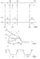
- FIG. 4 is a diagram indicating the potential variations across the pixel of the sensor shown on the right of FIG. 2 between the reservoir zone 19 and the substrate portion P located below the pinch zone 302.
- Three curves of potentials c1 , c2 and c3 are represented for each of the following operations: integration, read and reset.
- a dashed curve c represents the potential variations through this same pixel, directly above the source zone 24, passing through a "thick" portion of the buried layer N 30.
- the curve c is substantially identical regardless of the operation performed.
- the potential of the nip 302 varies little and is still well below the internal potential of a thick portion of the buried layer N 30. This potential difference is due to the fact that the nip 302 is completely depleted contrary to a thick portion of the buried layer N 30.
- Vdd voltage of the order of 3.3 V
- the potential value of the nip 302 is of the order of 1 V. The latter fluctuates slightly according to the operations performed.
- the potential in the reservoir zone 19, near the gate 20, is substantially zero.
- the potential then increases progressively through the reservoir zone 19 and the caisson 34 until it reaches a maximum value V1 in the middle of the nip 302.
- the potential then decreases progressively through the substrate portion P 36, between the nip 302 and the substrate 1.
- the potential of the upper P areas that is to say the reservoir zone 19 and the box 34, evolves as holes are stored.
- the potential of these upper P zones increases gradually with the arrival of holes.
- V1 of the pinch zone 302. it is possible for the potential of these upper P zones to reach the potential value V1 of the pinch zone 302.
- "excess" holes in the P zones higher are naturally directed to the substrate 1 by passing through the pinch zone 302. The number of holes stored is thus capped and the potential of the zones P exceeds the V1 value during an integration operation.
- the presence of a pinching zone in each pixel makes it possible to "cap” the potential of the reservoir zone and the box of this pixel to a value of potential substantially corresponding to the potential V1 of the pinch zone.
- This characteristic makes it possible to avoid "glare" phenomena, better known by their English name of "blooming", consisting of a disturbance of a read operation of a row of pixels due to an integration operation. simultaneous by other brightly lit pixels.
- the potential of the box P of a pixel in the integration phase can increase to a value of potential greater than the potential value present on the source line SL connected to this pixel, then the diode PN formed by the well P and the source zone of this pixel can become conductive and disturb the current reading operation.
- the potential in the reservoir zone 19, close to the gate 20 is equal to a value V2 greater than V1.
- the potential V2 is in this example equal to 2 V.
- the potential then decreases rapidly away from the gate 20 to reach a minimum in the box 34, of the order of 0.8 V in this example.
- the potential then rises gradually up to the nip 302 and then decreases again towards the substrate 1. Note that the stored holes are no longer confined near the grid but "accumulate" in the box 34.
- the potential in the reservoir zone 19, close to the gate 20, is substantially equal to the supply voltage Vdd, ie 3.3 V in this example.
- the potential then decreases progressively away from the grid. As a result, the holes previously stored in the reservoir zone 19 move towards the substrate 1.
- An advantage of a pixel according to the present invention is that low voltages, equal to the "standard" supply voltage of the sensor, can be used to evacuate holes accumulated under the gate of the transistor of the pixel.
- FIG. 5 is a diagram indicating the variations of potential across the boxes 33, 34 of the pixels of the sensor represented in FIG. 2.
- the represented potential curve corresponds to the potentials noted in the lower parts of the caissons 33, 34, located below the level of inter pixel isolation areas 27, 28 and 29.
- the curve shown corresponds to the potentials recorded during an integration operation, the source areas 15 and 25 being connected to the supply voltage Vdd.
- the potential in the portions of the caissons 33, 34 located above the nip zones 301 and 302 is low and close to 0 V in this example.
- the potential in the portions of the caissons 33, 34 located above the thick portions of the buried layer N is "high" and equal to V3, of the order of 2 V in this example.
- An advantage of a sensor according to the present invention is that the transistors of the sensor pixels can be separated from each other by shallow isolation areas.
- the isolation zones separating the pixels of the sensor may be identical to the "conventional" isolation zones separating "standard" transistors from the other blocks. of the integrated circuit.
- the potential of the lower parts of the boxes 33, 34 is mainly fixed by the capacitive couplings between these boxes and the buried layer N 30.
- the curve of the potentials in the lower parts of the boxes has a shape substantially identical to the potential curve through buried layer N 30.
- the potential in the lower part of a box further depends on the potentials applied to the elements of the transistor placed above.
- the potential of a source area can go from the voltage Vdd to a lower voltage and cause a slight drop in potential in the portion of the peripheral well below this source area.
- V3 at a potential value V4. If the potential value V4 is lower than the potential value V1, the holes stored in a pixel can migrate to the neighboring pixel.
- pinch areas prevent glare phenomena during read operations, use low voltages during reset operations, and isolate neighboring pixels.
- the surface of a nip 301, 302 in plan view is substantially identical to that of the channel region of the transistor placed above. However, this nip surface may be narrower or on the contrary more extensive. In general, the surface of a pinch zone should be large enough so that the capacitive influence of the pinch zone on the box placed above is significant and should not extend too far under the source zones. drain of the transistor placed above so that inter-pixel isolation is possible at the periphery of the pixel box.
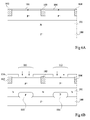
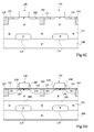
- FIG. 2 An image sensor such as that shown in FIG. 2 can be obtained for the method described hereinafter with reference to FIGS. 6A to 6D. It will be understood that various doped regions are illustrated as they appear after annealing steps which are not described.
- insulating zones 102, 103, 104 are formed in the upper part of a lightly doped substrate 100, for example of the P type.
- the insulating zones delimit portions. higher substrate constituting active areas of future transistors.
- An ion implantation of doping elements is then carried out in the substrate to form an N type doped buried layer 101.
- An ion implantation of doping elements is also carried out on the surface of the zones. active to form thin layers 105, 106 lightly doped P.
- a layer of photoresist 110 is deposited on the substrate 100.
- This resin is insulated and developed to form openings 111, 112 in the latter above central strips of the zones. active to form channel areas.
- An ion implantation of high energy doping elements is then carried out to form P type doped buried pockets 115, 116 in the lower part of the buried layer N 101, under the openings 111 and 112.
- the resin layer is then eliminated. 110.
- a thin dielectric layer constituted for example by silicon oxide
- a conductive layer for example made of polycrystalline silicon.
- These two layers are then etched so as to form transistor gates 120, 130 each constituted by a stack of an insulating portion and a conductive portion.
- An ion implantation of doping elements is then carried out in order to form source pre-zones 121, 131 and weakly doped N-type drain pre-zones 122, 132 on the surface of the substrate, on either side of the grids 120 , 130.
- insulating spacers 140, 150 are formed against the sidewalls of the grids 120, 130.
- An ion implantation of doping elements is then carried out in the upper part of the substrate to form zones of N-type doped source 141, 151 and drain 142, 152.
- the remaining portions of the layers P 105, 106 placed under the grids 120, 130 constitute reservoir zones 143, 153.
- the portions of the buried layer N 101 placed above the buried pockets 115, 116 are nips 160, 161.
- N-type access zones such as the access zone 32 of the sensor represented in FIG. 2, may be formed by ion implantation of doping elements in the substrate. 100. This implantation can be performed after the formation of the buried layer 101.
- the openings 111, 112 and consequently the buried bags P 115, 116 may be provided wider or on the contrary more restricted than the reservoir zones P 143, 153 placed under the grids 120 and 130.
- Such a pixel would comprise a P-channel transistor (PMOS) formed in and above an N-type substrate. comprising a buried P-type layer, P-type reservoir zones being formed under the gates of the transistors.
- PMOS P-channel transistor
Landscapes
- Solid State Image Pick-Up Elements (AREA)
- Transforming Light Signals Into Electric Signals (AREA)
Applications Claiming Priority (1)
| Application Number | Priority Date | Filing Date | Title |
|---|---|---|---|
| FR0650765 | 2006-03-06 |
Publications (1)
| Publication Number | Publication Date |
|---|---|
| EP1833092A1 true EP1833092A1 (de) | 2007-09-12 |
Family
ID=36599077
Family Applications (1)
| Application Number | Title | Priority Date | Filing Date |
|---|---|---|---|
| EP07103611A Withdrawn EP1833092A1 (de) | 2006-03-06 | 2007-03-06 | Bildsensor, der Pixel mit einem Transistor umfasst |
Country Status (2)
| Country | Link |
|---|---|
| US (1) | US7642579B2 (de) |
| EP (1) | EP1833092A1 (de) |
Cited By (1)
| Publication number | Priority date | Publication date | Assignee | Title |
|---|---|---|---|---|
| CN102709304A (zh) * | 2012-06-26 | 2012-10-03 | 天津大学 | 提高图像传感器满阱容量与量子效率光电二极管及方法 |
Citations (3)
| Publication number | Priority date | Publication date | Assignee | Title |
|---|---|---|---|---|
| US20020024071A1 (en) * | 2000-08-15 | 2002-02-28 | Innotech Corporation | Solid-state imaging device |
| JP2004187017A (ja) * | 2002-12-04 | 2004-07-02 | Innotech Corp | 読出処理装置 |
| US20050224844A1 (en) * | 2003-12-26 | 2005-10-13 | Akira Mizuguchi | Solid-state image sensing device |
Family Cites Families (3)
| Publication number | Priority date | Publication date | Assignee | Title |
|---|---|---|---|---|
| JP4065572B2 (ja) * | 1997-03-28 | 2008-03-26 | 株式会社ルネサステクノロジ | 半導体装置 |
| TW494574B (en) * | 1999-12-01 | 2002-07-11 | Innotech Corp | Solid state imaging device, method of manufacturing the same, and solid state imaging system |
| JP4004484B2 (ja) * | 2004-03-31 | 2007-11-07 | シャープ株式会社 | 固体撮像素子の製造方法 |
-
2007
- 2007-03-05 US US11/713,903 patent/US7642579B2/en active Active
- 2007-03-06 EP EP07103611A patent/EP1833092A1/de not_active Withdrawn
Patent Citations (3)
| Publication number | Priority date | Publication date | Assignee | Title |
|---|---|---|---|---|
| US20020024071A1 (en) * | 2000-08-15 | 2002-02-28 | Innotech Corporation | Solid-state imaging device |
| JP2004187017A (ja) * | 2002-12-04 | 2004-07-02 | Innotech Corp | 読出処理装置 |
| US20050224844A1 (en) * | 2003-12-26 | 2005-10-13 | Akira Mizuguchi | Solid-state image sensing device |
Non-Patent Citations (1)
| Title |
|---|
| PATENT ABSTRACTS OF JAPAN vol. 2003, no. 12 5 December 2003 (2003-12-05) * |
Cited By (1)
| Publication number | Priority date | Publication date | Assignee | Title |
|---|---|---|---|---|
| CN102709304A (zh) * | 2012-06-26 | 2012-10-03 | 天津大学 | 提高图像传感器满阱容量与量子效率光电二极管及方法 |
Also Published As
| Publication number | Publication date |
|---|---|
| US7642579B2 (en) | 2010-01-05 |
| US20070215909A1 (en) | 2007-09-20 |
Similar Documents
| Publication | Publication Date | Title |
|---|---|---|
| EP2216817B1 (de) | Von hinten beleuchteter halbleiter-bildsensor | |
| EP2587539B1 (de) | CMOS-UTBB-Bildaufnehmer | |
| EP3016141A1 (de) | Bilderfassungssensor mit vertikalen elektroden | |
| FR2930676A1 (fr) | Capteur d'image de tres faibles dimensions | |
| FR3019378A1 (fr) | Structure d'isolement entre des photodiodes | |
| FR2963187A1 (fr) | Dispositif d'imagerie a performances ameliorees et procede de commande. | |
| EP2415079A1 (de) | Selbstständige integrierte schaltung mit transistoren mit separaten schwellenspannungen | |
| FR2977982A1 (fr) | Matrice de photodiodes ingaas | |
| FR3043495A1 (fr) | Capteur d'images a obturation globale | |
| EP2685499A1 (de) | Integrierter SOI-Schaltkreis, der einen Triac zum Schutz gegen elektrostatische Entladungen umfasst | |
| JPWO2017126204A1 (ja) | 受光素子、受光素子の製造方法、撮像素子および電子機器 | |
| EP2355156A1 (de) | Fotodiode für Bildsensor | |
| FR2984607A1 (fr) | Capteur d'image a photodiode durcie | |
| FR3003691A1 (fr) | Finfet avec grille arriere | |
| FR2963163A1 (fr) | Procede de reinitialisation d'un photosite et photosite correspondant | |
| EP2312832B1 (de) | Pixelschaltung in Bildsensor | |
| US7420207B2 (en) | Photo-detecting device and related method of formation | |
| EP2685502A1 (de) | Integrierter SOI-Schaltkreis, der einen bipolaren Transistor mit Isolationsrinnen unterschiedlicher Tiefe umfasst | |
| EP3240030B1 (de) | Photodetektorgerät mit hochdotiertem interdioden-netz, und sein herstellungsverfahren | |
| EP1722421A2 (de) | Integrierte massefreie Fotodiode | |
| EP1722422A2 (de) | Integrierter Schaltkreis mit einer massefreien Fotodiode und Herstellungsverfahren dafür | |
| FR2934926A1 (fr) | Capteur d'images miniature. | |
| FR2911007A1 (fr) | Capteur d'image comprenant des pixels a un transistor | |
| EP1833092A1 (de) | Bildsensor, der Pixel mit einem Transistor umfasst | |
| JP2025077004A (ja) | イメージセンサー |
Legal Events
| Date | Code | Title | Description |
|---|---|---|---|
| PUAI | Public reference made under article 153(3) epc to a published international application that has entered the european phase |
Free format text: ORIGINAL CODE: 0009012 |
|
| AK | Designated contracting states |
Kind code of ref document: A1 Designated state(s): AT BE BG CH CY CZ DE DK EE ES FI FR GB GR HU IE IS IT LI LT LU LV MC MT NL PL PT RO SE SI SK TR |
|
| AX | Request for extension of the european patent |
Extension state: AL BA HR MK YU |
|
| 17P | Request for examination filed |
Effective date: 20080312 |
|
| AKX | Designation fees paid |
Designated state(s): DE FR GB IT |
|
| 17Q | First examination report despatched |
Effective date: 20080502 |
|
| STAA | Information on the status of an ep patent application or granted ep patent |
Free format text: STATUS: THE APPLICATION IS DEEMED TO BE WITHDRAWN |
|
| 18D | Application deemed to be withdrawn |
Effective date: 20121001 |