EP1833096A1 - Auf cis basierende dünnfilm-solarbatterie und herstellungsprozess dafür - Google Patents
Auf cis basierende dünnfilm-solarbatterie und herstellungsprozess dafür Download PDFInfo
- Publication number
- EP1833096A1 EP1833096A1 EP05814238A EP05814238A EP1833096A1 EP 1833096 A1 EP1833096 A1 EP 1833096A1 EP 05814238 A EP05814238 A EP 05814238A EP 05814238 A EP05814238 A EP 05814238A EP 1833096 A1 EP1833096 A1 EP 1833096A1
- Authority
- EP
- European Patent Office
- Prior art keywords
- layer
- alkali
- back electrode
- electrode layer
- metallic back
- Prior art date
- Legal status (The legal status is an assumption and is not a legal conclusion. Google has not performed a legal analysis and makes no representation as to the accuracy of the status listed.)
- Withdrawn
Links
Images




Classifications
-
- H—ELECTRICITY
- H10—SEMICONDUCTOR DEVICES; ELECTRIC SOLID-STATE DEVICES NOT OTHERWISE PROVIDED FOR
- H10F—INORGANIC SEMICONDUCTOR DEVICES SENSITIVE TO INFRARED RADIATION, LIGHT, ELECTROMAGNETIC RADIATION OF SHORTER WAVELENGTH OR CORPUSCULAR RADIATION
- H10F77/00—Constructional details of devices covered by this subclass
- H10F77/10—Semiconductor bodies
- H10F77/12—Active materials
- H10F77/126—Active materials comprising only Group I-III-VI chalcopyrite materials, e.g. CuInSe2, CuGaSe2 or CuInGaSe2 [CIGS]
-
- H—ELECTRICITY
- H10—SEMICONDUCTOR DEVICES; ELECTRIC SOLID-STATE DEVICES NOT OTHERWISE PROVIDED FOR
- H10F—INORGANIC SEMICONDUCTOR DEVICES SENSITIVE TO INFRARED RADIATION, LIGHT, ELECTROMAGNETIC RADIATION OF SHORTER WAVELENGTH OR CORPUSCULAR RADIATION
- H10F10/00—Individual photovoltaic cells, e.g. solar cells
- H10F10/10—Individual photovoltaic cells, e.g. solar cells having potential barriers
- H10F10/16—Photovoltaic cells having only PN heterojunction potential barriers
- H10F10/167—Photovoltaic cells having only PN heterojunction potential barriers comprising Group I-III-VI materials, e.g. CdS/CuInSe2 [CIS] heterojunction photovoltaic cells
-
- H—ELECTRICITY
- H10—SEMICONDUCTOR DEVICES; ELECTRIC SOLID-STATE DEVICES NOT OTHERWISE PROVIDED FOR
- H10F—INORGANIC SEMICONDUCTOR DEVICES SENSITIVE TO INFRARED RADIATION, LIGHT, ELECTROMAGNETIC RADIATION OF SHORTER WAVELENGTH OR CORPUSCULAR RADIATION
- H10F19/00—Integrated devices, or assemblies of multiple devices, comprising at least one photovoltaic cell covered by group H10F10/00, e.g. photovoltaic modules
- H10F19/30—Integrated devices, or assemblies of multiple devices, comprising at least one photovoltaic cell covered by group H10F10/00, e.g. photovoltaic modules comprising thin-film photovoltaic cells
-
- H—ELECTRICITY
- H10—SEMICONDUCTOR DEVICES; ELECTRIC SOLID-STATE DEVICES NOT OTHERWISE PROVIDED FOR
- H10F—INORGANIC SEMICONDUCTOR DEVICES SENSITIVE TO INFRARED RADIATION, LIGHT, ELECTROMAGNETIC RADIATION OF SHORTER WAVELENGTH OR CORPUSCULAR RADIATION
- H10F77/00—Constructional details of devices covered by this subclass
- H10F77/10—Semiconductor bodies
- H10F77/16—Material structures, e.g. crystalline structures, film structures or crystal plane orientations
- H10F77/169—Thin semiconductor films on metallic or insulating substrates
- H10F77/1694—Thin semiconductor films on metallic or insulating substrates the films including Group I-III-VI materials, e.g. CIS or CIGS
-
- H—ELECTRICITY
- H10—SEMICONDUCTOR DEVICES; ELECTRIC SOLID-STATE DEVICES NOT OTHERWISE PROVIDED FOR
- H10F—INORGANIC SEMICONDUCTOR DEVICES SENSITIVE TO INFRARED RADIATION, LIGHT, ELECTROMAGNETIC RADIATION OF SHORTER WAVELENGTH OR CORPUSCULAR RADIATION
- H10F77/00—Constructional details of devices covered by this subclass
- H10F77/20—Electrodes
- H10F77/206—Electrodes for devices having potential barriers
- H10F77/211—Electrodes for devices having potential barriers for photovoltaic cells
-
- Y—GENERAL TAGGING OF NEW TECHNOLOGICAL DEVELOPMENTS; GENERAL TAGGING OF CROSS-SECTIONAL TECHNOLOGIES SPANNING OVER SEVERAL SECTIONS OF THE IPC; TECHNICAL SUBJECTS COVERED BY FORMER USPC CROSS-REFERENCE ART COLLECTIONS [XRACs] AND DIGESTS
- Y02—TECHNOLOGIES OR APPLICATIONS FOR MITIGATION OR ADAPTATION AGAINST CLIMATE CHANGE
- Y02E—REDUCTION OF GREENHOUSE GAS [GHG] EMISSIONS, RELATED TO ENERGY GENERATION, TRANSMISSION OR DISTRIBUTION
- Y02E10/00—Energy generation through renewable energy sources
- Y02E10/50—Photovoltaic [PV] energy
- Y02E10/541—CuInSe2 material PV cells
-
- Y—GENERAL TAGGING OF NEW TECHNOLOGICAL DEVELOPMENTS; GENERAL TAGGING OF CROSS-SECTIONAL TECHNOLOGIES SPANNING OVER SEVERAL SECTIONS OF THE IPC; TECHNICAL SUBJECTS COVERED BY FORMER USPC CROSS-REFERENCE ART COLLECTIONS [XRACs] AND DIGESTS
- Y02—TECHNOLOGIES OR APPLICATIONS FOR MITIGATION OR ADAPTATION AGAINST CLIMATE CHANGE
- Y02P—CLIMATE CHANGE MITIGATION TECHNOLOGIES IN THE PRODUCTION OR PROCESSING OF GOODS
- Y02P70/00—Climate change mitigation technologies in the production process for final industrial or consumer products
- Y02P70/50—Manufacturing or production processes characterised by the final manufactured product
Definitions
- the present invention relates to an alkali-barrier layer of a CIS type thin-film solar cell (the alkali-barrier layer, when a light absorption layer is deposited on a metallic back electrode layer, blocks and controls the diffusion of alkali ingredients from the glass substrate underlying the metallic back electrode layer) and to a process for forming the layer.
- the invention relates to a CIS type thin-film solar cell having a pn heterojunction comprising: a p-type semiconductor such as a thin multinary-compound semiconductor film, in particular, a I-III-VI 2 Group chalcopyrite semiconductor, e.g., copper indium diselenide (CuInSe 2 ), copper indium gallium diselenide (CuInGaSe 2 ), copper gallium diselenide (CuGaSe 2 ), copper indium gallium di-sulfo-sulfide (Cu (InGa) (SSe) 2 ), copper indium disulfide (CuInS 2 ), copper gallium disulfide (CuGaS 2 ), copper indium gallium disulfide (CuInGaS 2 ), or copper indium gallium diselenide (CuInGaSe 2 ) having a thin film of copper indium gallium di-sulfo-sulfide (Cu(InGa)(SSe) 2
- a CIS type thin-film solar cell 1B heretofore in use has a basic structure such as that shown in Fig. 7. It is a pn heterojunction device having a substrate structure comprising a substrate 2 comprising a soda-lime float glass and, superposed thereon in the following order, high-quality thin layers composed of a metallic back electrode layer (generally molybdenum) 3, a p-type CIS-based light absorption layer 4, a high-resistance buffer layer 5, and an n-type window layer (transparent conductive film) 6.
- a soda-lime float glass is employed as the substrate 2 because it is inexpensive.
- alkali ingredients e.g., Na, Ca, Mg, and K
- these alkali ingredients thermally diffuse into the light absorption layer excessively, the light absorption layer 4 peels off at the interface of the metallic back electrode layer.
- sodium which has deliquescence, comes to be unevenly contained in the light absorption layer, this is a cause of instability or a reduced life of the light absorption layer itself, etc.
- an alkali-barrier layer made of an oxide, nitride, or the like is deposited.
- Second investigations which have been published are ones in which influences of the deposition of an alkali-barrier layer on solar cell characteristics are discussed; while second investigations which have been published are ones employing a production process which comprises purposely depositing an alkali-barrier layer capable of completely preventing the diffusion of alkali ingredients from a soda-lime float glass substrate, depositing a metallic back electrode layer on the alkali-barrier layer, and separately further depositing a layer containing a necessary amount of sodium to produce a solar cell.
- the second investigations are ones which comprise purposely depositing an alkali-barrier layer capable of completely preventing the diffusion of alkali ingredients from a soda-lime float glass substrate, depositing a metallic back electrode layer thereon, and separately further depositing a layer containing a necessary amount of sodium (see, for example, non-patent documents 3, 4, and 5).
- the alkali-barrier layers of the CIS type thin-film solar cells in the investigations which have been published so far are independent ultrathin layers made of, e.g., an oxide or a nitride.
- an object of the invention is to provide a production process by which an alkali-barrier layer capable of controlling the amount of alkali ingredients to be diffused and necessary for forming a high-quality light absorption layer is formed with high reproducibility, in order to improve solar cell performances (e.g., conversion efficiency and open-circuit voltage).
- Another object of the invention is to provide a production process in which alkali ingredient diffusion from a soda-lime float glass substrate can be secured in an amount necessary for forming a CIS-based light absorption layer having device characteristics capable of attaining a high conversion efficiency.
- Still another object of the invention is to provide a production process which eliminates the necessity of a production process comprising the step of depositing an alkali-barrier layer capable of completely preventing the diffusion of alkali ingredients from a soda-lime float glass substrate and the step of depositing a sodium-containing layer.
- the related-art deposition of a thin layer of an oxide, nitride, or the like by the RF sputtering method using a ceramic target, e.g., an oxide or a nitride has a low deposition rate.
- a ceramic target e.g., an oxide or a nitride
- deposition pressure regulation therein is difficult and there has hence been a problem that it is difficult to optimize each of the thin layer of an oxide, a nitride, or the like and the metallic back electrode layer.
- a further object of the invention is to provide a production process in which a thin layer of an oxide, a nitride, or the like and a metallic back electrode layer can be successively deposited in the same sputtering apparatus at a constant substrate conveyer speed or rotation speed.
- B boron
- a further object of the invention is to provide a production process which is free from the risk of causing an increase in resistance due to the oxidation of the metallic back electrode layer and does not increase the apparatus cost and in which a high-quality alkali-barrier layer and a high-quality metallic back electrode layer are successively deposited in the same sputtering apparatus at a constant substrate conveyer speed.
- the invention which eliminates the problems described above, provides a CIS type thin-film solar cell which is a pn heterojunction device having a substrate structure comprising a glass substrate, an alkali-free layer, a multilayered metallic back electrode layer, a p-type CIS-based light absorption layer, a high-resistance buffer layer, and an n-type window layer which have been superposed in this order, wherein the alkali-free layer has an alkali-barrier function for preventing and controlling the thermal diffusion of alkali ingredients from the glass substrate into the light absorption layer when the light absorption layer is deposited.
- the invention provides a CIS type thin-film solar cell which is a pn heterojunction device having a substrate structure comprising a glass substrate, an alkali-free layer, a multilayered metallic back electrode layer, a p-type CIS-based light absorption layer, a high-resistance buffer layer, and an n-type window layer which have been superposed in this order, wherein the alkali-free layer and the first layer of the multilayered metallic back electrode layer have an alkali-barrier function for preventing and controlling the thermal diffusion of alkali ingredients from the glass substrate into the light absorption layer when the light absorption layer is deposited.
- the invention provides the CIS type thin-film solar cell as described under (1) or (2) above, wherein the alkali-free layer comprises an oxide or a nitride.
- the invention provides the CIS type thin-film solar cell as described under (1), (2), or (3) above, wherein the alkali-free layer comprises an oxide, a nitride, or a special compound, and desirably comprises silica (SiO 2 or SiO 2-x ).
- the invention provides the CIS type thin-film solar cell as described under any one of (1) to (4) above, wherein the alkali-free layer comprises silica having the stoichiometric composition (SiO 2 ) and/or silica which does not have the stoichiometric composition and tends to be somewhat deficient in oxygen (SiO 2-x ).
- the invention provides the CIS type thin-film solar cell as described under any one of (1) to (5) above, wherein the alkali-free layer has a thickness in the range of 3-100 nm, desirably 20-50 nm.
- the invention provides the CIS type thin-film solar cell as described under (2) above, wherein the first layer of the metallic back electrode layer comprises crystal grains of the metal which are fine grains having a high density and having a regulated crystal grain diameter.
- the invention provides the CIS type thin-film solar cell as described under (2) above, wherein the total thickness of the alkali-free layer and the first layer of the metallic back electrode layer is 50-110 nm.
- the invention provides the CIS type thin-film solar cell as described under (1) or (2) above, wherein the multilayered metallic back electrode layer comprises Mo (molybdenum) and has a multilayer structure composed of two or more layers.
- the invention provides the CIS type thin-film solar cell as described under (1), (2), or (9) above, wherein the multilayered metallic back electrode layer has a thickness in the range of 100-1,000 nm, desirably in the range of 300-500 nm.
- the invention provides a process for producing a CIS type thin-film solar cell which is a pn heterojunction device having a substrate structure comprising a glass substrate, an alkali-free layer, a multilayered metallic back electrode layer, a p-type CIS-based light absorption layer, a high-resistance buffer layer, and an n-type window layer which have been superposed in this order, wherein the alkali-free layer and the multilayered metallic back electrode layer directly overlying the alkali-free layer are formed by a method which comprises depositing the alkali-free layer on the glass substrate, thereafter depositing the multilayered metallic back electrode layer on the alkali-free layer, and imparting to the alkali-free layer an alkali-barrier function for preventing and controlling the thermal diffusion of alkali ingredients from the glass substrate into the light absorption layer when the light absorption layer is deposited.
- the invention provides a process for producing a CIS type thin-film solar cell which is a pn heterojunction device having a substrate structure comprising a glass substrate, an alkali-free layer, a multilayered metallic back electrode layer, a p-type CIS-based light absorption layer, a high-resistance buffer layer, and an n-type window layer which have been superposed in this order, wherein the alkali-free layer and the multilayered metallic back electrode layer are formed by a method which comprises depositing the alkali-free layer on the glass substrate, thereafter depositing the multilayered metallic back electrode layer on the alkali-free layer using changed deposition conditions in depositing the first layer of the multilayered metallic back electrode layer to thereby regulate the crystal grain diameter thereof, and imparting to the alkali-free layer and the first layer of the metallic back electrode layer an alkali-barrier function for preventing and controlling the thermal diffusion of alkali ingredients from the glass substrate into the light absorption layer when the light absorption layer is deposited.
- the invention provides the process for producing a CIS type thin-film solar cell as described under (11) or (12) above, wherein the alkali-free layer is deposited by the RF sputtering method in an inert gas, e. g., argon gas, using a silica target or by the reactive DC sputtering method in a gaseous mixture of argon gas and oxygen using one or more silicon metal targets alloyed with a metallic element, e.g., boron, for imparting conductivity to metallic silicon.
- an inert gas e. g., argon gas
- the invention provides the process for producing a CIS type thin-film solar cell as described under (11) or (12) above, wherein the electric power to be applied to the target (s) during the deposition of the alkali-free layer by sputtering is in the range of 0.5-1.5 Watt/cm 2 in the RF sputtering method and is in the range of 1.0-3.0 Watt/cm 2 in the DC sputtering method, and the electric power is determined so that the first layer of the metallic back electrode layer comprises crystal grains which are fine grains having a grain diameter (grain size) of 10 nm or smaller, desirably in the range of 3-5 nm.
- the electric power to be applied to the target (s) during the deposition of the alkali-free layer by sputtering is in the range of 0.5-1.5 Watt/cm 2 in the RF sputtering method and is in the range of 1.0-3.0 Watt/cm 2 in the DC sputtering method, and the electric power is determined so
- the invention provides the process for producing a CIS type thin-film solar cell as described under (11) or (12) above, wherein the deposition pressure during the deposition of the alkali-free layer by sputtering is in the range of 0.5-5 Pa (pascals), desirably in the range of 0.5-1.5 Pa (pascals), and the deposition pressure is determined so that the first layer of the metallic back electrode layer comprises fine grains having a grain diameter in the range of 3-5 nm.
- the invention provides the process for producing a CIS type thin-film solar cell as described under (11) or (12) above, wherein the electric power to be applied to the target during the deposition of the first layer of the multilayered metallic back electrode layer by sputtering is in the range of from 1/8 to 1/2 of the electric power to be applied to the target during the deposition by sputtering of the metallic back electrode layer directly overlying the first layer, and by thus regulating the voltage to be applied to the target, the first layer is made to comprise fine grains having a grain diameter of 10 nm or smaller, desirably 3-5 nm, and having a high density.
- the invention provides the process for producing a CIS type thin-film solar cell as described under (11) or (12) above, wherein the multilayered metallic back electrode layer is continuously deposited at a constant substrate conveyer speed.
- the invention provides the process for producing a CIS type thin-film solar cell as described under (11) or (12) above, wherein the multilayered metallic back electrode layer is deposited by the DC sputtering method in an argon gas as an inert gas using a metal (e.g., molybdenum (Mo)) as a target.
- a metal e.g., molybdenum (Mo)
- the invention provides the process for producing a CIS type thin-film solar cell as described under (11) or (12) above, wherein the multilayered metallic back electrode layer comprises any one refractory metal selected from metals having resistance to selenium, such as molybdenum (Mo), titanium (Ti), and tantalum (Ta), or a combination thereof resulting from the formation of a compound (e.g., MoSiO x , etc.) with the silica layer.
- Mo molybdenum
- Ti titanium
- Ta tantalum
- the invention provides the process for producing a CIS type thin-film solar cell as described under (11) or (12) above, wherein a pressure regulation mechanism and/or an independent vacuum system is disposed between an alkali-free-layer deposition chamber for depositing the alkali-free layer and a metallic-back-electrode layer deposition chamber for depositing the metallic back electrode layer and the two thin layers are deposited in respective sputtering gas atmospheres (e.g., argon gas, Ar+O 2 mixture gas) differing in pressure and/or composition.
- sputtering gas atmospheres e.g., argon gas, Ar+O 2 mixture gas
- a metallic back electrode layer can be successively deposited in the same sputtering apparatus and the excess thermal diffusion of alkali ingredients into the light absorption layer can be prevented and controlled.
- the light absorption layer can be prevented from peeling off at the interface of the metallic back electrode layer without reducing solar cell performances (conversion efficiency and open-circuit voltage).
- conversion efficiency and open-circuit voltage conversion efficiency and open-circuit voltage
- the invention is applicable to a ceramic target which is an oxide or nitride having no electrical conductivity.
- two or more deposition steps for depositing different materials can be conducted in the same in-line type sputtering apparatus by depositing a silica layer using a silica target attaining high insulating properties by the RF sputtering method, which has a low deposition rate because a high power cannot be applied, and depositing the first layer of a multilayered metallic back electrode layer successively to the silica layer deposition by the DC sputtering method, in which the deposition rate can be improved by increasing the power to be applied, at the same deposition pressure and the same substrate conveyer speed.
- the invention can eliminate the problems associated with differences in deposition conditions between two different sputtering methods to thereby enable film deposition to be conducted at the same substrate conveyance speed.
- a two-layer structure can be formed by depositing a silica layer by the RF sputtering method and successively depositing the first layer of amultilayeredmetallic back electrode layer by the DC sputtering method.
- the invention can contribute to a reduction of the cost of a CIS type thin-film solar cell.
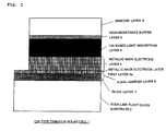
- the invention relates to a method of forming an alkali-barrier layer 8 for preventing and controlling the thermal diffusion of alkali ingredients from a soda-lime float glass substrate 2 into a light absorption layer 4 comprising a p-type semiconductor when the light absorption layer is deposited on a metallic back electrode layer 3 deposited on the soda-lime float glass substrate 2.
- the invention further relates to a CIS type thin-film solar cell 1 having the alkali-barrier layer 8.
- This alkali-barrier layer 8 may be a first alkali-barrier layer which is a silica layer 7 formed on the soda-lime float glass substrate, or may be a second alkali-barrier layer which is a multilayered alkali-barrier layer composed of the silica layer 7 and the first layer 3a of the multilayered metallic back electrode layer directly overlying the silica layer 7.
- the CIS type thin-film solar cell 1 of the invention has a basic structure such as that shown in Fig. 7. It is a pn heterojunction device having a substrate structure comprising a substrate 2 comprising a soda-lime float glass and, superposed thereon in the following order, high-quality thin layers composed of a metallic back electrode layer (generally molybdenum) 3, a p-type CIS-based light absorption layer 4, a high-resistance buffer layer 5, and an n-type window layer (transparent conductive film) 6.
- a metallic back electrode layer generally molybdenum
- a p-type CIS-based light absorption layer 4 a high-resistance buffer layer
- an n-type window layer transparent conductive film
- the light absorption layer 4 comprises a p-type semiconductor such as a thin multinary-compound semiconductor film, in particular, aI-III-VI 2 Group chalcopyrite semiconductor, e.g., copper indium diselenide (CuInSe 2 ), copper indium gallium diselenide (CuInGaSe 2 ), copper gallium diselenide (CuGaSe 2 ), copper indium gallium disulfo-selenide (Cu(InGa) (SSe) 2 ), copper indium disulfide (CuInS 2 ), copper gallium disulfide (CuGaS 2 ) , copper indium gallium disulfide (CuInGaS 2 ), or copper indium gallium diselenide (CuInGaSe 2 ) having a thin film of copper indium gallium disulfo-selenide (Cu(InGa) (SSe) 2 ) as a surface layer.
- a soda-lime float glass is employed as the substrate 2 because it is inexpensive.
- alkali ingredients e.g., Na, Ca, Mg, and K
- these alkali ingredients thermally diffuse into the light absorption layer excessively, the light absorption layer 4 peels off at the interface of the metallic back electrode layer.
- sodium, which has deliquescence comes to be unevenly contained in the light absorption layer, this is a cause of instability or a reduced life of the light absorption layer itself, etc.
- an alkali-barrier layer 8 as shown in Fig. 1, for preventing and controlling the thermal diffusion of alkali ingredients from a soda-lime float glass substrate 2 into a light absorption layer comprising a p-type semiconductor when the light absorption layer 4 is deposited on a metallic back electrode layer 3 deposited on the soda-lime float glass substrate 2.
- the alkali-barrier layer 8 may be: a first alkali-barrier layer which consists only of an alkali-free silica layer 7 formed on the soda-lime float glass substrate; or a second alkali-barrier layer which is a multilayered alkali barrier layer composed of the silica layer 7 and the first layer 3A of the multilayeredmetallic back electrode layer directly overlying the silica layer 7, the first layer 3A having a regulated crystal grain diameter.
- the metallic back electrode layer 3 has a multilayer structure composed of two or more layers. A metallic back electrode layer 3 having a single-layer structure may be employed although this results in a slight decrease in the effect of peeling resistance.
- the alkali-free layer 7 comprises an oxide, a nitride, or a special compound, and desirably comprises silica.
- silica having the stoichiometric composition (SiO 2 ) and/or silica which does not have the stoichiometric composition and tends to be somewhat deficient in oxygen (SiO 2-x ) is suitable.
- the thickness of the alkali-free (silica) layer may be in the range of 3-100 nm, desirably 20-50 nm.
- the multilayered metallic back electrode layer 3 may have a multilayer structure composed of three or more layers, and may be made of Mo (molybdenum).
- the first layer 3a of the metallic back electrode layer 3 may comprise crystal grains of the metal which are fine grains and have a high density.
- the thickness thereof may be in the range of 10-100 nm, desirably 30-60 nm.
- the thickness of the multilayered metallic back electrode layer 3 may be in the range of 100-1,000 nm, desirably in the range of 300-500 nm.
- a silica layer 7 which is alkali-free is deposited in an RF sputtering part B either by the RF sputtering method using an alkali-free stable silica target or by the reactive DC sputtering method in an Ar+O 2 mixed gas atmosphere using an Si-B alloy target which is an alloy with boron or the like for improving electrical conductivity.
- film deposition is conducted in a DC sputtering part D in the same sputtering apparatus by the DC sputtering method, in which an increased deposition rate can be used.
- film deposition is conducted in DC sputtering parts D1, D2, D3, and D4 at the same deposition pressure and the same substrate conveyer speed using argon gas as a sputtering gas to form a multilayered metallic back electrode layer 3.
- an alkali-barrier layer is formed which has high quality and a necessary thickness and has a two-layer structure composed of the silica layer 7 and that first layer 3a of the metallic back electrode layer which has been formed while regulating the power being applied.
- a pressure regulation mechanism C may be disposed between the RF sputtering part (alkali-free-layer deposition chamber) for depositing the silica layer 7 and the DC sputtering part D (metallic-back-electrode layer deposition chamber) for depositing the metallic back electrode layer 3, whereby the two thin layers can be formed respectively using different pressures and different sputtering gas compositions (e.g., Ar+O 2 mixed gas in the reactive DC sputtering method).
- the deposition of a silica layer 7 is specifically as follows.
- One or more silica targets are used to deposit the film by the RF sputtering method in an inert gas (argon gas).
- one or more silicon metal targets alloyed with a metallic element, e.g., boron, for imparting conductivity to metallic silicon are used to deposit the film by the reactive DC sputtering method in a gaseous mixture of argon gas and oxygen.
- the electric power to be applied to the target(s) during the deposition by sputtering maybe in the range of 0.5-1.5 Watt/cm 2 in the RF sputtering method and may be in the range of 1.0-3.0 Watt/cm 2 in the DC sputtering method.
- the electric power to be applied may be determined so as to result in fine crystal grains having a diameter of 10 nm or smaller, desirably in the range of 3-5 nm.
- the deposition pressure during the deposition of the silica layer 7 by sputtering may be regulated to a value in the range of 0.5-5 Pa (pascals), desirably in the range of 0.5-1.5 Pa (pascals), so as to result in fine grains having a grain diameter in the range of 3-5 nm.
- the multilayered metallic back electrode layer is continuously deposited by the DC sputtering method at a constant substrate conveyer speed or rotation speed.
- any one refractory metal selected from metals having resistance to selenium, such as molybdenum (Mo), titanium (Ti), and tantalum (Ta), or metals comprising a combination of any of these (e.g., molybdenum (Mo)) resulting from the formation of a crystalline structure (e.g., MoSiO x , etc.) with the silica layer are used as a target to deposit the metallic back electrode layer by the DC sputtering method in an argon gas as an inert gas.
- the voltage to be applied to the target is regulated to thereby form crystal grains of the metal which are fine grains and have a high density.
- the electric power to be applied to the target during the deposition by sputtering may be in the range of from 1/8 to 1/2 of the electric power to be applied to the target during the deposition by sputtering of the metallic back electrode layer 3 directly overlying the first layer, and may be determined so as to result in a crystal grain diameter of 10 nm or smaller, desirably in the range of 3-5 nm.
- the deposition pressure during the deposition by sputtering may be in the range of 0.5-1.5 Pa (pascals) and determined so as to result in a grain diameter of 10 nm or smaller, desirably in the range of 3-5 nm.
- CIS type thin-film solar cell 1 of the invention which have an alkali-barrier layer
- Table 1 given below shows a comparison in performance between the CIS type thin-film solar cells 1A of the invention, which have an alkali-barrier layer, and a related-art CIS type thin-film solar cell 1B having no alkali-barrier layer.
- CIS type thin-film solar cell of the invention having a silica layer only; no first layer in the metallic back electrode layer ⁇ Round spots of different color are found on the surface of a metallic back electrode layer.
- CIS type thin-film solar cell of the invention ⁇ CIS-based light absorption layer does not peel off at the interface of a metallic back electrode having an alkali-barrier layer layer. (having a silica layer and the first layer in metallic back electrode layer) ⁇ Round spots of different color are found slightly on the surface of a metallic back electrode layer, but the surface of the metallic back electrode layer as a whole is fine.
- alkali ingredients are thermally diffused excessively into the light absorption layer and this CIS-based light absorption layer has poor adhesion to the metallic back electrode layer and peels off at the interface between the light absorption layer and the metallic back electrode layer.
- the metallic back electrode layer does not have the first layer, the light absorption layer has poor adhesion to the metallic back electrode layer and peels off at the interface between the light absorption layer and the metallic back electrode layer.
- the metallic back electrode layer does not peel off at the interface of the glass substrate. In this case, however, a phenomenon occurs in which the CIS-based light absorption layer peels off at the interface of the metallic back electrode layer to form round spots of a different color in the surface of the metallic back electrode layer.
- this solar cell is free from the peeling of the metallic back electrode layer from the glass substrate and the peeling of the CIS-based light absorption layer from the metallic back electrode layer, and the round spots of a different color on the surface of the metallic back electrode layer are considerably diminished.
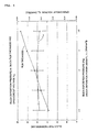
- FIG. 3 An example of conditions for forming a silica layer (silica layer deposition pressure) in the alkali-barrier layer according to the invention is shown in Fig. 3.
- the figure shows changes of the thickness of the silica layer deposited and changes of the open-circuit voltage (Volt/cell) of a CIS type thin-film solar cell having this silica layer with changes in silica deposition pressure (Pa) in silica deposition at a constant applied power (power density) of 1.0 Watt/cm 2 .
- the silica deposition pressure (Pa) increases, the silica film thickness increases.
- the open-circuit voltage is almost constant.
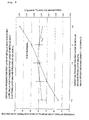
- FIG. 4 An example of conditions for forming a silica layer (sputtering power to be applied for silica layer deposition) in the alkali-barrier layer according to the invention is shown in Fig. 4.
- the figure shows changes of the thickness of the silica layer deposited and changes of the open-circuit voltage (Volt/cell) of a CIS type thin-film solar cell having this silica layer with changes in silica layer deposition power density (Watt/cm 2 ).
- the silica deposition power density (w/cm 2 ) increases, the silica film thickness increases.
- the open-circuit voltage is almost constant.
- FIG. 5 An example of conditions for forming the first layer of a metallic back electrode layer (deposition pressure for the first layer of metallic back electrode layer) in the alkali-barrier layer according to the invention is shown in Fig. 5.
- Silica layer deposition was conducted at a deposition power density of 1.55 (Watt/cm 2 ) and the first layer of a metallic back electrode layer was formed while changing the deposition pressure (Pa) among deposition conditions.
- the figure shows changes of the thickness of the first layer of the metallic back electrode layer deposited and changes of the open-circuit voltage (Volt/cell) of a CIS type thin-film solar cell having the silica layer and first layer of the metallic back electrode layer deposited under those conditions, with changes in the deposition pressure (Pa).
- the deposition pressure (Pa) increases, the thickness of the first layer of the metallic back electrode layer increases.
- the open-circuit voltage of the CIS type thin-film solar cell is almost constant.
- FIG. 6 An example of conditions for forming the first layer of a metallic back electrode layer (sputtering power to be applied for the first layer of the metallic back electrode layer) in the alkali-barrier layer according to the invention is shown in Fig. 6.
- Silica layer deposition was conducted at a deposition power density of 1.55 (Watt/cm 2 ) and the first layer of a metallic back electrode layer was formed while changing the power density (Watt/cm 2 ) among deposition conditions.
- the figure shows changes of the thickness of the first layer of the metallic back electrode layer and changes of the open-circuit voltage (Volt/cell) of a CIS type thin-film solar cell having the silica layer and the first layer of the metallic back electrode layer deposited under those conditions, with changes in the power density (Watt/cm 2 ) .
- the power density (Watt/cm 2 ) increases, the thickness of the first layer of the metallic back electrode layer increases.
- the open-circuit voltage of the CIS type thin-film solar cell is almost constant.
Landscapes
- Photovoltaic Devices (AREA)
Applications Claiming Priority (2)
| Application Number | Priority Date | Filing Date | Title |
|---|---|---|---|
| JP2004356909A JP2006165386A (ja) | 2004-12-09 | 2004-12-09 | Cis系薄膜太陽電池及びその作製方法 |
| PCT/JP2005/022698 WO2006062206A1 (ja) | 2004-12-09 | 2005-12-09 | Cis系薄膜太陽電池及びその作製方法 |
Publications (2)
| Publication Number | Publication Date |
|---|---|
| EP1833096A1 true EP1833096A1 (de) | 2007-09-12 |
| EP1833096A4 EP1833096A4 (de) | 2014-10-01 |
Family
ID=36578026
Family Applications (1)
| Application Number | Title | Priority Date | Filing Date |
|---|---|---|---|
| EP05814238.1A Withdrawn EP1833096A4 (de) | 2004-12-09 | 2005-12-09 | Auf cis basierende dünnfilm-solarbatterie und herstellungsprozess dafür |
Country Status (6)
| Country | Link |
|---|---|
| US (1) | US20080271781A1 (de) |
| EP (1) | EP1833096A4 (de) |
| JP (1) | JP2006165386A (de) |
| KR (1) | KR20070100249A (de) |
| CN (1) | CN101076895B (de) |
| WO (1) | WO2006062206A1 (de) |
Cited By (12)
| Publication number | Priority date | Publication date | Assignee | Title |
|---|---|---|---|---|
| WO2009041758A1 (en) * | 2007-09-28 | 2009-04-02 | Korea Reserach Institute Of Chemical Thchnology | Preparation method of chalcopyrite-type compounds with microwave irradiation |
| FR2922046A1 (fr) * | 2007-10-05 | 2009-04-10 | Saint Gobain | Perfectionnements apportes a des elements capables de collecter de la lumiere |
| WO2009144086A1 (fr) | 2008-04-16 | 2009-12-03 | Agc Flat Glass Europe Sa | Substrat en verre portant une electrode |
| WO2013149756A1 (de) * | 2012-04-02 | 2013-10-10 | Robert Bosch Gmbh | Mehrschicht-rückelektrode für eine photovoltaische dünnschichtsolarzelle und verwendung der selben für die herstellung von dünnschichtsolarzellen und -modulen, photovoltaische dünnschichtsolarzellen und -module enthaltend die mehrschicht-rückelektrode sowie ein verfahren zu deren herstellung |
| WO2013149757A1 (de) * | 2012-04-02 | 2013-10-10 | Robert Bosch Gmbh | Mehrschicht-rückelektrode für eine photovoltaische dünnschichtsolarzelle, verwendung derselben für die herstellung von dünnschichtsolarzellen und -modulen, photovoltaische dünnschichtsolarzellen und -module enthaltend die mehrschicht-rückelektrode sowie ein herstellungsverfahren |
| EP2443660A4 (de) * | 2009-06-16 | 2014-03-26 | Lg Innotek Co Ltd | Solarzelle und herstellungsverfahren dafür |
| EP2280419A4 (de) * | 2008-05-19 | 2014-08-20 | Showa Shell Sekiyu | Verfahren zur herstellung einer cis-dünnfilmsolarzelle |
| EP2720276A4 (de) * | 2011-06-10 | 2014-12-24 | Posco | Solarzellensubstrat, herstellungsverfahren dafür und solarzelle damit |
| EP2720279A4 (de) * | 2011-06-13 | 2014-12-24 | Posco | Solarzellensubstrat und solarzelle damit |
| EP2696371A3 (de) * | 2012-08-09 | 2015-06-10 | Samsung SDI Co., Ltd. | Solarzelle und Herstellungsverfahren dafür |
| EP2869351A3 (de) * | 2013-10-31 | 2015-07-08 | Samsung SDI Co., Ltd. | Solarzelle und Herstellungsverfahren dafür |
| EP2227829B2 (de) † | 2007-12-07 | 2015-12-16 | Saint-Gobain Glass France | Verbesserungen an elementen, die zum sammeln von licht fähig sind |
Families Citing this family (64)
| Publication number | Priority date | Publication date | Assignee | Title |
|---|---|---|---|---|
| KR100838167B1 (ko) | 2006-07-18 | 2008-06-13 | 주식회사 엘지화학 | Ci(g)s 태양전지 후면전극의 제조방법 |
| JP2008047614A (ja) * | 2006-08-11 | 2008-02-28 | Showa Shell Sekiyu Kk | 吸着材を利用した改良型太陽電池モジュール |
| WO2008120307A1 (ja) * | 2007-03-28 | 2008-10-09 | Showa Shell Sekiyu K.K. | Cis系薄膜太陽電池サブモジュールの製造システム |
| JP2009267336A (ja) | 2007-09-28 | 2009-11-12 | Fujifilm Corp | 太陽電池用基板および太陽電池 |
| JP4974986B2 (ja) | 2007-09-28 | 2012-07-11 | 富士フイルム株式会社 | 太陽電池用基板および太陽電池 |
| EP2197040A1 (de) | 2007-09-28 | 2010-06-16 | Fujifilm Corporation | Solarzelle |
| KR101047941B1 (ko) * | 2007-10-31 | 2011-07-11 | 주식회사 엘지화학 | Ci(g)s 태양전지 후면 전극의 제조방법 |
| JPWO2010001793A1 (ja) * | 2008-06-30 | 2011-12-22 | 国立大学法人東北大学 | ナトリウムを含有するガラス基体を有する電子装置及びその製造方法 |
| TWI382556B (en) * | 2008-10-17 | 2013-01-11 | A method for manufacturing electrodes of a solar cell and a shelter structure for use in the manufacture of electrodes of the solar cell | |
| JP2010212336A (ja) * | 2009-03-09 | 2010-09-24 | Fujifilm Corp | 光電変換素子とその製造方法、及び太陽電池 |
| US20100236616A1 (en) * | 2009-03-19 | 2010-09-23 | Jenn Feng Industrial Co., Ltd. | Cigs solar cell having thermal expansion buffer layer and method for fabricating the same |
| US20100242953A1 (en) * | 2009-03-27 | 2010-09-30 | Ppg Industries Ohio, Inc. | Solar reflecting mirror having a protective coating and method of making same |
| KR101014106B1 (ko) | 2009-03-31 | 2011-02-10 | 엘지이노텍 주식회사 | 태양전지 및 이의 제조방법 |
| US7785921B1 (en) * | 2009-04-13 | 2010-08-31 | Miasole | Barrier for doped molybdenum targets |
| US8134069B2 (en) | 2009-04-13 | 2012-03-13 | Miasole | Method and apparatus for controllable sodium delivery for thin film photovoltaic materials |
| US7897020B2 (en) | 2009-04-13 | 2011-03-01 | Miasole | Method for alkali doping of thin film photovoltaic materials |
| JP2010258368A (ja) * | 2009-04-28 | 2010-11-11 | Tohoku Univ | 電子装置及びその製造方法 |
| KR101039993B1 (ko) | 2009-06-19 | 2011-06-09 | 엘지이노텍 주식회사 | 태양전지 및 이의 제조방법 |
| JP2011009287A (ja) | 2009-06-23 | 2011-01-13 | Showa Shell Sekiyu Kk | Cis系薄膜太陽電池 |
| KR101081079B1 (ko) | 2009-06-25 | 2011-11-07 | 엘지이노텍 주식회사 | 태양전지 및 이의 제조방법 |
| JP5114683B2 (ja) * | 2009-09-07 | 2013-01-09 | 新日鐵住金株式会社 | 太陽電池用ガラス基板の裏面電極及びその製造方法 |
| US7923628B2 (en) * | 2009-09-09 | 2011-04-12 | International Business Machines Corporation | Method of controlling the composition of a photovoltaic thin film |
| JP5381562B2 (ja) * | 2009-09-29 | 2014-01-08 | 大日本印刷株式会社 | 薄膜太陽電池及びその製造方法 |
| KR101072089B1 (ko) * | 2009-09-30 | 2011-10-10 | 엘지이노텍 주식회사 | 태양전지 및 이의 제조방법 |
| US8709548B1 (en) | 2009-10-20 | 2014-04-29 | Hanergy Holding Group Ltd. | Method of making a CIG target by spray forming |
| US8709335B1 (en) | 2009-10-20 | 2014-04-29 | Hanergy Holding Group Ltd. | Method of making a CIG target by cold spraying |
| JP2011129631A (ja) | 2009-12-16 | 2011-06-30 | Showa Shell Sekiyu Kk | Cis系薄膜太陽電池の製造方法 |
| TWI520367B (zh) * | 2010-02-09 | 2016-02-01 | 陶氏全球科技公司 | 具透明導電阻擋層之光伏打裝置 |
| JP2012077321A (ja) * | 2010-09-30 | 2012-04-19 | Sumitomo Heavy Ind Ltd | 成膜基板の製造方法、成膜基板、および成膜装置 |
| US9169548B1 (en) | 2010-10-19 | 2015-10-27 | Apollo Precision Fujian Limited | Photovoltaic cell with copper poor CIGS absorber layer and method of making thereof |
| US8048707B1 (en) | 2010-10-19 | 2011-11-01 | Miasole | Sulfur salt containing CIG targets, methods of making and methods of use thereof |
| US7935558B1 (en) | 2010-10-19 | 2011-05-03 | Miasole | Sodium salt containing CIG targets, methods of making and methods of use thereof |
| KR20120054365A (ko) * | 2010-11-19 | 2012-05-30 | 한국전자통신연구원 | 화합물 반도체 태양전지 및 그 제조방법 |
| CN102610690A (zh) * | 2011-01-19 | 2012-07-25 | 河南师范大学 | 一种铜铟镓硒薄膜太阳能电池缓冲层材料制备方法 |
| KR101219948B1 (ko) | 2011-01-27 | 2013-01-21 | 엘지이노텍 주식회사 | 태양광 발전장치 및 제조방법 |
| KR101283183B1 (ko) * | 2011-04-04 | 2013-07-05 | 엘지이노텍 주식회사 | 태양전지 및 이의 제조방법 |
| JP5620334B2 (ja) * | 2011-05-18 | 2014-11-05 | 株式会社神戸製鋼所 | Cigs系太陽電池 |
| KR101228735B1 (ko) | 2011-06-10 | 2013-02-01 | 주식회사 포스코 | 다층 확산방지막을 포함하는 태양전지 기판 및 이를 이용한 태양전지 |
| KR101228666B1 (ko) * | 2011-06-13 | 2013-01-31 | 주식회사 포스코 | 다층 하부전극을 포함한 ci(g)s 태양전지용 기판 및 이를 이용한 ci(g)s 태양전지 |
| KR101228685B1 (ko) * | 2011-06-13 | 2013-01-31 | 주식회사 포스코 | Ci(g)s태양전지용 기판 및 이를 이용한 ci(g)s태양전지 |
| FR2977078B1 (fr) * | 2011-06-27 | 2013-06-28 | Saint Gobain | Substrat conducteur pour cellule photovoltaique |
| JP5665712B2 (ja) * | 2011-09-28 | 2015-02-04 | 京セラ株式会社 | 光電変換装置 |
| JP2013074123A (ja) * | 2011-09-28 | 2013-04-22 | Fujifilm Corp | 光電変換素子用基板および光電変換素子 |
| KR101196350B1 (ko) | 2011-10-19 | 2012-11-01 | 주식회사 아바코 | 박막형 태양전지와 그 제조 방법 및 이를 제조하기 위한 스퍼터링장치 |
| KR101306529B1 (ko) * | 2011-11-21 | 2013-09-09 | 엘지이노텍 주식회사 | 태양전지 및 이의 제조방법 |
| KR101338782B1 (ko) * | 2011-11-29 | 2014-01-10 | 엘지이노텍 주식회사 | 태양전지 및 이의 제조방법 |
| JP5258951B2 (ja) | 2011-12-02 | 2013-08-07 | 昭和シェル石油株式会社 | 薄膜太陽電池 |
| KR101867617B1 (ko) * | 2011-12-20 | 2018-06-15 | 주식회사 포스코 | 다층 확산방지막을 포함하는 태양전지 |
| US10043921B1 (en) | 2011-12-21 | 2018-08-07 | Beijing Apollo Ding Rong Solar Technology Co., Ltd. | Photovoltaic cell with high efficiency cigs absorber layer with low minority carrier lifetime and method of making thereof |
| JP5575163B2 (ja) * | 2012-02-22 | 2014-08-20 | 昭和シェル石油株式会社 | Cis系薄膜太陽電池の製造方法 |
| KR101382819B1 (ko) * | 2012-04-17 | 2014-04-09 | 엘지이노텍 주식회사 | 태양광 발전장치 및 이의 제조방법 |
| JP5660091B2 (ja) | 2012-08-30 | 2015-01-28 | 株式会社豊田中央研究所 | 光電素子用電極 |
| KR101865953B1 (ko) * | 2012-09-12 | 2018-06-08 | 엘지이노텍 주식회사 | 태양전지 및 이의 제조방법 |
| JP2014063795A (ja) | 2012-09-20 | 2014-04-10 | Seiko Epson Corp | 光電変換素子、光電変換素子の製造方法、及び電子機器 |
| EP2917941A2 (de) * | 2012-11-09 | 2015-09-16 | Nanoco Technologies Ltd | Molybdänsubstrate für cigs-fotovoltaikmodule |
| US8748217B2 (en) * | 2012-11-13 | 2014-06-10 | Tsmc Solar Ltd. | Metal-based solution treatment of CIGS absorber layer in thin-film solar cells |
| KR101474488B1 (ko) | 2013-05-15 | 2014-12-19 | 엘에스엠트론 주식회사 | 화합물 박막 태양전지용 후면 기판 및 이를 포함하는 화합물 박막 태양전지 |
| CN104617183B (zh) * | 2014-09-05 | 2016-09-28 | 厦门神科太阳能有限公司 | 一种cigs基薄膜太阳电池及其制备方法 |
| EP3109905A1 (de) * | 2015-06-26 | 2016-12-28 | International Iberian Nanotechnology Laboratory | Solarzellenmodul |
| TW201724539A (zh) * | 2015-09-18 | 2017-07-01 | Asahi Glass Co Ltd | 太陽電池用玻璃基板及太陽電池 |
| CN108511537B (zh) * | 2018-06-26 | 2022-11-29 | 上海祖强能源有限公司 | 一种太阳能电池 |
| CN112071946A (zh) * | 2019-05-21 | 2020-12-11 | 北京铂阳顶荣光伏科技有限公司 | 薄膜太阳能电池的制备方法 |
| KR102924027B1 (ko) * | 2020-10-26 | 2026-02-06 | 삼성디스플레이 주식회사 | 반도체 구조물을 포함하는 적층 구조물 및 이의 제조 방법 |
| CN116072750B (zh) * | 2023-02-22 | 2025-09-02 | 四川大学 | 一种ii-vi族化合物薄膜/硅并联叠层的太阳电池 |
Family Cites Families (12)
| Publication number | Priority date | Publication date | Assignee | Title |
|---|---|---|---|---|
| US4047101A (en) * | 1976-01-08 | 1977-09-06 | Westinghouse Electric Corporation | Filament for alkali metal ionization detector |
| JPS6220381A (ja) * | 1985-07-16 | 1987-01-28 | シーメンス ソーラー インダストリーズ,エル.ピー. | 二セレン化インジウム銅半導体膜の製造方法 |
| US5089442A (en) * | 1990-09-20 | 1992-02-18 | At&T Bell Laboratories | Silicon dioxide deposition method using a magnetic field and both sputter deposition and plasma-enhanced cvd |
| JPH05114749A (ja) * | 1991-10-23 | 1993-05-07 | Nikko Kyodo Co Ltd | 電子素子部材およびその製造方法 |
| DE4442824C1 (de) * | 1994-12-01 | 1996-01-25 | Siemens Ag | Solarzelle mit Chalkopyrit-Absorberschicht |
| JPH09186350A (ja) * | 1996-01-05 | 1997-07-15 | Canon Inc | 光起電力素子及びその製造方法 |
| US6258620B1 (en) * | 1997-10-15 | 2001-07-10 | University Of South Florida | Method of manufacturing CIGS photovoltaic devices |
| JP3777281B2 (ja) * | 1999-03-29 | 2006-05-24 | 新光電気工業株式会社 | 化合物半導体太陽電池及びその製造方法 |
| FR2820241B1 (fr) * | 2001-01-31 | 2003-09-19 | Saint Gobain | Substrat transparent muni d'une electrode |
| JP2004047917A (ja) * | 2002-07-12 | 2004-02-12 | Honda Motor Co Ltd | 薄膜太陽電池およびその製造方法 |
| JP2004103663A (ja) * | 2002-09-05 | 2004-04-02 | Matsushita Electric Ind Co Ltd | 太陽電池 |
| JP4055064B2 (ja) * | 2002-10-16 | 2008-03-05 | 本田技研工業株式会社 | 薄膜太陽電池の製造方法 |
-
2004
- 2004-12-09 JP JP2004356909A patent/JP2006165386A/ja active Pending
-
2005
- 2005-12-09 EP EP05814238.1A patent/EP1833096A4/de not_active Withdrawn
- 2005-12-09 KR KR1020077012933A patent/KR20070100249A/ko not_active Ceased
- 2005-12-09 CN CN2005800425138A patent/CN101076895B/zh not_active Expired - Fee Related
- 2005-12-09 US US11/721,381 patent/US20080271781A1/en not_active Abandoned
- 2005-12-09 WO PCT/JP2005/022698 patent/WO2006062206A1/ja not_active Ceased
Cited By (14)
| Publication number | Priority date | Publication date | Assignee | Title |
|---|---|---|---|---|
| US7914762B2 (en) | 2007-09-28 | 2011-03-29 | Korea Research Institute Of Chemical Technology | Preparation method of chalcopyrite-type compounds with microwave irradiation |
| WO2009041758A1 (en) * | 2007-09-28 | 2009-04-02 | Korea Reserach Institute Of Chemical Thchnology | Preparation method of chalcopyrite-type compounds with microwave irradiation |
| FR2922046A1 (fr) * | 2007-10-05 | 2009-04-10 | Saint Gobain | Perfectionnements apportes a des elements capables de collecter de la lumiere |
| WO2009044064A3 (fr) * | 2007-10-05 | 2010-01-21 | Saint-Gobain Glass France | Substrat verrier pour cellules solaires |
| EP2227829B2 (de) † | 2007-12-07 | 2015-12-16 | Saint-Gobain Glass France | Verbesserungen an elementen, die zum sammeln von licht fähig sind |
| WO2009144086A1 (fr) | 2008-04-16 | 2009-12-03 | Agc Flat Glass Europe Sa | Substrat en verre portant une electrode |
| EP2280419A4 (de) * | 2008-05-19 | 2014-08-20 | Showa Shell Sekiyu | Verfahren zur herstellung einer cis-dünnfilmsolarzelle |
| EP2443660A4 (de) * | 2009-06-16 | 2014-03-26 | Lg Innotek Co Ltd | Solarzelle und herstellungsverfahren dafür |
| EP2720276A4 (de) * | 2011-06-10 | 2014-12-24 | Posco | Solarzellensubstrat, herstellungsverfahren dafür und solarzelle damit |
| EP2720279A4 (de) * | 2011-06-13 | 2014-12-24 | Posco | Solarzellensubstrat und solarzelle damit |
| WO2013149757A1 (de) * | 2012-04-02 | 2013-10-10 | Robert Bosch Gmbh | Mehrschicht-rückelektrode für eine photovoltaische dünnschichtsolarzelle, verwendung derselben für die herstellung von dünnschichtsolarzellen und -modulen, photovoltaische dünnschichtsolarzellen und -module enthaltend die mehrschicht-rückelektrode sowie ein herstellungsverfahren |
| WO2013149756A1 (de) * | 2012-04-02 | 2013-10-10 | Robert Bosch Gmbh | Mehrschicht-rückelektrode für eine photovoltaische dünnschichtsolarzelle und verwendung der selben für die herstellung von dünnschichtsolarzellen und -modulen, photovoltaische dünnschichtsolarzellen und -module enthaltend die mehrschicht-rückelektrode sowie ein verfahren zu deren herstellung |
| EP2696371A3 (de) * | 2012-08-09 | 2015-06-10 | Samsung SDI Co., Ltd. | Solarzelle und Herstellungsverfahren dafür |
| EP2869351A3 (de) * | 2013-10-31 | 2015-07-08 | Samsung SDI Co., Ltd. | Solarzelle und Herstellungsverfahren dafür |
Also Published As
| Publication number | Publication date |
|---|---|
| CN101076895B (zh) | 2011-12-21 |
| CN101076895A (zh) | 2007-11-21 |
| EP1833096A4 (de) | 2014-10-01 |
| WO2006062206A1 (ja) | 2006-06-15 |
| JP2006165386A (ja) | 2006-06-22 |
| KR20070100249A (ko) | 2007-10-10 |
| US20080271781A1 (en) | 2008-11-06 |
Similar Documents
| Publication | Publication Date | Title |
|---|---|---|
| EP1833096A1 (de) | Auf cis basierende dünnfilm-solarbatterie und herstellungsprozess dafür | |
| JP2006165386A6 (ja) | Cis系薄膜太陽電池及びその作製方法 | |
| Dhere | Present status and future prospects of CIGSS thin film solar cells | |
| JP3249408B2 (ja) | 薄膜太陽電池の薄膜光吸収層の製造方法及び製造装置 | |
| US9881774B2 (en) | Copper indium gallium selenide (CIGS) thin films with composition controlled by co-sputtering | |
| Dimmler et al. | Scaling‐up of CIS technology for thin‐film solar modules | |
| US8431430B2 (en) | Method for forming a compound semi-conductor thin-film | |
| EP1898469A1 (de) | Verfahren zum kontinuierlichen ablagern einer pufferschicht/fensterschicht mit hohem widerstand (transparenter leitfähiger film) einer auf cis basierenden dünnfilm-solarzelle und geräte zum ablagern eines kontinuierlichen films zum ausführen dieses verfahrens | |
| EP1845563A1 (de) | Precursor-film und verfahren zu seiner bildung | |
| EP2280419A1 (de) | Verfahren zur herstellung einer cis-dünnfilmsolarzelle | |
| EP2284906A1 (de) | Herstellungsverfahren für eine cis-dünnfilm-solarzelle | |
| US20060219288A1 (en) | Process and photovoltaic device using an akali-containing layer | |
| US8871143B2 (en) | Amalgam method for forming a sputter target useful in the manufacture of thin-film solar photovoltaic cells | |
| Dhere et al. | Thin-film photovoltaics | |
| WO2014069652A1 (ja) | スパッタリングターゲット及びその製造方法 | |
| JP5512219B2 (ja) | 太陽電池 | |
| CN103469170B (zh) | 一种用于薄膜太阳能电池的溅射靶 | |
| EP2755242A1 (de) | Verfahren zur herstellung eines cigs-films und verfahren zur herstellung einer cigs-solarzelle damit | |
| JP2003282600A (ja) | 光吸収層の作製方法および装置 | |
| US9177876B2 (en) | Optical absorbers | |
| Balboul et al. | Control of secondary phase segregations during CuGaSe 2 thin-film growth | |
| US9899561B2 (en) | Method for producing a compound semiconductor, and thin-film solar cell | |
| Armstrong et al. | Optimization of solution-processed Cu (In, Ga) S2 by tuning series and shunt resistance | |
| JP2014103249A (ja) | 電子デバイス及び電子デバイス用積層電極 | |
| KR20130058271A (ko) | Cis계 박막 제조방법 |
Legal Events
| Date | Code | Title | Description |
|---|---|---|---|
| PUAI | Public reference made under article 153(3) epc to a published international application that has entered the european phase |
Free format text: ORIGINAL CODE: 0009012 |
|
| 17P | Request for examination filed |
Effective date: 20070608 |
|
| AK | Designated contracting states |
Kind code of ref document: A1 Designated state(s): AT BE BG CH CY CZ DE DK EE ES FI FR GB GR HU IE IS IT LI LT LU LV MC NL PL PT RO SE SI SK TR |
|
| DAX | Request for extension of the european patent (deleted) | ||
| A4 | Supplementary search report drawn up and despatched |
Effective date: 20140903 |
|
| RIC1 | Information provided on ipc code assigned before grant |
Ipc: H01L 31/0392 20060101ALI20140828BHEP Ipc: H01L 31/0224 20060101ALI20140828BHEP Ipc: H01L 31/0749 20120101AFI20140828BHEP Ipc: H01L 31/18 20060101ALI20140828BHEP |
|
| RAP1 | Party data changed (applicant data changed or rights of an application transferred) |
Owner name: SOLAR FRONTIER K.K. |
|
| STAA | Information on the status of an ep patent application or granted ep patent |
Free format text: STATUS: THE APPLICATION HAS BEEN WITHDRAWN |
|
| 18W | Application withdrawn |
Effective date: 20170901 |