EP1841064A1 - Quarzresonator, Quarzresonatorpaket und Quarzoszillator - Google Patents
Quarzresonator, Quarzresonatorpaket und Quarzoszillator Download PDFInfo
- Publication number
- EP1841064A1 EP1841064A1 EP07105353A EP07105353A EP1841064A1 EP 1841064 A1 EP1841064 A1 EP 1841064A1 EP 07105353 A EP07105353 A EP 07105353A EP 07105353 A EP07105353 A EP 07105353A EP 1841064 A1 EP1841064 A1 EP 1841064A1
- Authority
- EP
- European Patent Office
- Prior art keywords
- quartz resonator
- quartz
- electrode
- package
- tuning fork
- Prior art date
- Legal status (The legal status is an assumption and is not a legal conclusion. Google has not performed a legal analysis and makes no representation as to the accuracy of the status listed.)
- Granted
Links
Images


Classifications
-
- H—ELECTRICITY
- H03—ELECTRONIC CIRCUITRY
- H03H—IMPEDANCE NETWORKS, e.g. RESONANT CIRCUITS; RESONATORS
- H03H9/00—Networks comprising electromechanical or electro-acoustic elements; Electromechanical resonators
- H03H9/15—Constructional features of resonators consisting of piezoelectric or electrostrictive material
- H03H9/21—Crystal tuning forks
- H03H9/215—Crystal tuning forks consisting of quartz
-
- H—ELECTRICITY
- H03—ELECTRONIC CIRCUITRY
- H03H—IMPEDANCE NETWORKS, e.g. RESONANT CIRCUITS; RESONATORS
- H03H3/00—Apparatus or processes specially adapted for the manufacture of impedance networks, resonating circuits, resonators
- H03H3/007—Apparatus or processes specially adapted for the manufacture of impedance networks, resonating circuits, resonators for the manufacture of electromechanical resonators or networks
- H03H3/02—Apparatus or processes specially adapted for the manufacture of impedance networks, resonating circuits, resonators for the manufacture of electromechanical resonators or networks for the manufacture of piezoelectric or electrostrictive resonators or networks
- H03H3/04—Apparatus or processes specially adapted for the manufacture of impedance networks, resonating circuits, resonators for the manufacture of electromechanical resonators or networks for the manufacture of piezoelectric or electrostrictive resonators or networks for obtaining desired frequency or temperature coefficient
-
- H—ELECTRICITY
- H03—ELECTRONIC CIRCUITRY
- H03H—IMPEDANCE NETWORKS, e.g. RESONANT CIRCUITS; RESONATORS
- H03H9/00—Networks comprising electromechanical or electro-acoustic elements; Electromechanical resonators
- H03H9/02—Details
- H03H9/05—Holders or supports
- H03H9/10—Mounting in enclosures
- H03H9/1007—Mounting in enclosures for bulk acoustic wave [BAW] devices
- H03H9/1014—Mounting in enclosures for bulk acoustic wave [BAW] devices the enclosure being defined by a frame built on a substrate and a cap, the frame having no mechanical contact with the BAW device
- H03H9/1021—Mounting in enclosures for bulk acoustic wave [BAW] devices the enclosure being defined by a frame built on a substrate and a cap, the frame having no mechanical contact with the BAW device the BAW device being of the cantilever type
-
- H—ELECTRICITY
- H03—ELECTRONIC CIRCUITRY
- H03H—IMPEDANCE NETWORKS, e.g. RESONANT CIRCUITS; RESONATORS
- H03H3/00—Apparatus or processes specially adapted for the manufacture of impedance networks, resonating circuits, resonators
- H03H3/007—Apparatus or processes specially adapted for the manufacture of impedance networks, resonating circuits, resonators for the manufacture of electromechanical resonators or networks
- H03H3/02—Apparatus or processes specially adapted for the manufacture of impedance networks, resonating circuits, resonators for the manufacture of electromechanical resonators or networks for the manufacture of piezoelectric or electrostrictive resonators or networks
- H03H2003/026—Apparatus or processes specially adapted for the manufacture of impedance networks, resonating circuits, resonators for the manufacture of electromechanical resonators or networks for the manufacture of piezoelectric or electrostrictive resonators or networks the resonators or networks being of the tuning fork type
Definitions
- the present invention relates to a tuning fork type quartz resonator from which two vibrating arms are protruding, and a quartz resonator package to house the crystal resonator.
- the tuning fork type quartz resonator Since the tuning fork type quartz resonator is small in size, and low in price and power consumption, it has been used as a signal source for keeping time accurately for years. In recent years, it has been adopted as a synchronizing signal source for portable electronic devices, and such uses are becoming more common.
- Showing a structural example of the tuning fork type quartz resonator in FIG. 1. it includes a pair of vibrating arms 2a and 2b provided to a base 1, and grooves 31 and 32 on both main surfaces of the respective arms 2a and 2b. On both side surfaces of these grooves 31 and 32, and the respective arms 2a and 2b, excitation electrodes to elicit tuning fork oscillations caused by winding oscillation of the respective arms 2a and 2b are provided.
- the excitation electrodes are wired to obtain the state that the side surface of the arm 2a and the insides of the grooves 31 and 32 of the other arm 2b are at the same potential, and the side surface of the other arm 2b and the insides of the grooves 31 and 32 of the arm 2a are at the same but the reverse potential to the side surface of the arm 2a.
- the directions of the electric field generated on both main surfaces and both side surfaces face in the opposite directions between the respective arms 2a and 2b. Then, the winding oscillations in the longitudinal direction in the respective arms 2a and 2b also face in opposite directions, which creates tuning fork oscillation. It is desirable here from a view point of suppressing consumption energy to convert the electrical energy emitted by the tuning fork type quartz resonator into tuning fork oscillation efficiently. Accordingly, various schemes to lower oscillation loss (crystal impedance (CI) value) during the conversion of electrical energy into tuning fork oscillation have been conducted.
- CI crystal impedance
- the tuning fork type quartz resonator shown in FIG. 1 is provided with grooves 31 and 32, the CI value is lowered by intensely exciting the winding oscillation between both side surfaces of the respective arms 2a and 2b by increasing the electric field intensity in an X axial direction (the width direction of the vibrating arm) in these grooves 31 and 32.
- the excitation electrode is made of gold (Au) or the like in a film structured by vacuum evaporation, sputtering or the similar process on a chromium (Cr) film in order to improve adhesiveness to the quartz resonator. Since, however, gold (Au) has high specific gravity of about 7.3 times (18.9) that of quartz crystal and is high in stiffness, an electromechanical combination coefficient (a coefficient expressing a capacity to convert electric energy into mechanical (tuning fork oscillation) energy) is low. Therefore, an electrode material capable of further lowering the CI value has been demanded.
- the quartz resonator package described in Patent Document 1 is made by anodic junction between a cover made of glass containing a movable ion such as sodium ion and an on-board substrate made of silicon substrate.
- a silicon material used in the present invention is described.
- the uses and the purpose thereof are completely different from those in the present invention. Accordingly, it is impossible to solve the above-described problems with the technology described in Patent Document 1.
- the present invention is achieved in consideration of these circumstances, aimed at providing a tuning fork type quartz resonator having a low CI value.
- Another object of the present invention is to provide a crystal package provided with this kind of quartz crystal.
- a quartz resonator relating to the present invention having electrode patterns including an excitation electrode and a pull out electrode on both front and back surfaces of a quartz crystal piece from which two vibrating arms are extending from a base in a tuning fork shape, in which at least the excitation electrode out of the above-described electrode patterns is made from a silicon material consisting of polysilicon or amorphous silicon.
- the silicon material is deposited on the vibrating arm at a temperature lower than the Curie point of the quartz crystal making up the quartz resonator. Furthermore, it is preferable that a frequency adjusting metal film having greater specific gravity than that of the above-described silicon is formed at the front-end portion of the vibrating arm.
- a quartz resonator package relating to the present invention includes:
- a silicon material having specific gravity lower than gold (Au) which is conventionally used is used as a material for the electrode pattern. Furthermore, since the silicon material is closer in stiffness to that of quartz crystal than gold (Au), it becomes possible to lower the CI value. This is because the smaller in stiffness the larger an electromechanical combination coefficient (a coefficient expressing a capacity to convert electric energy into mechanical (tuning fork oscillation) energy). As a result, compared with the conventional type quartz resonator using gold (Au) as a electrode material, the CI value is reduced, which in turn makes it possible to manufacture a quartz resonator low in energy consumption, and a package provided with this quartz resonator.
- the tuning fork type quartz resonator shown in FIG. 1 which is explained in the description of the related art is applicable to the quartz resonator relating to the present embodiment.
- the shape of the quartz resonator will be described in detail as follows.
- the main body of the quartz resonator (quartz crystal piece) includes a substantially square-shaped base 1 provided with a cut-out portion 11 where the upper side of both side portions are cut out in a rectangular shape, and two pieces (a pair) of vibrating arms 2 (2a and 2b) extended in parallel from the upper end side of the base 1 separated from each other at a space between them, and is structured as a tuning fork shaped quartz crystal piece.
- grooves 31 and 32 respectively divided into two equal parts in the longitudinal direction from the base portion of the respective vibrating arms 2 (2a and 2b) towards the front-end side thereof.
- the grooves 31 and 32 increase the electric field intensity formed in the vibrating arms 2a and 2b so that they serve to strengthen the winding oscillation of the respective arms 2a and 2b.
- a bridge between two grooves 31 and 32 the resistance to a shock occurring during a fall is strengthened.
- a quartz resonator without grooves or with a different number of grooves or shape other than that shown as the example may be used.
- the planar shape of the base 1 between the pair of vibrating arms 2a and 2b is curved, and the respective grooves 32 on the base 1 sides of the respective arms 2a and 2b are formed making inroads toward the lower side of the base 1 a little further than the lowest portion (assuming that the front-end side of the vibrating arm 2 is the upper side) 20 of the curved portion (crotch portion of the tuning fork).
- FIG. 2 is a plan view including an electrode pattern
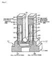
- FIG. 3 is a perspective view schematically showing the quartz resonator in FIG. 1.
- the excitation electrode and the pull out electrode will be explained in reference to these drawings.
- the quartz resonator is provided with one electrode and the other electrode making a pair, one and the other electrodes.
- the one electrode 41 is formed between the whole inside surfaces of two grooves 31 and 32 of the vibrating arm 2a and the space formed between these grooves 31, 32.
- the excitation electrode 4 formed on a so-called bridge which corresponds to the space between the grooves 31 and 32, the excitation electrodes 41, 41 in the respective grooves 31, 32 of the vibrating arm 2a are connected.
- the other electrode 51 is formed on both sides 21 and 21 of the vibrating arm 2a and a portion on the main surfaces 22 and 22 (front and back) upper than the second groove 31 on the front-end side.
- an adjusting weight 50 which is a metal film to adjust the oscillation frequency by changing the weight of the arm.
- the adjusting weight 50 is a portion of the excitation electrode 51, but differs in, for instance, thickness of the film or the material of the electrode from other portion of the electrode. Note that the excitation electrodes 41 and 51 are expressed using a slanting line area and a black dot area to make the drawing easier to see in FIG. 3. Therefore, the slanting lines in FIG. 3 are not for showing a cross section.
- the other excitation electrode 51 is formed on the whole inside surfaces of the two grooves 31 and 32 of the vibrating arm 2b and the space between these grooves 31 and 32.
- the one electrode 41 is formed on both side surfaces 21 and 21 of the vibrating arm 2b and a portion on the main surfaces 22 and 22 (front and back) upper than the second groove 32 on the front-end side.
- an adjusting weight 40 is provided at the front-end of the arm 2a to adjust the oscillation frequency by changing the weight of the arm in a similar fashion.
- the arrangement of the electrodes provided on the vibrating arms 2a and 2b are similar to each other except that the excitation electrodes 41 and 51 are in reverse relation.
- An electrode pattern consisting of a pull out electrode 42 is formed on the surface of the base 1 so that the one excitation electrodes 41 and 41 are electrically connected, and at the same time, an electrode pattern consisting of a pull out electrode 52 is formed on the surface of the base 1 so that the other excitation electrodes 51 and 51 are electrically connected.
- a chromium (Cr) film for improving the adhesion and a gold (Au) film as a metal mask are formed by a vapor deposition method.
- a resist is coated on the gold (Au) film to expose a gold (Au) film at a place corresponding to an outer frame of the quartz resonator which amount to, for instance, several thousand pieces by photolithography.
- the exposed gold (Au) film and chromium (Cr) film are removed to expose the quartz crystal at this portion.
- the exposed quartz crystal is removed by etching with hydrofluoric acid.
- the resist film is fallen off from the quartz crystal surface by hydrofluoric acid, only the gold (Au) film and its backing chromium (Cr) film which are unaffected by hydrofluoric acid still remain.
- the resist film is coated again on both surfaces of the original form 6, and the gold (Au) film at the place corresponding to the grooves 31 and 32 of respective quartz resonators are exposed by photolithography. Then, using a potassium iodide (KI) solution, the exposed gold (Au) film and the chromium (Cr) film are removed to expose the quartz crystal at this place.
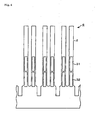
- the grooves 31 and 32 are formed at portions corresponding to the respective vibrating arms 2 of the original form 6 by removing a portion of the exposed quartz crystal by etching with hydrofluoric acid as shown in FIG. 4.
- an n-type amorphous silicon film (referred to as a silicon film hereinafter) in which, for instance, phosphorus (P) is doped as an impurity) is deposited on both surfaces of the original form 6 manufactured in the previous process by, for instance, chemical vapor deposition (CVD).
- CVD chemical vapor deposition
- the exposed silicon film is removed by plasma dry etching using a gas such as sulfur hexafluoride (SF 6 ) or the like so that only the electrode pattern remains. Then, only the front-end portions (places corresponding to the adjusting weights 40 and 50 in FIG. 3) of the respective vibrating arms 2 are exposed by removing the resist. Thereafter, the original form 6 is covered with a metal mask, and the adjusting weights 40 and 50 are formed by forming a gold (Au) film on the exposed portion by, for instance, a vacuum evaporation method. After these steps, the original form 6 on which the electrode pattern, etc. are formed is prepared. After measuring and adjusting the oscillation frequency of the original form 6 are conducted, the respective quartz resonators are separated.
- SF 6 sulfur hexafluoride
- the separated quartz resonators are sent to the following packaging process.
- the silicon film formed on the surface of the original form 6 is not limited to the n-type amorphous silicon, it may be a p-type to which, for instance, boron (B) is doped as an impurity.
- B boron
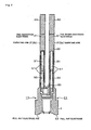
- FIG. 5A is a vertical cross section of the quartz resonator package.
- 7 indicates a package in which the above-described quartz resonator is housed.
- the package 7 includes a case body 7a having an aperture on the upper surface and made of, for instance, ceramic, and a lid body 7b made of, for instance, metal.
- the case body 7a and the lid 7b are seam-welded via, for instance, a sealing compound 7c made of a welding flux, and the inside thereof is in a vacuum state.
- prepared tuning type quartz resonator 70 is fixed to a pedestal portion 71 in the package 7 at portions of the pull out electrodes 42 and 52 of the base 1 with a conductive adhesive 7d, and is disposed horizontally in a state that the vibrating arms 2 are extending in a space inside the package 7.
- the pull out electrodes 42 and 52 are connected to electrodes 74 and 75 disposed so as to face each other in the longitudinal direction of the outside bottom of the case body 7a through conductive paths 72 and 73 (73 is a conductive path on the inner side of the paper depicting FIG.
- the quartz resonator package is installed on a wiring board (not shown) on which circuit parts of an oscillating circuit are installed, and thus a quartz oscillator is completed.
- the quartz resonator package is not limited to that having the SMD structure, it may have a structure in which the quartz resonator is disposed in a metal cylinder sealed at one end thereof with an insulating material, and the respective pull out electrodes are connected to the inner ends of a pair of electrode pins penetrating through the insulating material.
- the quartz resonator relating to the present embodiment will be explained next.
- the electrode patterns of the excitation electrodes 41, 51 or the pull out electrodes 42, 52 formed on the surface of the quartz resonator are made of silicon material.
- the specific gravity of the silicon material is about 2.4 which is about an eighth that of gold (Au) (about 18.9) which is generally used as an electrode.
- the specific gravity of the silicon material is close to that of quartz crystal (about 2.6). Therefore, the quartz resonator using a silicon material as an electrode material becomes small in mass and easier to oscillate compared with gold (Au).
- the value of stiffness of silicon material is closer to quartz crystal compared with gold (Au).
- the electromechanical combination coefficient (a coefficient expressing a capacity to convert electric energy into mechanical (tuning fork oscillation) energy) is large, which makes the CI value expressing difficulty of oscillation low, conversely.
- the silicon material is used as the electrode material, owing to these functions created by using the silicon material, it is expected that the CI value can be reduced to about 35 k ⁇ or lower, whereas the CI value is about 50 k ⁇ to about 100 k ⁇ in the case of the conventional quartz resonator using, for instance, gold (Au). It should be noted that even when the excitation electrodes 41 and 51 are formed with the silicon material, and the pull out electrodes 42 and 52 are formed with other materials, it is still in the cope of the present invention.
- the quartz resonator according to the present invention it is possible to lower the CI value of the quartz resonator by using the silicon material consisting of polysilicon or amorphous silicon. Thereby, it becomes possible to improve the efficiency in converting electric charge into tuning fork oscillation and to lower the consumption energy.
- a tuning fork type quartz resonator having a low CI value and a quartz resonator package provided with the quartz resonator A silicon material lower in specific gravity and stiffness than those of conventionally used gold (Au) is used as an electrode material for an electrode pattern such as excitation electrodes for making the tuning fork type quartz resonator generate tuning fork oscillation.
- the quartz resonator is made easier to oscillate so that the oscillation loss (CI value) can be lowered during conversion of electric energy into tuning fork oscillation.
Landscapes
- Physics & Mathematics (AREA)
- Acoustics & Sound (AREA)
- Chemical & Material Sciences (AREA)
- Crystallography & Structural Chemistry (AREA)
- Engineering & Computer Science (AREA)
- Manufacturing & Machinery (AREA)
- Piezo-Electric Or Mechanical Vibrators, Or Delay Or Filter Circuits (AREA)
Applications Claiming Priority (1)
| Application Number | Priority Date | Filing Date | Title |
|---|---|---|---|
| JP2006100567A JP2007274610A (ja) | 2006-03-31 | 2006-03-31 | 水晶振動子及び水晶振動子パッケージ |
Publications (2)
| Publication Number | Publication Date |
|---|---|
| EP1841064A1 true EP1841064A1 (de) | 2007-10-03 |
| EP1841064B1 EP1841064B1 (de) | 2008-10-15 |
Family
ID=38255282
Family Applications (1)
| Application Number | Title | Priority Date | Filing Date |
|---|---|---|---|
| EP07105353A Active EP1841064B1 (de) | 2006-03-31 | 2007-03-30 | Quarzresonator, Quarzresonatorpaket und Quarzoszillator |
Country Status (8)
| Country | Link |
|---|---|
| US (1) | US20070228897A1 (de) |
| EP (1) | EP1841064B1 (de) |
| JP (1) | JP2007274610A (de) |
| CN (1) | CN101051815B (de) |
| AT (1) | ATE411644T1 (de) |
| DE (1) | DE602007000169D1 (de) |
| DK (1) | DK1841064T3 (de) |
| TW (1) | TW200746629A (de) |
Cited By (1)
| Publication number | Priority date | Publication date | Assignee | Title |
|---|---|---|---|---|
| CN117439571A (zh) * | 2023-11-15 | 2024-01-23 | 成都泰美克晶体技术有限公司 | 一种音叉型石英晶体振荡片及谐振器 |
Families Citing this family (10)
| Publication number | Priority date | Publication date | Assignee | Title |
|---|---|---|---|---|
| JP4539708B2 (ja) * | 2007-11-02 | 2010-09-08 | エプソントヨコム株式会社 | 圧電振動片、圧電振動子および加速度センサ |
| JP2009182555A (ja) * | 2008-01-30 | 2009-08-13 | Seiko Instruments Inc | 圧電振動片、圧電振動子、発振器、電子機器及び電波時計並びに圧電振動片の製造方法 |
| JP2011029715A (ja) | 2009-07-21 | 2011-02-10 | Seiko Instruments Inc | 圧電振動片、圧電振動子、発振器、電子機器及び電波時計並びに圧電振動片の製造方法 |
| US20110215680A1 (en) * | 2010-03-05 | 2011-09-08 | Seiko Epson Corporation | Resonator element, resonator, oscillator, and electronic device |
| KR101129978B1 (ko) * | 2010-07-20 | 2012-03-26 | 주식회사 하이닉스반도체 | 반도체 소자의 제조 방법 |
| JP6390206B2 (ja) * | 2013-09-27 | 2018-09-19 | 株式会社大真空 | 圧電発振器 |
| JP6105648B2 (ja) * | 2015-02-10 | 2017-03-29 | エスアイアイ・クリスタルテクノロジー株式会社 | 圧電振動片、圧電振動子、発振器、電子機器及び電波時計並びに圧電振動片の製造方法 |
| CN111900951A (zh) * | 2020-08-02 | 2020-11-06 | 泰晶科技股份有限公司 | 一种高真空表面贴装的微型音叉石英晶体谐振器 |
| CN111917395A (zh) * | 2020-08-02 | 2020-11-10 | 泰晶科技股份有限公司 | 一种高真空表面贴装的微型音叉石英晶体谐振器及其制作方法 |
| CN119766188A (zh) * | 2024-11-06 | 2025-04-04 | 东南大学 | 一种低阻抗石英音叉谐振器及其制备方法 |
Citations (3)
| Publication number | Priority date | Publication date | Assignee | Title |
|---|---|---|---|---|
| EP0451992A2 (de) * | 1990-04-11 | 1991-10-16 | Wisconsin Alumni Research Foundation | Schwingungserkennung eines Mikrobalkens durch eine Hülle |
| EP1217735A1 (de) * | 2000-12-21 | 2002-06-26 | Eta SA Fabriques d'Ebauches | Zeitbezug mit einem integrierten mikromechanischen Stimmhabelresonator |
| US20040095199A1 (en) * | 2002-11-13 | 2004-05-20 | Kozo Ono | Surface mount crystal unit and surface mount crystal oscillator |
Family Cites Families (17)
| Publication number | Priority date | Publication date | Assignee | Title |
|---|---|---|---|---|
| JPS5166790A (de) * | 1974-12-06 | 1976-06-09 | Matsushita Electric Industrial Co Ltd | |
| JPS5444548Y2 (de) * | 1975-03-05 | 1979-12-21 | ||
| JPS5253685A (en) * | 1975-10-28 | 1977-04-30 | Citizen Watch Co Ltd | Piezoelectric vibrator |
| JPS5799014A (en) * | 1980-12-12 | 1982-06-19 | Seiko Instr & Electronics Ltd | Tuning fork type oscillator |
| JPH06350376A (ja) * | 1993-01-25 | 1994-12-22 | Matsushita Electric Ind Co Ltd | 気密封止された圧電デバイスおよび気密封止パッケージ |
| JPH11177364A (ja) * | 1997-12-16 | 1999-07-02 | Seiko Epson Corp | 圧電素子の製造方法およびレジスト塗布装置 |
| JP3925199B2 (ja) * | 2000-03-03 | 2007-06-06 | 株式会社大真空 | 水晶振動デバイス |
| JP2001336936A (ja) * | 2000-05-29 | 2001-12-07 | Alps Electric Co Ltd | ジャイロスコープおよび入力装置 |
| US7523537B1 (en) * | 2000-07-13 | 2009-04-28 | Custom Sensors & Technologies, Inc. | Method of manufacturing a tuning fork with reduced quadrature errror and symmetrical mass balancing |
| JP2003273649A (ja) * | 2002-01-11 | 2003-09-26 | Piedekku Gijutsu Kenkyusho:Kk | 電子機器 |
| JP4001029B2 (ja) * | 2002-03-25 | 2007-10-31 | セイコーエプソン株式会社 | 音叉型圧電振動片及びその製造方法、圧電デバイス |
| JP2003332872A (ja) * | 2002-05-14 | 2003-11-21 | Seiko Instruments Inc | 圧電振動子およびその製造方法 |
| JP3915640B2 (ja) * | 2002-07-02 | 2007-05-16 | 株式会社大真空 | 水晶z板のエッチング方法及びその方法によって成形された水晶ウェハ |
| JP4281348B2 (ja) * | 2002-12-17 | 2009-06-17 | セイコーエプソン株式会社 | 圧電振動片と圧電振動片を利用した圧電デバイス、ならびに圧電デバイスを利用した携帯電話装置および圧電デバイスを利用した電子機器 |
| JP4292825B2 (ja) * | 2003-02-26 | 2009-07-08 | セイコーエプソン株式会社 | 水晶振動片の製造方法 |
| JP4465710B2 (ja) * | 2004-05-27 | 2010-05-19 | セイコーエプソン株式会社 | 圧電振動片および圧電デバイス |
| JP2006050186A (ja) * | 2004-08-04 | 2006-02-16 | Seiko Epson Corp | 圧電振動片、及びこれを利用した圧電デバイス |
-
2006
- 2006-03-31 JP JP2006100567A patent/JP2007274610A/ja active Pending
-
2007
- 2007-03-13 TW TW096108529A patent/TW200746629A/zh unknown
- 2007-03-28 US US11/729,687 patent/US20070228897A1/en not_active Abandoned
- 2007-03-30 AT AT07105353T patent/ATE411644T1/de active
- 2007-03-30 EP EP07105353A patent/EP1841064B1/de active Active
- 2007-03-30 DE DE602007000169T patent/DE602007000169D1/de active Active
- 2007-03-30 CN CN2007100917326A patent/CN101051815B/zh not_active Expired - Fee Related
- 2007-03-30 DK DK07105353T patent/DK1841064T3/da active
Patent Citations (3)
| Publication number | Priority date | Publication date | Assignee | Title |
|---|---|---|---|---|
| EP0451992A2 (de) * | 1990-04-11 | 1991-10-16 | Wisconsin Alumni Research Foundation | Schwingungserkennung eines Mikrobalkens durch eine Hülle |
| EP1217735A1 (de) * | 2000-12-21 | 2002-06-26 | Eta SA Fabriques d'Ebauches | Zeitbezug mit einem integrierten mikromechanischen Stimmhabelresonator |
| US20040095199A1 (en) * | 2002-11-13 | 2004-05-20 | Kozo Ono | Surface mount crystal unit and surface mount crystal oscillator |
Cited By (1)
| Publication number | Priority date | Publication date | Assignee | Title |
|---|---|---|---|---|
| CN117439571A (zh) * | 2023-11-15 | 2024-01-23 | 成都泰美克晶体技术有限公司 | 一种音叉型石英晶体振荡片及谐振器 |
Also Published As
| Publication number | Publication date |
|---|---|
| US20070228897A1 (en) | 2007-10-04 |
| DE602007000169D1 (de) | 2008-11-27 |
| ATE411644T1 (de) | 2008-10-15 |
| CN101051815A (zh) | 2007-10-10 |
| EP1841064B1 (de) | 2008-10-15 |
| DK1841064T3 (da) | 2009-01-19 |
| JP2007274610A (ja) | 2007-10-18 |
| TW200746629A (en) | 2007-12-16 |
| CN101051815B (zh) | 2012-06-27 |
Similar Documents
| Publication | Publication Date | Title |
|---|---|---|
| EP1841064B1 (de) | Quarzresonator, Quarzresonatorpaket und Quarzoszillator | |
| CN1292535C (zh) | 包括集成微机械音叉谐振器的时基 | |
| CN102487267B (zh) | 压电振动元件及其制造方法、压电振子及压电振荡器 | |
| US7368861B2 (en) | Piezoelectric resonator element and piezoelectric device | |
| JP4415389B2 (ja) | 圧電デバイス | |
| KR100802865B1 (ko) | 압전 진동편 및 압전 장치 | |
| US8174171B2 (en) | Piezoelectric vibrating devices having bisymmetric vibrating arms and supporting arms, and devices comprising same | |
| GB2043995A (en) | Contour vibration mode piezo-electric resonator | |
| JP2010098531A (ja) | 圧電振動片および圧電デバイス | |
| CN1604466A (zh) | 压电器件和使用压电器件的移动电话装置及电子设备 | |
| JP5062413B2 (ja) | 音叉型圧電振動片及び音叉型圧電振動子 | |
| JP2006311090A (ja) | 圧電振動片および圧電デバイス | |
| JP4569450B2 (ja) | Atカット水晶片の集合体、atカット水晶デバイス、及びatカット水晶デバイスの製造方法 | |
| JP2009081520A (ja) | 水晶振動片および水晶デバイス | |
| JP5154977B2 (ja) | 圧電振動片、圧電デバイス及び音叉型圧電振動子の周波数調整方法 | |
| JP2012161104A (ja) | 音叉型圧電振動片および振動デバイス | |
| JP2009152989A (ja) | 圧電振動片及び圧電デバイス | |
| JP3010922B2 (ja) | 温度検出用水晶振動子及びその製造方法 | |
| JP2013207509A (ja) | 圧電振動片およびその製造方法 | |
| JP2008136095A (ja) | 音叉型圧電振動片および圧電デバイス | |
| JP2005192088A (ja) | 圧電振動片および圧電振動デバイス | |
| JP2007097042A (ja) | 水晶振動板 | |
| JP4020031B2 (ja) | 圧電振動片と圧電振動片を利用した圧電デバイス、ならびに圧電デバイスを利用した携帯電話装置および圧電デバイスを利用した電子機器 | |
| JP2014022792A (ja) | 圧電振動子 | |
| JP2004015562A (ja) | 圧電デバイス |
Legal Events
| Date | Code | Title | Description |
|---|---|---|---|
| PUAI | Public reference made under article 153(3) epc to a published international application that has entered the european phase |
Free format text: ORIGINAL CODE: 0009012 |
|
| AK | Designated contracting states |
Kind code of ref document: A1 Designated state(s): AT BE BG CH CY CZ DE DK EE ES FI FR GB GR HU IE IS IT LI LT LU LV MC MT NL PL PT RO SE SI SK TR |
|
| AX | Request for extension of the european patent |
Extension state: AL BA HR MK YU |
|
| GRAP | Despatch of communication of intention to grant a patent |
Free format text: ORIGINAL CODE: EPIDOSNIGR1 |
|
| 17P | Request for examination filed |
Effective date: 20080310 |
|
| AKX | Designation fees paid |
Designated state(s): AT BE BG CH CY CZ DE DK EE ES FI FR GB GR HU IE IS IT LI LT LU LV MC MT NL PL PT RO SE SI SK TR |
|
| GRAS | Grant fee paid |
Free format text: ORIGINAL CODE: EPIDOSNIGR3 |
|
| GRAA | (expected) grant |
Free format text: ORIGINAL CODE: 0009210 |
|
| AK | Designated contracting states |
Kind code of ref document: B1 Designated state(s): AT BE BG CH CY CZ DE DK EE ES FI FR GB GR HU IE IS IT LI LT LU LV MC MT NL PL PT RO SE SI SK TR |
|
| REG | Reference to a national code |
Ref country code: GB Ref legal event code: FG4D Ref country code: CH Ref legal event code: EP |
|
| REG | Reference to a national code |
Ref country code: CH Ref legal event code: NV Representative=s name: E. BLUM & CO. AG PATENT- UND MARKENANWAELTE VSP |
|
| REG | Reference to a national code |
Ref country code: IE Ref legal event code: FG4D |
|
| REF | Corresponds to: |
Ref document number: 602007000169 Country of ref document: DE Date of ref document: 20081127 Kind code of ref document: P |
|
| REG | Reference to a national code |
Ref country code: DK Ref legal event code: T3 |
|
| REG | Reference to a national code |
Ref country code: SE Ref legal event code: TRGR |
|
| NLV1 | Nl: lapsed or annulled due to failure to fulfill the requirements of art. 29p and 29m of the patents act | ||
| PG25 | Lapsed in a contracting state [announced via postgrant information from national office to epo] |
Ref country code: LT Free format text: LAPSE BECAUSE OF FAILURE TO SUBMIT A TRANSLATION OF THE DESCRIPTION OR TO PAY THE FEE WITHIN THE PRESCRIBED TIME-LIMIT Effective date: 20081015 Ref country code: ES Free format text: LAPSE BECAUSE OF FAILURE TO SUBMIT A TRANSLATION OF THE DESCRIPTION OR TO PAY THE FEE WITHIN THE PRESCRIBED TIME-LIMIT Effective date: 20090126 Ref country code: BG Free format text: LAPSE BECAUSE OF FAILURE TO SUBMIT A TRANSLATION OF THE DESCRIPTION OR TO PAY THE FEE WITHIN THE PRESCRIBED TIME-LIMIT Effective date: 20090115 |
|
| PGFP | Annual fee paid to national office [announced via postgrant information from national office to epo] |
Ref country code: AT Payment date: 20090323 Year of fee payment: 3 Ref country code: DK Payment date: 20090321 Year of fee payment: 3 |
|
| PG25 | Lapsed in a contracting state [announced via postgrant information from national office to epo] |
Ref country code: PT Free format text: LAPSE BECAUSE OF FAILURE TO SUBMIT A TRANSLATION OF THE DESCRIPTION OR TO PAY THE FEE WITHIN THE PRESCRIBED TIME-LIMIT Effective date: 20090316 Ref country code: LV Free format text: LAPSE BECAUSE OF FAILURE TO SUBMIT A TRANSLATION OF THE DESCRIPTION OR TO PAY THE FEE WITHIN THE PRESCRIBED TIME-LIMIT Effective date: 20081015 Ref country code: IS Free format text: LAPSE BECAUSE OF FAILURE TO SUBMIT A TRANSLATION OF THE DESCRIPTION OR TO PAY THE FEE WITHIN THE PRESCRIBED TIME-LIMIT Effective date: 20090215 Ref country code: PL Free format text: LAPSE BECAUSE OF FAILURE TO SUBMIT A TRANSLATION OF THE DESCRIPTION OR TO PAY THE FEE WITHIN THE PRESCRIBED TIME-LIMIT Effective date: 20081015 Ref country code: NL Free format text: LAPSE BECAUSE OF FAILURE TO SUBMIT A TRANSLATION OF THE DESCRIPTION OR TO PAY THE FEE WITHIN THE PRESCRIBED TIME-LIMIT Effective date: 20081015 Ref country code: SI Free format text: LAPSE BECAUSE OF FAILURE TO SUBMIT A TRANSLATION OF THE DESCRIPTION OR TO PAY THE FEE WITHIN THE PRESCRIBED TIME-LIMIT Effective date: 20081015 |
|
| PGFP | Annual fee paid to national office [announced via postgrant information from national office to epo] |
Ref country code: FI Payment date: 20090325 Year of fee payment: 3 |
|
| PG25 | Lapsed in a contracting state [announced via postgrant information from national office to epo] |
Ref country code: EE Free format text: LAPSE BECAUSE OF FAILURE TO SUBMIT A TRANSLATION OF THE DESCRIPTION OR TO PAY THE FEE WITHIN THE PRESCRIBED TIME-LIMIT Effective date: 20081015 Ref country code: RO Free format text: LAPSE BECAUSE OF FAILURE TO SUBMIT A TRANSLATION OF THE DESCRIPTION OR TO PAY THE FEE WITHIN THE PRESCRIBED TIME-LIMIT Effective date: 20081015 Ref country code: BE Free format text: LAPSE BECAUSE OF FAILURE TO SUBMIT A TRANSLATION OF THE DESCRIPTION OR TO PAY THE FEE WITHIN THE PRESCRIBED TIME-LIMIT Effective date: 20081015 |
|
| PLBE | No opposition filed within time limit |
Free format text: ORIGINAL CODE: 0009261 |
|
| STAA | Information on the status of an ep patent application or granted ep patent |
Free format text: STATUS: NO OPPOSITION FILED WITHIN TIME LIMIT |
|
| PG25 | Lapsed in a contracting state [announced via postgrant information from national office to epo] |
Ref country code: CZ Free format text: LAPSE BECAUSE OF FAILURE TO SUBMIT A TRANSLATION OF THE DESCRIPTION OR TO PAY THE FEE WITHIN THE PRESCRIBED TIME-LIMIT Effective date: 20081015 |
|
| PGFP | Annual fee paid to national office [announced via postgrant information from national office to epo] |
Ref country code: SE Payment date: 20090325 Year of fee payment: 3 |
|
| 26N | No opposition filed |
Effective date: 20090716 |
|
| PG25 | Lapsed in a contracting state [announced via postgrant information from national office to epo] |
Ref country code: SK Free format text: LAPSE BECAUSE OF FAILURE TO SUBMIT A TRANSLATION OF THE DESCRIPTION OR TO PAY THE FEE WITHIN THE PRESCRIBED TIME-LIMIT Effective date: 20081015 |
|
| PG25 | Lapsed in a contracting state [announced via postgrant information from national office to epo] |
Ref country code: MC Free format text: LAPSE BECAUSE OF NON-PAYMENT OF DUE FEES Effective date: 20090331 |
|
| REG | Reference to a national code |
Ref country code: IE Ref legal event code: MM4A |
|
| PG25 | Lapsed in a contracting state [announced via postgrant information from national office to epo] |
Ref country code: IE Free format text: LAPSE BECAUSE OF NON-PAYMENT OF DUE FEES Effective date: 20090330 |
|
| PG25 | Lapsed in a contracting state [announced via postgrant information from national office to epo] |
Ref country code: GR Free format text: LAPSE BECAUSE OF FAILURE TO SUBMIT A TRANSLATION OF THE DESCRIPTION OR TO PAY THE FEE WITHIN THE PRESCRIBED TIME-LIMIT Effective date: 20090116 |
|
| EUG | Se: european patent has lapsed | ||
| REG | Reference to a national code |
Ref country code: DK Ref legal event code: EBP |
|
| PG25 | Lapsed in a contracting state [announced via postgrant information from national office to epo] |
Ref country code: FI Free format text: LAPSE BECAUSE OF NON-PAYMENT OF DUE FEES Effective date: 20100330 |
|
| PG25 | Lapsed in a contracting state [announced via postgrant information from national office to epo] |
Ref country code: DK Free format text: LAPSE BECAUSE OF NON-PAYMENT OF DUE FEES Effective date: 20100331 Ref country code: LU Free format text: LAPSE BECAUSE OF NON-PAYMENT OF DUE FEES Effective date: 20090330 |
|
| PG25 | Lapsed in a contracting state [announced via postgrant information from national office to epo] |
Ref country code: HU Free format text: LAPSE BECAUSE OF FAILURE TO SUBMIT A TRANSLATION OF THE DESCRIPTION OR TO PAY THE FEE WITHIN THE PRESCRIBED TIME-LIMIT Effective date: 20090416 |
|
| PG25 | Lapsed in a contracting state [announced via postgrant information from national office to epo] |
Ref country code: TR Free format text: LAPSE BECAUSE OF FAILURE TO SUBMIT A TRANSLATION OF THE DESCRIPTION OR TO PAY THE FEE WITHIN THE PRESCRIBED TIME-LIMIT Effective date: 20081015 |
|
| PG25 | Lapsed in a contracting state [announced via postgrant information from national office to epo] |
Ref country code: CY Free format text: LAPSE BECAUSE OF FAILURE TO SUBMIT A TRANSLATION OF THE DESCRIPTION OR TO PAY THE FEE WITHIN THE PRESCRIBED TIME-LIMIT Effective date: 20081015 |
|
| REG | Reference to a national code |
Ref country code: CH Ref legal event code: PL |
|
| PGFP | Annual fee paid to national office [announced via postgrant information from national office to epo] |
Ref country code: IT Payment date: 20100331 Year of fee payment: 4 |
|
| PG25 | Lapsed in a contracting state [announced via postgrant information from national office to epo] |
Ref country code: CH Free format text: LAPSE BECAUSE OF NON-PAYMENT OF DUE FEES Effective date: 20110331 Ref country code: LI Free format text: LAPSE BECAUSE OF NON-PAYMENT OF DUE FEES Effective date: 20110331 |
|
| PG25 | Lapsed in a contracting state [announced via postgrant information from national office to epo] |
Ref country code: SE Free format text: LAPSE BECAUSE OF NON-PAYMENT OF DUE FEES Effective date: 20100331 |
|
| REG | Reference to a national code |
Ref country code: AT Ref legal event code: MM01 Ref document number: 411644 Country of ref document: AT Kind code of ref document: T Effective date: 20120330 |
|
| PG25 | Lapsed in a contracting state [announced via postgrant information from national office to epo] |
Ref country code: AT Free format text: LAPSE BECAUSE OF NON-PAYMENT OF DUE FEES Effective date: 20120330 |
|
| PGFP | Annual fee paid to national office [announced via postgrant information from national office to epo] |
Ref country code: FR Payment date: 20140311 Year of fee payment: 8 |
|
| PGFP | Annual fee paid to national office [announced via postgrant information from national office to epo] |
Ref country code: GB Payment date: 20140326 Year of fee payment: 8 |
|
| PGFP | Annual fee paid to national office [announced via postgrant information from national office to epo] |
Ref country code: DE Payment date: 20140417 Year of fee payment: 8 |
|
| REG | Reference to a national code |
Ref country code: DE Ref legal event code: R119 Ref document number: 602007000169 Country of ref document: DE |
|
| GBPC | Gb: european patent ceased through non-payment of renewal fee |
Effective date: 20150330 |
|
| REG | Reference to a national code |
Ref country code: FR Ref legal event code: ST Effective date: 20151130 |
|
| PG25 | Lapsed in a contracting state [announced via postgrant information from national office to epo] |
Ref country code: GB Free format text: LAPSE BECAUSE OF NON-PAYMENT OF DUE FEES Effective date: 20150330 Ref country code: DE Free format text: LAPSE BECAUSE OF NON-PAYMENT OF DUE FEES Effective date: 20151001 |
|
| PG25 | Lapsed in a contracting state [announced via postgrant information from national office to epo] |
Ref country code: FR Free format text: LAPSE BECAUSE OF NON-PAYMENT OF DUE FEES Effective date: 20150331 |