EP1841084B1 - Appareil de communication radio et procédé de communication radio - Google Patents
Appareil de communication radio et procédé de communication radio Download PDFInfo
- Publication number
- EP1841084B1 EP1841084B1 EP07006605A EP07006605A EP1841084B1 EP 1841084 B1 EP1841084 B1 EP 1841084B1 EP 07006605 A EP07006605 A EP 07006605A EP 07006605 A EP07006605 A EP 07006605A EP 1841084 B1 EP1841084 B1 EP 1841084B1
- Authority
- EP
- European Patent Office
- Prior art keywords
- signal
- power
- transmission
- received
- output
- Prior art date
- Legal status (The legal status is an assumption and is not a legal conclusion. Google has not performed a legal analysis and makes no representation as to the accuracy of the status listed.)
- Ceased
Links
Images






Classifications
-
- H—ELECTRICITY
- H04—ELECTRIC COMMUNICATION TECHNIQUE
- H04B—TRANSMISSION
- H04B1/00—Details of transmission systems, not covered by a single one of groups H04B3/00 - H04B13/00; Details of transmission systems not characterised by the medium used for transmission
- H04B1/38—Transceivers, i.e. devices in which transmitter and receiver form a structural unit and in which at least one part is used for functions of transmitting and receiving
- H04B1/40—Circuits
- H04B1/50—Circuits using different frequencies for the two directions of communication
- H04B1/52—Hybrid arrangements, i.e. arrangements for transition from single-path two-direction transmission to single-direction transmission on each of two paths or vice versa
- H04B1/525—Hybrid arrangements, i.e. arrangements for transition from single-path two-direction transmission to single-direction transmission on each of two paths or vice versa with means for reducing leakage of transmitter signal into the receiver
Definitions
- the present invention relates to a radio communication apparatus and a radio communication method in which transmission and reception are simultaneously performed using the same carrier frequency.
- interference occurs due to imperfections in a circulator which results in signals from a transmission RF signal processor leaking into a received RF signal processor. Further interference is caused by the effects of reflection and diffraction and so on of the propagation path that result in the transmitted signal transmitted from an antenna being received by the same antenna. These interferences are referred to as "coupling loop interference". Employment of a signal consisting of the coupling loop interference signal described above overlaid on a desired signal transmitted from one radio communication apparatus to another radio communication apparatus requires that the desired signal be detected by the receiving radio communication apparatus, however if the coupling loop interference signal power is large the desired signal cannot be accurately detected. Notably, the effect of coupling loop interference attributable to imperfections of the circulator is comparatively much worse than the effect of coupling loop interference caused by a signal being received again once it has been transmitted from the antenna.
- US Laid-open Gazette Patent Application No.2004/0142700 discloses a method of interference removal in a baseband digital domain employing a radio communication apparatus with a coupling loop interference signal removal function.
- a radio communication apparatus with a coupling loop interference signal removal function described as a booster.
- the cited references “ Suzuki, Ebine, "Configuration and characteristics of an open space booster device for radio paging systems", 1996 IEIEC Annual Conference, B-428, pp.428, Mar. 1996 “ (hereinafter referred to as “cited reference 1") and “ H. Suzuki, K. Itoh, Y. Ebine, M. Sato, "A booster configuration with adaptive reduction of transmitter-receiver antenna coupling for pager systems", Proc. of 50th IEEE Vehicular Technology Conference, VTC 1999-Fall, vol. 3, pp. 1516-1520, Sept.
- cited reference 2 1999 “ (hereinafter referred to as “cited reference 2”) describe boosters for radio paging systems notable in that interference removal in an RF band which constitutes the analog domain and interference removal in the baseband band which constitutes the digital domain are simultaneously performed.
- the cited reference “ Imamura, Hamasumi, Shibuya, Sasaki, "A fundamental study of loop coupling cancellers for broadcast-wave relay in digital terrestrial broadcasting SFN", The Journal of the Institute of Image Information and Television Engineers, vol. 54, No. 11, pp. 1568-1575, 2000 “ (hereinafter referred to as “cited reference 3”) describes a booster for digital terrestrial broadcasting that performs interference removal at the IF band or baseband band.
- cited reference Maeyama, Inoue, Kamimura, Yamato, "Development of a CDMA repeater comprising an interference wave reducing function", 2002 IEIEC Annual Conference, B-5-62, pp. 512, March 2002 " (hereinafter referred to as "cited reference 4"), describes a CDMA signal booster that performs interference cancellation only at the RF band.
- the signal saturation effect at the received RF signal processors can be reduced by removing the interference in the analog domain prior to the signal being received by the received RF signal processors, in this case as well, because of the limit value of the magnitude of the input power for correct operation of the interference remover in the analog domain, signal saturation occurs when a signal in which the limit value is exceeded is input into the interference remover of the analog domain.
- the interference removal characteristics produced by the interference removal performed at the analog domain which constitutes the RF band and the digital domain which constitutes the baseband band are insufficient and, accordingly, a marked deterioration in the detected characteristics of the desired signal occurs.
- US 2004/142700 A1 discloses subtracting a transmitted signal from a received signal in a base station that sends and receives at the same frequency at the same time.
- US 2005/207509 A1 discloses an apparatus comprising a transmitter, a receiver, an antenna and a signal cancellation circuit, wherein the signal cancellation circuit is configured to phase shift a first portion of a transmitter signal to produce a phase-shifted signal, to combine the phase-shifted signal with a second portion of the transmitter signal to produce a combined signal, wherein the second portion of the transmitter signal is associated with a reflection of a third portion of the transmitter signal from the antenna.
- WO 96/15596 discloses a full-duplex radio transceiver, in which the transmission signal is sampled, and the gain and phase of the sampled signal are controllably adjusted, before subtracting the adjusted signal from the received signals.
- the radio communication apparatus pertaining to the present invention for resolving the problems described above constitutes a radio communication apparatus for performing transmission and reception based on radio communication including: a power suppressor for coupling loop interference signal for attenuating signal power of a received signal in order to suppress coupling loop interference signal power of the received signal; a transceiver having a coupling loop interference signal removal function for analog domain and a coupling loop interference signal removal function for digital domain, for removing a coupling loop interference signal contained in a signal output from the power suppressor for coupling loop interference signal; a baseband signal processor having a transmission baseband signal processor and a received baseband signal processor; a fluctuation determiner for received signal power for determining received signal power fluctuation speed employing an output signal on which interference removal for analog domain has been performed by the transceiver; a power determiner for residual interference signal for determining a ratio of residual interference signal power in the output signal power on which interference removal for digital domain has been performed by the transceiver; and a transmission propriety/improprie
- the signal saturation effect can be reduced by the transceiver.
- an adaptive interference canceller in the analog domain, for example is employed by the transceiver, this adaptive interference canceller can reduce the signal saturation effect.
- the transceiver of the radio communication apparatus pertaining to the present invention includes a baseband signal processor having a transmission baseband signal processor and a received baseband signal processor, and the baseband signal processor is desirably configured so that output from the received baseband signal processor is input into the transmission baseband signal processor. That is to say, the transmission baseband signal processor generates a transmit signal using data input from the received baseband signal processor.
- the radio communication apparatus pertaining to the present invention can be employed as a booster in a TDD system, and the signal saturation effect caused by the coupling loop interference signal can be reduced.
- the transceiver of the radio communication apparatus pertaining to the present invention further includes a transmission RF signal processor and a received RF signal processor
- the radio communication apparatus further includes a controller for power suppression for controlling at least one of the magnitude of the signal power attenuated by the power suppressor for coupling loop interference signal, the magnitude of the output power of the transmission RF signal processor, the magnitude of the output power of the received RF signal processor, and the magnitude of the output of the baseband signal processor
- the controller for power suppression is desirably configured to perform the control in response to at least one of the magnitude of the output power of the transmission RF signal processor, the magnitude of the output power of the received RF signal processor, and the magnitude of the output of the baseband signal processor.
- the signal saturation effect can be further reduced because the magnitudes of output are controllable in response to permissible outputs which differ for each of the transmission RF signal processor, the received RF signal processor and the baseband signal processor.
- the radio communication apparatus pertaining to the present invention further includes a fluctuation determiner for received signal power for determining received signal power fluctuation speed employing an output signal on which analog domain interference removal has been performed by the transceiver, a power determiner for residual interference signal for determining the ratio of residual interference signal power in the output signal power on which digital domain interference removal has been performed by the transceiver, and a transmission propriety/impropriety decider for determining the propriety of transmission from the transmission baseband signal processor in accordance with at least one of whether or not the received signal power fluctuation speed determined by the fluctuation determiner for received signal power is equal to or greater than a predetermined standard value and whether or not the ratio of residual interference signal power determined by the power determiner for residual interference signal is equal to or greater than a predetermined standard value, and wherein the transmission baseband signal processor is desirably configured to perform a signal transmission execution/stoppage control in response to the transmission propriety result decided by the transmission propriety/impropriety decider.
- signal transmission propriety can be determined in response to at least one of the fluctuation speed of the received signal power or the ratio of the residual interference signal power. For this reason, when the signal saturation effect is too large and sufficient interference removal characteristics cannot be produced, transmission is determined as being improper and signal transmission can be stopped. Deterioration of the signal detected characteristics of the desired signal can be prevented in this way.
- the radio communication method pertaining to the present invention for resolving the problems described above constitutes a radio communication method of a radio communication apparatus for performing transmission and reception based on radio communication including: a power suppression step of attenuating signal power of a received signal to suppress the coupling loop interference signal power of the received signal; a removing step of performing a coupling loop interference signal removal processing for analog domain and coupling loop interference signal removal processing for digital domain, to remove a coupling loop interference signal contained in an output signal by the power suppression step; a fluctuation determining step of determining received signal power fluctuation speed employing an output signal on which interference removal for analog domain has been performed in the removing step; a power determining step of determining a ratio of residual interference signal power in the output signal power on which interference removal for digital domain has been performed in the removing step; and a transmission propriety/impropriety deciding step of determining the propriety of transmission from a transmission baseband signal processor in accordance with at least one of whether or not the received signal power fluctuation speed determined by
- the radio communication method pertaining to the present invention further includes: a control step of performing control on at least one of the magnitude of the signal power attenuated in the power suppression step, the magnitude of the output power by transmission RF signal processing in the removing step, the magnitude of the output power by received RF signal processing in the removing step, and the magnitude of the output by baseband signal processing in the removing step, and wherein the control is performed in response to at least one of the magnitude of the output power by the transmission RF signal processing, the magnitude of the output power by the received RF signal processing, and the magnitude of the output by the baseband signal processing.
- the signal saturation effect can be further reduced because the magnitudes of output are controllable in response to permissible outputs which differ for each of the transmission RF signal processor, the received RF signal processor and the baseband signal processor.
- the signal saturation effect in radio communication in which transmission and reception are simultaneously performed using the same carrier frequency can be reduced.
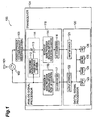
- FIG. 1 is a hardware block diagram of a radio communication apparatus pertaining to a first arrangement.
- FIG. 2 is a function block diagram of a digital signal processor pertaining to the first arrangement.
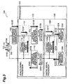
- FIG. 3 is a block diagram illustrating an operation protocol of the radio communication apparatus pertaining to the first arrangement.
- FIG. 4 is a diagram showing a first modification of the hardware block diagram of the radio communication apparatus pertaining to a first arrangement.
- FIG. 5 is a diagram showing a second modification of the hardware block diagram of the radio communication apparatus pertaining to a first arrangement.
- FIG. 6 is a diagram showing a first modification of the operation protocol of the radio communication apparatus pertaining to the first arrangement.
- FIG. 7 is a diagram showing a second modification of the operation protocol of the radio communication apparatus pertaining to the first arrangement.
- FIG. 8 is a function block diagram of a digital signal processor pertaining to a second arrangement.
- FIG. 9 is a diagram showing an operation protocol of a radio communication apparatus pertaining to the second arrangement.
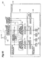
- FIG. 10 is a hardware block diagram of a radio communication apparatus pertaining to a third arrangement.
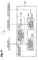
- FIG. 11 is a function block diagram of a digital signal processor pertaining to the third arrangement.
- FIG. 12 is a diagram showing an operation protocol of the radio communication apparatus pertaining to the third arrangement.
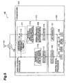
- FIG. 13 is a hardware block diagram of a radio communication apparatus pertaining to a fourth arrangement.
- FIG. 14 is a function block diagram of a digital signal processor pertaining to the fourth arrangement.
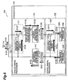
- FIG. 15 is a diagram showing an operation protocol of the radio communication apparatus pertaining to the fourth arrangement.
- radio communication apparatus pertaining to an arrangement of the present disclosure will be hereinafter described with reference to the drawings. Where possible; identical symbols have been assigned to identical sections and a replication of the description thereof has been omitted.
- FIG. 1 is a hardware configuration diagram of this radio communication apparatus.
- the radio communication apparatus 100 is physically configured to include an antenna 101, a circulator 102, a power suppressor for coupling loop interference signal 103, and a transceiver 104 with a coupling loop interference removal function.
- the transceiver 104 is configured to include an analog signal processor 110 and a digital signal processor 120.
- the analog signal processor 110 is configured to include an analog domain interference canceller 111, a received RF signal processor 114, a transmission RF signal processor 115, an A/D converter 116 and a D/A converter 117.
- the analog domain interference canceller 111 is configured to include an analog signal generator for interference removal 112 and analog domain interference signal remover 113.
- the digital signal processor 120 is configured to include an input interface 121, an output interface 122, a CPU 123, a RAM 124 and ROM 125 serving as a primary memory, and a secondary memory 126 such as a hard disk or the like.
- the power suppressor for coupling loop interference signal 103 of this configuration attenuates the signal power of a signal received by the antenna 101 in order to suppress the coupling loop interference signal power contained in the received signal.
- the transceiver 104 with the coupling loop interference removal function removes the coupling loop interference signal contained in the received signal from which the signal power has been attenuated by way of the interference canceller 111.
- the signal saturation effect can be subsequently reduced by the interference canceller 111.
- the removal characteristics of the analog domain coupling loop interference signal can be improved.
- FIG. 2 is a function block diagram of the digital signal processor 120 of this arrangement.
- the digital signal processor 120 is configured to include a digital domain interference canceller 1201 and baseband signal processor 1204.
- the interference canceller 1201 is configured to include an digital signal generator for interference removal 1202 and an interference signal remover for digital domain 1203.
- the baseband signal processor 1204 is configured to include a received baseband signal processor 1205 and a transmission baseband signal processor 1206.
- the interference canceller 1201 removes the coupling loop interference signal component residually contained in the signal converted into a digital signal by the A/D converter 116.
- the removal described above is performed by the interference canceller 1201 at this time by deduction of the signal generated by the digital signal generator for interference removal 1202 employing the output signal of the transmission baseband signal processor 1206, from the output signal of the A/D converter 116. While the removal characteristics for coupling loop interference signal differ markedly in the digital domain due to the signal saturation effect in the analog signal processor 110, the removal characteristics of the digital domain coupling loop interference signal can be improved by attenuation of the signal power by the power suppressor for coupling loop interference signal 103.
- FIG. 3 is a block diagram illustrating an operation protocol of the radio communication apparatus pertaining to this arrangement.
- the transmission baseband signal processor 1206 generates a signal for transmission.
- the output of the transmission baseband signal processor 1206 is input into the digital signal generator for interference removal 1202 and, in addition, is input into the D/A converter 117.
- the signal input into the D/A converter 117 is converted into an analog signal and input into the transmission RF signal processor 115.
- the signal is converted in the transmission RF signal processor 115 to an RF band analog signal by signal amplification performed by an amplifier, bandwidth limitation performed by a filter, and frequency conversion performed by an up converter, the converted signal being input into the analog signal generator for interference removal 112 and input into the circulator 102.
- step S103 the signal input into the circulator 102 is received by way of the antenna 101.
- part of the signal input into the circulator 102 is supplied to the power suppressor for coupling loop interference signal 103 where it forms a coupling loop interference signal.
- the desired signal transmitted from a radio to the receiving radio 100 and the coupling loop interference signal of the signal transmitted in step S103 are received by the antenna 101 and, in step S104, are supplied to the coupling loop interference signal reducer 103.
- the power suppressor for coupling loop interference signal 103 attenuates the signal power in step S105 to suppress the signal saturation effect in the analog signal processor 110 and then inputs the signal into the analog domain interference signal remover 113.
- step S107 the analog domain interference signal remover 113 performs interference removal employing a signal generated by the analog signal generator for interference removal 112 in step S106.
- the analog signal generator for interference removal 112 generates an interference removal analog signal employing the output signal of the transmission RF signal processor 115 generated in step S102.
- the signal on which interference removal has been performed in the analog domain is input into the received RF signal processor 114 whereupon, in step S108, signal amplification by means of an amplifier, bandwidth limitation by means of a filter, and frequency conversion by means of a down converter and so on are performed on the signal in received RF signal processor 114.
- step S108 The signal obtained by the processing of step S108 is input into the A/D converter 116 and, in step S109, is converted into a digital signal by the A/D converter 116, the converted signal being then input into the interference signal remover for digital domain 1203.
- the interference signal remover for digital domain 1203 performs interference removal employing the signal generated by the digital signal generator for interference removal 1202 generated in step S 110.
- the digital signal generator for interference removal 1202 generates a digital domain interference removal signal employing the signal generated by the transmission baseband signal processor 1206 in step S 100.
- step S112 the signal on which interference removal has been performed by the interference signal remover for digital domain 1203 is input into the received baseband signal processor 1205 where desired signal detection is performed.
- step S105 By attenuation of the signal power in order to reduce the coupling loop interference signal power in step S105 as described above, the signal saturation effect in the removal of the coupling loop interference signal of the analog domain in step S107 and in the removal of the coupling loop interference signal in the digital domain of step S111 is reduced.
- step S105 the signal transmission of the desired signal may be enlarged.
- the signal saturation effect attributable to the coupling loop interference signal to which the analog domain interference canceller 111 and received RF signal processor 114 are subjected can be reduced by attenuation of the signal power by the power suppressor for coupling loop interference signal 103.
- a modification of the configuration of the radio communication apparatus described above will be hereinafter described. While the example configuration of the radio communication apparatus described above describes a configuration in which, as shown in FIG. 1 , the power suppressor for coupling loop interference signal 103 is provided between the circulator 102 and the interference canceller 111, as shown in FIG. 4 , a configuration in which the power suppressor for coupling loop interference signal 103 is provided between the interference canceller 111 and the received RF signal processor 114 may be adopted.
- the signal saturation effect to which the received RF signal processor 114 and A/D converter 116 are subsequently subjected can be reduced by attenuation of the power of the signal from which the coupling loop interference signal has been removed by the interference canceller 111 by the power suppressor for coupling loop interference signal 103.
- the power suppressor for coupling loop interference signal 103 is provided between the received RF signal processor 114 and the A/D converter 116 .
- the signal saturation effect to which the A/D converter 116 is subjected can be similarly reduced by attenuation of the signal power by the power suppressor for coupling loop interference signal 103.
- the power suppressor for coupling loop interference signal 103 may be provided in an arbitrary position in the received RF signal processor 114.
- the signal saturation effect can be reduced by provision of the power suppressor for coupling loop interference signal 103 in the configuration of the radio communication apparatus 100 in any position between the circulator 102 and A/D converter 116.
- the radio communication method transmission described above describes a method in which the signal power of the signal supplied to the coupling loop signal power suppressor 103 in step S104 is attenuated in step S105
- the signal power of the signal in which the analog domain interference removal has been performed in step S107 may be attenuated in step S105.
- the signal saturation effect can be reduced in step S 108 and beyond.
- the signal power of the signal on which the received RF signal processing has been performed in step S108 may be attenuated in step S105.
- the signal saturation effect with respect to A/D conversion (step S 109) can be reduced.
- the attenuation processing of the signal power of step S105 may be performed at any stage of the received RF signal processing of step S108.
- the signal saturation effect can be reduced by this radio communication method by executing the signal power attenuation processing of step S105 anywhere between step S104 and step S109.
- FIG. 8 shows a function block diagram of the digital signal processor 120 of this arrangement.
- the baseband signal processor 1204 employs the output signal of the received baseband signal processor 1205 as the input signal of the transmission baseband signal processor 1206.
- FIG. 9 is a diagram showing an operation protocol of a radio communication apparatus pertaining to the second arrangement.
- the baseband signal processor 1204 employs the output signal of the received baseband signal processor 1205 as the input signal of the transmission baseband signal processor 1206.
- the radio communication apparatus 200 can be employed as a booster in a TDD system and, by attenuation of the signal by the power suppressor for coupling loop interference signal 103, the problems inherent to the employment of the radio communication apparatus 200 as a booster in a TDD system, that is to say, the signal saturation effect attributable to the coupling loop interference signal, can be reduced.
- FIG. 10 is a hardware block diagram of a radio communication apparatus pertaining to a third arrangement.
- the radio communication apparatus 300 of this arrangement further includes a controller for power suppression 301 in the configuration of the radio communication apparatus 100 of the first arrangement shown in FIG. 1 .
- the controller for power suppression 301 of this configuration performs the control of at least one of the signal attenuated amount by the power suppressor for coupling loop interference signal 103, the magnitude of the output signal of the received RF signal processor 114, the magnitude of the output signal of the transmission RF signal processor 115, and the magnitude of the output of the digital signal processor 120, in response to at least one of a current output of the received RF signal processor 114, a current output of the transmission RF signal processor 115, and a current output of the digital signal processor 120.
- FIG. 11 is a function block diagram of a digital signal processor 120 pertaining to this arrangement. While the configuration of the digital signal processor 120 is identical to that of the first arrangement, this arrangement is different from the first arrangement in the point that (1) the output of the baseband signal processor 1204 is input into the controller for power suppression 301, (2) the magnitude of the output on which the baseband signal processor 1204 has applied is decided by the controller for power suppression 301, and (3) the magnitude of the output of the transmission baseband signal processor 1206 is controlled by the baseband signal processor 1204 in accordance with this result.
- FIG. 12 is a diagram showing an operation protocol of the radio communication apparatus 300 pertaining to this arrangement.
- the method of radio communication transmission and reception pertaining to this arrangement is notable in that it includes, in addition to the protocol of the first arrangement shown in FIG. 3 , the step S300 to S302, S310 to S312, S320 and S321.
- step S300 simultaneous with input of the magnitude of a current output signal of the transmission RF signal processor 115 into the controller for power suppression 301, in step S301, the magnitude of the current output signal of the received RF signal processor 114 is input into the controller for power suppression 301 and, in step S302, the magnitude of the output of the transmission baseband signal processor 1206 is input into the controller for power suppression 301 in the baseband signal processor 1204.
- step S320 in order to reduce the signal saturation effect, the controller for power suppression 301 determines the signal attenuation amount of the power suppressor for coupling loop interference signal 103, the magnitude of the output signal of the transmission RF signal processor 115, the magnitude of the output signal of the received RF signal processor 114, and the output magnitude of the baseband signal processor 1204.
- the controller for power suppression 301 notifies the power suppressor for coupling loop interference signal 103 (step S321) of the determined signal attenuation amount and, in addition, notifies each of the transmission RF signal processor 115, the received RF signal processor 114 and the baseband signal processor 1204 of the determined output magnitude (steps S310, S311 and S312).
- the power suppressor for coupling loop interference signal 103 employs these values to attenuate the signal and, in addition, each of the transmission RF signal processor 115, received RF signal processor 114 and baseband signal processor 1204 outputs a signal of the notified output magnitude.
- FIG. 13 is a hardware block diagram of a radio communication apparatus pertaining to this arrangement.
- the radio communication apparatus 400 of this arrangement further includes a fluctuation determiner for received signal power 401 in addition to the configuration of the radio communication apparatus 100 of the first arrangement shown in FIG. 1 .
- the fluctuation determiner for received signal power 401 of this configuration has a function for determining speed fluctuation of the received signal power. Satisfactory interference removal characteristics cannot be produced when the received signal power fluctuation is fast and, accordingly, the object of this function is to stop signal transmission from the radio apparatus 400.
- the output of the fluctuation determiner for received signal power 401 is input into the digital signal processor 120, and the digital signal processor 120 determines signal transmission propriety.
- FIG. 14 is a function block diagram of a digital signal processor pertaining to the fourth arrangement.
- the configuration of the digital signal processor 120 is further configured to include a power determiner for residual interference signal 410 and a transmission propriety/impropriety decider 411, in addition to the function block of the first arrangement shown in FIG. 2 .
- the power determiner for residual interference signal 410 determines the power ratio (i.e. ratio of power) of the residual interference signal in the output signal after the interference removal for the digital domain.
- the power ratio of the residual interference signal in the output signal determined by the power determiner for residual interference signal 410 is input into the transmission propriety/impropriety decider 411.
- the transmission propriety/impropriety decider 411 determines whether or not signal transmission is to be performed by the transmission baseband signal processor 1206 in accordance with (1) whether or not the received signal power fluctuation speed determined by the fluctuation determiner for received signal power 401 is equal to or greater than a predetermined standard value and (2) whether or not the power ratio of the output of the residual interference signal determined by the power determiner for residual interference signal 410 is equal to or greater than a predetermined standard value. And the determination of which is input into the baseband signal processor 1204.
- FIG. 15 is a diagram showing an operation protocol of the radio communication apparatus pertaining to this arrangement.
- the protocol pertaining to this arrangement further includes steps S400 to S402 in addition to the protocol of FIG. 3 shown for the first arrangement.
- step S400 the fluctuation speed of the received signal power is determined employing the signal on which the analog domain interference removal of S 107 has been performed.
- the signal prior to analog domain interference removal may be employed or a signal at any stage of the processing in the received RF signal processor 114 may be employed in determining the fluctuation speed of the received signal power of step S400.
- step S401 the power determiner for residual interference signal 410 determines the power of the residual interference signal from the output signal on which digital domain interference removal has been performed, and determines the output ratio of the residual interference signal in the output signal on which the digital domain interference removal has been performed.
- step S402 the transmission propriety/impropriety decider 411 judges whether or not the received signal power fluctuation speed determined in step S400 is equal to or greater than a predetermined standard value and in addition, judges whether or not the output ratio of the residual interference determined in S401 is equal to or greater than a predetermined standard value.
- the transmission propriety/impropriety decider 411 determines that the received signal power fluctuation speed is equal to or greater than a predetermined standard value or the transmission propriety/impropriety decider 411 determines that the output ratio of the residual interference signal is equal to or greater than a than a predetermined standard value, transmission from the transmission baseband signal processor 1206 is determined as improper, and if the received signal power fluctuation speed is determined as being less than the predetermined standard value and the output ratio of the residual interference signal is less than the predetermined standard value, transmission from the transmission baseband signal processor 1206 is determined as being possible.
- the transmission propriety/impropriety decider 411 outputs the determined result to the baseband signal processor 1204.
- a control can be performed when the received signal power fluctuation speed is a predetermined standard value or higher and the power ratio of the residual interference signal is a predetermined standard value or higher to stop transmission from the radio communication apparatus 400.
- the signal saturation effect can be reduced and the desired signal detected characteristics of the received baseband signal processor 1205 can be improved.
Landscapes
- Engineering & Computer Science (AREA)
- Computer Networks & Wireless Communication (AREA)
- Signal Processing (AREA)
- Noise Elimination (AREA)
- Mobile Radio Communication Systems (AREA)
- Transceivers (AREA)
Claims (5)
- Dispositif de radiocommunication (100, 200, 300, 400) servant à effectuer une émission et une réception basées sur une communication radio, comprenant :un élément antiparasite pour un signal d'interférence de boucle de couplage (103) servant à atténuer la puissance de signal d'un signal reçu afin de supprimer la puissance de signal d'interférence de boucle de couplage du signal reçu ;un émetteur-récepteur (104) ayant une fonction de retrait de signal d'interférence de boucle de couplage pour le domaine analogique et une fonction de retrait de signal d'interférence de boucle de couplage pour le domaine numérique, servant à retirer un signal d'interférence de boucle de couplage contenu dans un signal délivré par l'élément de suppression de puissance pour un signal d'interférence de boucle de couplage (103) ;un processeur de signal de bande de base (120) comportant un processeur de signal de bande de base d'émission (1206) et un processeur de signal de bande de base reçu (1205) ;un élément de détermination de fluctuation pour une puissance de signal reçu (401) pour déterminer une vitesse de fluctuation de puissance de signal reçu en utilisant un signal de sortie auquel un retrait d'interférence pour le domaine analogique a été appliqué par l'émetteur-récepteur (104) ;un élément de détermination de puissance pour un signal d'interférence résiduelle (410) pour déterminer un rapport de puissance de signal d'interférence résiduelle dans la puissance du signal de sortie auquel un retrait d'interférence pour le domaine numérique a été appliqué par l'émetteur-récepteur (104) ; etun élément de décision d'opportunité/inopportunité d'émission (411) pour déterminer la propriété d'émission à partir du processeur de signal de bande de base d'émission (1206) au moins selon que la vitesse de fluctuation de puissance de signal reçu déterminée par l'élément de détermination de fluctuation pour une puissance de signal reçu (401) est ou non égale ou supérieure à une valeur standard prédéterminée ou selon que le rapport de puissance de signal d'interférence résiduelle déterminé par l'élément de détermination de puissance pour un signal d'interférence résiduelle (410) est ou non égal ou supérieur à une valeur standard prédéterminée, etdans lequel le processeur de signal de bande de base d'émission (120) est configuré pour effectuer une commande d'exécution/arrêt de l'émission de signal en réponse au résultat de propriété d'émission décidé par l'élément de décision de opportunité/inopportunité d'émission (411).
- Dispositif de radiocommunication (200) selon la revendication 1,
dans lequel le processeur de signal de bande de base (120) est configuré de sorte que la sortie du processeur de signal de bande de base reçu (1205) soit appliquée au processeur de signal de bande de base d'émission (1206). - Dispositif de radiocommunication (300) selon la revendication 1, dans lequel
l'émetteur-récepteur (104) comprend en outre un processeur de signal radiofréquence d'émission (115) et un processeur de signal radiofréquence reçu (114), et
le dispositif de radiocommunication (300) comprend en outre un contrôleur (301) de suppression de puissance pour commander au moins l'une de l'amplitude de la puissance de signal atténuée par l'élément de suppression de puissance pour un signal d'interférence de boucle de couplage (103), de l'amplitude de la puissance de sortie du processeur de signal radiofréquence d'émission (115), de l'amplitude de la puissance de sortie du processeur de signal radiofréquence reçu (114), et de l'amplitude de la sortie du processeur de signal de bande de base (120), et
le contrôleur de suppression de puissance (301) est configuré pour effectuer la commande en réponse à au moins l'une parmi l'amplitude de la puissance de sortie du processeur de signal radiofréquence d'émission (115), l'amplitude de la puissance de sortie du processeur de signal radiofréquence reçu (114), et l'amplitude de la sortie du processeur de signal de bande de base (120). - Procédé de radiocommunication dans un dispositif de radiocommunication (100, 200, 300, 400) pour effectuer une émission et une réception basée sur une communication radio, le procédé comprenant :une étape antiparasite (S105) consistant à atténuer la puissance de signal d'un signal reçu afin de supprimer la puissance de signal d'interférence de boucle de couplage du signal reçu ;une étape de retrait (S107, S111) pour effectuer un traitement de retrait de signal d'interférence de boucle de couplage pour le domaine analogique et un traitement de retrait de signal d'interférence de boucle de couplage pour le domaine numérique, servant à retirer un signal d'interférence de boucle de couplage contenu dans un signal de sortie de l'étape de suppression de puissance (S105) ;une étape de détermination de fluctuation (S400) consistant à déterminer une vitesse de fluctuation de puissance de signal reçu en utilisant un signal de sortie auquel un retrait d'interférence pour le domaine analogique a été appliqué à l'étape de retrait (S107) ;une étape de détermination de puissance (S401) consistant à déterminer un rapport de puissance de signal d'interférence résiduelle dans la puissance du signal de sortie auquel un retrait d'interférence pour le domaine numérique a été appliqué à l'étape de retrait (S111) ; etune étape de décision d'opportunité/inopportunité d'émission (S402) consistant à déterminer la propriété d'émission à partir du processeur de signal de bande de base d'émission au moins selon que la vitesse de fluctuation de puissance de signal reçu déterminée à l'étape de détermination de fluctuation (S400) pour une puissance de signal reçu est ou non égale ou supérieure à une valeur standard prédéterminée ou selon que le rapport de puissance de signal d'interférence résiduelle déterminé à l'étape de détermination de puissance (S401) pour un signal d'interférence résiduelle est ou non égal ou supérieur à une valeur standard prédéterminée, etune étape de commande d'exécution/arrêt de l'émission de signal en réponse au résultat de propriété d'émission décidé à l'étape de décision d'opportunité/inopportunité d'émission (S402).
- Procédé de radiocommunication selon la revendication 4, comprenant en outre une étape de commande (S321, S310, S311, S312) consistant à commander au moins l'une de l'amplitude de la puissance de signal atténuée à l'étape de suppression de puissance (S105), de l'amplitude de la puissance de sortie par le traitement de signal radiofréquence d'émission à l'étape de retrait (S107), de l'amplitude de la puissance de sortie par le traitement de signal radiofréquence reçu à l'étape de retrait (S107), et de l'amplitude de la sortie par le traitement de signal de bande de base à l'étape de retrait (S111), et
dans lequel la commande est effectuée à l'étape de commande en réponse à au moins l'une parmi l'amplitude de la puissance de sortie par le traitement de signal radiofréquence d'émission, l'amplitude de la puissance de sortie par le traitement de signal radiofréquence reçu, et l'amplitude de la sortie par le traitement de signal de bande de base.
Applications Claiming Priority (1)
| Application Number | Priority Date | Filing Date | Title |
|---|---|---|---|
| JP2006098202A JP4208088B2 (ja) | 2006-03-31 | 2006-03-31 | 無線通信装置及び無線通信方法 |
Publications (4)
| Publication Number | Publication Date |
|---|---|
| EP1841084A2 EP1841084A2 (fr) | 2007-10-03 |
| EP1841084A3 EP1841084A3 (fr) | 2009-09-02 |
| EP1841084B1 true EP1841084B1 (fr) | 2010-11-17 |
| EP1841084B8 EP1841084B8 (fr) | 2011-01-26 |
Family
ID=38179964
Family Applications (1)
| Application Number | Title | Priority Date | Filing Date |
|---|---|---|---|
| EP07006605A Ceased EP1841084B8 (fr) | 2006-03-31 | 2007-03-29 | Appareil de communication radio et procédé de communication radio |
Country Status (5)
| Country | Link |
|---|---|
| US (1) | US7848711B2 (fr) |
| EP (1) | EP1841084B8 (fr) |
| JP (1) | JP4208088B2 (fr) |
| CN (1) | CN101047439A (fr) |
| DE (1) | DE602007010526D1 (fr) |
Cited By (1)
| Publication number | Priority date | Publication date | Assignee | Title |
|---|---|---|---|---|
| KR20150105641A (ko) * | 2013-01-05 | 2015-09-17 | 후아웨이 테크놀러지 컴퍼니 리미티드 | 적응적 무선-주파수 간섭 소거 장치 및 방법, 그리고 수신기 |
Families Citing this family (25)
| Publication number | Priority date | Publication date | Assignee | Title |
|---|---|---|---|---|
| US8526903B2 (en) * | 2008-03-11 | 2013-09-03 | Qualcomm, Incorporated | High-linearity receiver with transmit leakage cancellation |
| JP5125988B2 (ja) * | 2008-10-23 | 2013-01-23 | 富士通株式会社 | 無線中継装置 |
| US8849335B2 (en) * | 2008-11-25 | 2014-09-30 | At&T Intellectual Property I, L.P. | Adaptive SINR control |
| CA2745047A1 (fr) * | 2008-12-01 | 2010-06-10 | Nortel Networks Limited | Filtre agile en frequence utilisant un filtre numerique et un filtrage coupe-bande |
| KR101301298B1 (ko) * | 2009-11-30 | 2013-08-28 | 포항공과대학교 산학협력단 | 전이중 방식의 무선 중계기 및 그의 전자기파 수준의 간섭 제거 방법 |
| US8285217B1 (en) * | 2010-02-16 | 2012-10-09 | The United States Of America As Represented By The Secretary Of The Navy | Circulator-enabled signal suppressor (CENSOR) for reducing co-site transmission interference |
| US9317162B2 (en) * | 2011-06-02 | 2016-04-19 | Mediatek Inc. | Apparatus and method for protecting touch panel device from noise interference |
| WO2013093969A1 (fr) * | 2011-12-21 | 2013-06-27 | 三菱電機株式会社 | Appareil de communication sans fil |
| CN102594463B (zh) * | 2012-02-16 | 2014-09-17 | 电子科技大学 | 一种单个载体中多种电磁设备间同时同频工作的方法及设备 |
| EP2814184B1 (fr) * | 2013-06-14 | 2018-08-08 | Alcatel Lucent | Annulation en deux étages de courants de fuite en communication duplex intégral |
| US9184775B2 (en) * | 2013-07-03 | 2015-11-10 | Raytheon Company | Methods and apparatus for adaptive nonlinear coincident interference cancellation |
| CN105493416A (zh) * | 2013-08-29 | 2016-04-13 | 库姆网络公司 | 全双工中继装置 |
| EP3048739B1 (fr) * | 2013-10-22 | 2021-06-09 | Huawei Technologies Co., Ltd. | Procédé et appareil de suppression d'interférence |
| WO2015061963A1 (fr) * | 2013-10-29 | 2015-05-07 | 华为技术有限公司 | Appareil et procédé d'annulation de brouillage numérique pour un système sans fil en duplex intégral, et émetteur-récepteur |
| WO2016073940A1 (fr) * | 2014-11-06 | 2016-05-12 | GM Global Technology Operations LLC | Plage dynamique de frontal rf à large bande utilisant des convertisseurs delta-sigma avec suivi d'enveloppe numérique et signal de transmission injecté égalisé de manière numérique |
| US9923658B2 (en) | 2014-12-23 | 2018-03-20 | Intel Corporation | Interference cancelation |
| WO2016128048A1 (fr) * | 2015-02-12 | 2016-08-18 | Huawei Technologies Co., Ltd. | Radio full duplex dotée d'une réduction adaptative de la puissance de réception |
| KR102251970B1 (ko) * | 2015-05-07 | 2021-05-14 | 삼성전자 주식회사 | 풀 듀플렉스 방식을 지원하는 통신 시스템에서 자기 간섭 신호 제거 장치 및 방법 |
| US9660674B2 (en) | 2015-07-16 | 2017-05-23 | LGS Innovations LLC | Self-interference cancellation antenna systems and methods |
| WO2017041828A1 (fr) * | 2015-09-08 | 2017-03-16 | Huawei Technologies Co., Ltd. | Unité radio mimo duplex intégral et procédé de transmission radio mimo duplex intégral et procédé de réception |
| JP6434898B2 (ja) * | 2015-12-14 | 2018-12-05 | 日本電信電話株式会社 | 光送受信システム |
| CN106788813B (zh) * | 2016-12-12 | 2020-06-19 | 青岛海信移动通信技术股份有限公司 | 一种干扰信号检测、消除装置、方法以及移动终端 |
| WO2018179114A1 (fr) * | 2017-03-28 | 2018-10-04 | 富士通株式会社 | Dispositif sans fil et procédé de mesure de bruit sans fil |
| EP3410605A1 (fr) | 2017-06-02 | 2018-12-05 | Intel IP Corporation | Dispositif de communication et procédé de communication radio |
| CN108365863B (zh) * | 2018-02-09 | 2021-10-22 | 沃勤科技有限公司 | 一种具有自适应抵消无线收发系统中接收带外干扰的装置及抵消方法 |
Family Cites Families (11)
| Publication number | Priority date | Publication date | Assignee | Title |
|---|---|---|---|---|
| US5444864A (en) * | 1992-12-22 | 1995-08-22 | E-Systems, Inc. | Method and apparatus for cancelling in-band energy leakage from transmitter to receiver |
| GB9423027D0 (en) | 1994-11-15 | 1995-01-04 | Univ Bristol | Full-duplex radio transmitter/receiver |
| US5691978A (en) | 1995-04-07 | 1997-11-25 | Signal Science, Inc. | Self-cancelling full-duplex RF communication system |
| JP3584603B2 (ja) | 1996-01-05 | 2004-11-04 | 三菱電機株式会社 | 送受信装置 |
| JP3274055B2 (ja) | 1996-01-29 | 2002-04-15 | 沖電気工業株式会社 | スペクトル拡散方式に従う受信機の飽和防止回路 |
| JPH09312587A (ja) * | 1996-05-22 | 1997-12-02 | Sony Corp | 無線通信装置 |
| JP2001007750A (ja) * | 1999-06-25 | 2001-01-12 | Mitsubishi Electric Corp | 無線中継装置 |
| JP2001345755A (ja) * | 2000-05-31 | 2001-12-14 | Toshiba Corp | 無線通信システムおよび無線装置 |
| US7096042B2 (en) | 2003-01-21 | 2006-08-22 | Interdigital Technology Corporation | System and method for increasing cellular system capacity by the use of the same frequency and time slot for both uplink and downlink transmissions |
| US7327802B2 (en) | 2004-03-19 | 2008-02-05 | Sirit Technologies Inc. | Method and apparatus for canceling the transmitted signal in a homodyne duplex transceiver |
| WO2006023319A1 (fr) * | 2004-08-24 | 2006-03-02 | Bae Systems Information And Electronic Systems | Duplexeur pour envoi et reception simultanes de systemes radar |
-
2006
- 2006-03-31 JP JP2006098202A patent/JP4208088B2/ja not_active Expired - Fee Related
-
2007
- 2007-03-29 DE DE602007010526T patent/DE602007010526D1/de active Active
- 2007-03-29 EP EP07006605A patent/EP1841084B8/fr not_active Ceased
- 2007-03-30 US US11/694,124 patent/US7848711B2/en not_active Expired - Fee Related
- 2007-04-02 CN CNA2007100922396A patent/CN101047439A/zh active Pending
Cited By (1)
| Publication number | Priority date | Publication date | Assignee | Title |
|---|---|---|---|---|
| KR20150105641A (ko) * | 2013-01-05 | 2015-09-17 | 후아웨이 테크놀러지 컴퍼니 리미티드 | 적응적 무선-주파수 간섭 소거 장치 및 방법, 그리고 수신기 |
Also Published As
| Publication number | Publication date |
|---|---|
| EP1841084A2 (fr) | 2007-10-03 |
| JP4208088B2 (ja) | 2009-01-14 |
| DE602007010526D1 (de) | 2010-12-30 |
| JP2007274390A (ja) | 2007-10-18 |
| CN101047439A (zh) | 2007-10-03 |
| EP1841084B8 (fr) | 2011-01-26 |
| US7848711B2 (en) | 2010-12-07 |
| EP1841084A3 (fr) | 2009-09-02 |
| US20070230547A1 (en) | 2007-10-04 |
Similar Documents
| Publication | Publication Date | Title |
|---|---|---|
| US7848711B2 (en) | Radio communication apparatus and radio communication method | |
| US7778611B2 (en) | Radio communication apparatus and radio communication method | |
| US8036606B2 (en) | Method and apparatus for interference cancellation | |
| EP2194663A2 (fr) | Dispositif relais radio et procédé | |
| EP3210307B1 (fr) | Radio en duplex intégral avec annulation de la fuite | |
| US20100118922A1 (en) | Wireless repeater apparatus for canceling interference signal | |
| EP3092720B1 (fr) | Annulation de brouillage opportuniste active au moyen d'une antenne en diversité de réception | |
| JP7170684B2 (ja) | 電子装置、給電システムおよび給電制御方法 | |
| WO2008032994A1 (fr) | Système et procédé de suppression d'écho | |
| US20240113921A1 (en) | Transmit spur detection and mitigation for wireless communications devices | |
| EP4005098B1 (fr) | Procédé et appareil pour maximiser des opérations de modem simultanées dans un dispositif de communication convergente | |
| US7340234B2 (en) | UWB transmitting and receiving device for removing an unnecessary carrier component in a transmission signal spectrum | |
| EP2824855B1 (fr) | Système et procédé de communication avec suppression d'interférences | |
| EP2824856B1 (fr) | Système et procédé de communication avec suppression d'interférences | |
| WO2008108528A1 (fr) | Appareil répéteur sans fil pour supprimer un signal d'interférence | |
| EP2119024B1 (fr) | Système et procédé de traitement d'un signal reçu | |
| WO2024082887A1 (fr) | Dispositif d'émission-réception de signal, procédé d'annulation d'auto-brouillage et support d'enregistrement lisible par ordinateur | |
| JP5075101B2 (ja) | 干渉信号抑圧方法及び装置、リピータ装置 | |
| JP5075102B2 (ja) | リピータ装置、干渉信号抑圧装置及び方法 | |
| JP2007068192A (ja) | 無線中継増幅装置 | |
| EP1158692B1 (fr) | Procédé pour la détection des trajets multiples dans un système de communication sans fil | |
| JP4777168B2 (ja) | 無線信号受信装置 | |
| EP2651039A1 (fr) | Agencement émetteur-récepteur sans duplexeur, dispositif de communication et procédé de commande | |
| KR20230060806A (ko) | 수신기용 rf 간섭신호 저감 장치 및 방법 | |
| JP2004048199A (ja) | 無線中継方法およびその装置 |
Legal Events
| Date | Code | Title | Description |
|---|---|---|---|
| PUAI | Public reference made under article 153(3) epc to a published international application that has entered the european phase |
Free format text: ORIGINAL CODE: 0009012 |
|
| 17P | Request for examination filed |
Effective date: 20070329 |
|
| AK | Designated contracting states |
Kind code of ref document: A2 Designated state(s): AT BE BG CH CY CZ DE DK EE ES FI FR GB GR HU IE IS IT LI LT LU LV MC MT NL PL PT RO SE SI SK TR |
|
| AX | Request for extension of the european patent |
Extension state: AL BA HR MK YU |
|
| PUAL | Search report despatched |
Free format text: ORIGINAL CODE: 0009013 |
|
| AK | Designated contracting states |
Kind code of ref document: A3 Designated state(s): AT BE BG CH CY CZ DE DK EE ES FI FR GB GR HU IE IS IT LI LT LU LV MC MT NL PL PT RO SE SI SK TR |
|
| AX | Request for extension of the european patent |
Extension state: AL BA HR MK RS |
|
| 17Q | First examination report despatched |
Effective date: 20091222 |
|
| GRAP | Despatch of communication of intention to grant a patent |
Free format text: ORIGINAL CODE: EPIDOSNIGR1 |
|
| AKX | Designation fees paid |
Designated state(s): DE GB |
|
| GRAS | Grant fee paid |
Free format text: ORIGINAL CODE: EPIDOSNIGR3 |
|
| GRAA | (expected) grant |
Free format text: ORIGINAL CODE: 0009210 |
|
| AK | Designated contracting states |
Kind code of ref document: B1 Designated state(s): DE GB |
|
| REG | Reference to a national code |
Ref country code: GB Ref legal event code: FG4D |
|
| RIN2 | Information on inventor provided after grant (corrected) |
Inventor name: FUKAWA, KAZUHIKO Inventor name: YAMADA, TAKEFUMI Inventor name: FUJII, HIROMASA Inventor name: SHI, HUI Inventor name: ASAI, TAKAHIRO Inventor name: SUYAMA, SATOSHI Inventor name: YOSHINO, HITOSHI Inventor name: SUZUKI, HIROSHI |
|
| REF | Corresponds to: |
Ref document number: 602007010526 Country of ref document: DE Date of ref document: 20101230 Kind code of ref document: P |
|
| PLBE | No opposition filed within time limit |
Free format text: ORIGINAL CODE: 0009261 |
|
| STAA | Information on the status of an ep patent application or granted ep patent |
Free format text: STATUS: NO OPPOSITION FILED WITHIN TIME LIMIT |
|
| 26N | No opposition filed |
Effective date: 20110818 |
|
| REG | Reference to a national code |
Ref country code: DE Ref legal event code: R097 Ref document number: 602007010526 Country of ref document: DE Effective date: 20110818 |
|
| PGFP | Annual fee paid to national office [announced via postgrant information from national office to epo] |
Ref country code: GB Payment date: 20180329 Year of fee payment: 12 Ref country code: DE Payment date: 20180313 Year of fee payment: 12 |
|
| REG | Reference to a national code |
Ref country code: DE Ref legal event code: R119 Ref document number: 602007010526 Country of ref document: DE |
|
| GBPC | Gb: european patent ceased through non-payment of renewal fee |
Effective date: 20190329 |
|
| PG25 | Lapsed in a contracting state [announced via postgrant information from national office to epo] |
Ref country code: GB Free format text: LAPSE BECAUSE OF NON-PAYMENT OF DUE FEES Effective date: 20190329 Ref country code: DE Free format text: LAPSE BECAUSE OF NON-PAYMENT OF DUE FEES Effective date: 20191001 |