EP1843079A2 - Source semi-conductrice de lumière et appareil de photo-durcissement - Google Patents
Source semi-conductrice de lumière et appareil de photo-durcissement Download PDFInfo
- Publication number
- EP1843079A2 EP1843079A2 EP07003444A EP07003444A EP1843079A2 EP 1843079 A2 EP1843079 A2 EP 1843079A2 EP 07003444 A EP07003444 A EP 07003444A EP 07003444 A EP07003444 A EP 07003444A EP 1843079 A2 EP1843079 A2 EP 1843079A2
- Authority
- EP
- European Patent Office
- Prior art keywords
- radiation source
- led chips
- source according
- circuit board
- printed circuit
- Prior art date
- Legal status (The legal status is an assumption and is not a legal conclusion. Google has not performed a legal analysis and makes no representation as to the accuracy of the status listed.)
- Granted
Links
Images



Classifications
-
- H—ELECTRICITY
- H10—SEMICONDUCTOR DEVICES; ELECTRIC SOLID-STATE DEVICES NOT OTHERWISE PROVIDED FOR
- H10W—GENERIC PACKAGES, INTERCONNECTIONS, CONNECTORS OR OTHER CONSTRUCTIONAL DETAILS OF DEVICES COVERED BY CLASS H10
- H10W90/00—Package configurations
-
- A—HUMAN NECESSITIES
- A61—MEDICAL OR VETERINARY SCIENCE; HYGIENE
- A61C—DENTISTRY; APPARATUS OR METHODS FOR ORAL OR DENTAL HYGIENE
- A61C19/00—Dental auxiliary appliances
- A61C19/003—Apparatus for curing resins by radiation
-
- H—ELECTRICITY
- H10—SEMICONDUCTOR DEVICES; ELECTRIC SOLID-STATE DEVICES NOT OTHERWISE PROVIDED FOR
- H10H—INORGANIC LIGHT-EMITTING SEMICONDUCTOR DEVICES HAVING POTENTIAL BARRIERS
- H10H20/00—Individual inorganic light-emitting semiconductor devices having potential barriers, e.g. light-emitting diodes [LED]
- H10H20/80—Constructional details
- H10H20/85—Packages
- H10H20/855—Optical field-shaping means, e.g. lenses
- H10H20/856—Reflecting means
-
- H—ELECTRICITY
- H10—SEMICONDUCTOR DEVICES; ELECTRIC SOLID-STATE DEVICES NOT OTHERWISE PROVIDED FOR
- H10H—INORGANIC LIGHT-EMITTING SEMICONDUCTOR DEVICES HAVING POTENTIAL BARRIERS
- H10H20/00—Individual inorganic light-emitting semiconductor devices having potential barriers, e.g. light-emitting diodes [LED]
- H10H20/80—Constructional details
- H10H20/85—Packages
- H10H20/858—Means for heat extraction or cooling
-
- H—ELECTRICITY
- H10—SEMICONDUCTOR DEVICES; ELECTRIC SOLID-STATE DEVICES NOT OTHERWISE PROVIDED FOR
- H10H—INORGANIC LIGHT-EMITTING SEMICONDUCTOR DEVICES HAVING POTENTIAL BARRIERS
- H10H20/00—Individual inorganic light-emitting semiconductor devices having potential barriers, e.g. light-emitting diodes [LED]
- H10H20/80—Constructional details
- H10H20/85—Packages
- H10H20/858—Means for heat extraction or cooling
- H10H20/8586—Means for heat extraction or cooling comprising fluids, e.g. heat-pipes
Definitions
- the invention relates to a semiconductor radiation source, according to the preamble of claim 1.
- High-energy LED chips in particular must be kept sealed for reliable operation. To achieve this, it has long been known to shed the LED chip in plastic bodies. However, this requires a predetermined shape of a lens body. In many cases, it would be desirable to use a higher refractive index material instead of the usual potting compound, so that a separate lens is desired.
- a lens may consist of a high refractive index plastic or glass.
- this lens once it is a precision optical component, should not be subjected to large thermal fluctuations so that it does not deform or become cloudy.
- the LED chips are arranged in a dense packing, that is to say adjacent to one another, if appropriate with the interposition of very compact reflector elements, in a central region of the base body.
- a middle region of the base body which, for example, extends over approximately the middle third or less, for example also over the middle fifth, of the base body.
- This initially allows sufficient space for printed conductors for the stable and temperature-resistant mechanical connection provision, and optionally for series resistors to leave.
- this central arrangement makes it possible to provide almost the entire area, for example 90% of the area, of the base body with a printed circuit board.
- the printed circuit board has the dual function of bringing the connection lines as closely as possible to the LED chips in order to provide suitable connection surfaces, in particular for bond connections. In addition, it is used for thermal insulation and thus protects the thermally sensitive optics from the illumination of the comparatively hot base body, which can be used particularly efficiently for dissipating the heat of the LED chips.
- the printed circuit board acts as a kind of jacket and covers practically the entire area of the base body, apart from the area occupied by the LED chips, and possibly the very small reflector elements.
- the reflector elements can be so small that each reflector element, for example, only one-tenth of the area of each LED chips occupies, the LED chips are very small anyway. This surprisingly allows a particularly good protection of the lens and other sensitive optical components, and surprisingly also compared to decentralized chips in which so far radiate several point-shaped heat sources distributed.
- the finger-shaped partial covering provided by LED chips in the radially occupied area which is provided in a particularly advantageous embodiment of the semiconductor radiation source according to the invention, has proven to be particularly effective.
- the connection surfaces for bonding can be brought particularly close to the chips, but on the other hand, there is also a particularly good thermal insulation in very hot regions of the base body.
- a cross-shaped or star-shaped arrangement of the LED chips favors this preferred embodiment, in which then the lateral free surfaces, so the surfaces that extend when viewed from the side next to an outer LED chip, completely or at least substantially completely covered by the printed circuit board are.
- a crosswise arrangement of the chips is preferred, so that a total of four lateral free surfaces - each between the legs of the cross - extend, but also a star-shaped arrangement, for example, a star with three, five or six legs allows the provision of lateral Open spaces, which are then covered by a printed circuit board.
- This configuration is not contrary to the compact arrangement with good focusability of the emitted light radiation with a single lens. It is particularly favorable in this context, when the lens is supported by a spacer, which in turn is mounted on the printed circuit board, so that the spacer itself is at a lower temperature level.
- the LED chips adjoin each other so close to one another that the width between them is less than one fifth, in particular approximately one tenth, of the diameter of each LED chip.
- the invention is also particularly favorable if, due to a reflector element which is closely adjacent to a single chip and which can be limited in its height to the height of the LED chip, the radiation maximum emerging there can be utilized and reflected forward.
- This also makes it possible to carry out a distance between a parabolic reflector or reflector cone extending in front of the LED chips in the direction of the optical axis, and to reduce the introduction of heat radiation to the optical reflector as well, without emission radiation being lost.
- a spacer provided for the lens in front of the LED chips is configured substantially annular, with the printed conductors of the printed circuit board extending underneath the spacer. This allows on the one hand a simple bonding, the bonding wires are well protected after attachment of the spacer and the lens, but on the other hand, a slight contact to the outside.
- the printed circuit board according to the invention may consist of any suitable heat-insulating material, for example of epoxy resin, but also of another suitable plastic or ceramic. According to a further advantageous embodiment, it is provided that the printed circuit board protrudes into open spaces, which extend laterally next to the chips.
- the printed circuit board runs alongside the chips, but not between the chips and the optical axis of the radiation source.
- a first LED chip is arranged in an optical axis and a plurality of a plurality of LED chips, in particular symmetrically to each other and the LED chip in the manner of a cross or star surrounding radially outside the first LED chips are arranged.
- the LED chips in the central region of the base body adjacent to each other, ie without a printed circuit board between them, are arranged.
- the printed circuit board surrounds the LED chips.
- the LED chips and the printed circuit board have substantially the same height.
- the LED chips are mounted directly on the base body and the printed circuit board is glued to the base body in particular.
- the printed circuit board has an Epoxidharzbasis and at least on one side has at least one conductor track and in particular coated with copper and plated through.
- the LED chips are arranged on a central projection of the base body whose height substantially corresponds to the height of the printed circuit board.
- a reflector element is arranged, which is supported on the base body, and / or the printed circuit board and / or the LED chips, in particular also on the base body.
- a reflector element extending between two LED chips has two essentially obliquely extending reflection surfaces, each reflecting surface reflecting radiation originating from the adjacent LED chip.
- the reflection surfaces viewed in the direction of the optical axis extend substantially corresponding to the height of the printed circuit board or project beyond the printed circuit board.
- reflection surfaces are slightly concave or parabolic and that the reflector element has a substantially triangular cross-section, in particular substantially an isosceles triangle.
- a plurality of reflector elements are connected together to form a grating reflector.
- the LED chips are accommodated in the grid reflector and that the grid reflector is supported on the base body and / or the printed circuit board and / or the LED chips.
- reflector elements extend between the lateral free surfaces and the LED chips and support there in particular the LED chips.
- the radiation absorbers are also formed thermally insulating and in particular consist of ceramic.
- the radiation absorbers extend at least over the width of the LED chips and in particular have a greater height than the LED chips, preferably about 1.5 to 5 times the height and more preferably about the twice the height of the LED chips.
- a cover lens is arranged in the beam path after the LED chips and a spacer for this is substantially tubular or annular, and that the spacer at least partially on the printed circuit board and / or the base body is supported.
- At least one conductor track of the printed circuit board passes under a spacer and extends in particular from outside the spacer to inside the spacer.
- a closed space which has a transparent or translucent, liquid or gel-like substance, in particular silicone gel or a potting compound.
- the substance has phosphor particles.
- a converging lens is arranged in the beam path after a cover lens whose diameter is in particular greater than the diameter of the cover lens.
- a reflector is arranged at a distance from the LED chips in front of it, ie in the beam path after it, and / or in particular also in the beam path after a cover lens.
- a light guide is arranged in the beam path to the reflector.
- the first LED chip and the other LED chips emit light with different wavelengths, in particular on the one hand with 400 to 430 nm and on the other hand with 450 to 480 nm.
- the first chip and the further chips can be switched on and off at the same time or at different times.
- the first LED chip emit light at 400 to 430 nm and the other LED chips emit light at 450 to 480 nm.
- the light curing device is designed as a handheld device with a handle.
- the light curing device has a housing on which the converging lens is supported.
- Semiconductor radiation source 10 partially shown in FIG. 1 has a plurality of LED chips, in the illustrated embodiment a centrally arranged chip 12 and four chips 14, 16, 18 and 20 each extending along its side edges.
- the chips are on a base body 22 attached, which consists of metal and at the same time as a mounting base and as a heat sink.
- the base body preferably consists at least partially of copper and / or is at least partially coated with gold or nickel-gold.
- the application is made with a low thermal resistance between the chips and the base body 22, so that a high heat output can be dissipated.
- a reflector element 24 is arranged in each case, which has a substantially roof-shaped structure in the side view.
- the reflector element 24 extends adjacent to the respective adjacent side surfaces of the LED chips 18 and 12 and serves to reflect the emerging on the side surfaces radiation of the LED chips.
- the reflection surfaces 26 and 28 extend approximately at an angle of 45 ° relative to the surface of the base body 22, so that obliquely emerging from the chip 12 or 18 radiation is reflected obliquely forward.
- the reflection is known to follow
- the principle of incident angle is equal to the angle of reflection, so that the radiation in question regularly falls diagonally forward.
- a cover lens 40 In front of the LED chips, a cover lens 40 is arranged, which bundles the radiation and in front of the cover lens a reflector .50, which further focuses laterally exiting radiation, so that it can be fed to an even further arranged in front of the LED chip entrance end of a light guide.
- the skew angle of the reflecting surfaces 26 and 28 is adaptable to the requirements in a wide range.
- a stronger focus for the main radiation results from a skew angle of, for example, 60 ° relative to the surface of the base body 22, in which case certain portions of the exiting radiation are reflected back, so are reflected beyond the optical axis of the cover lens on the opposite side, which basically not wanted.
- each reflector element is substantially higher than the height of a chip. It goes without saying that this height can also be adapted in many areas to the requirements, for example from the simple to triple or even five times the height of the chip.
- the reflector elements 24 also act as spacers between the LED chips. You may also be provided on all four side edges, for example, the chip 12; Also, a lattice structure according to the grating reflector 30, as can be seen from Fig. 2, is particularly favorable, as a result, the assembly of the chips can be simplified.
- the reflector elements 24 are combined in this solution to the grating reflector 30.
- Each web of the grid therefore has the corresponding roof-shaped cross-section, ie essentially the cross-section of an isosceles triangle, viewed from the side, and the webs extend crosswise to one another, as can be seen from FIG.
- open spaces 2 in the embodiment according to FIG.
- an LED chip is accommodated in each of the open areas 34a, 34b, 34c, 34d and 34e, corresponding to the LED chips 12 to 20 from FIG. 1, while the free areas 36a, 36b , 36c and 36d, which are located laterally next to the chips, are also free of chips.
- the printed circuit board projects there, which serves to provide connection surfaces for the LED chips. This preferred embodiment makes it possible to bring the printed circuit board on the one hand quite close to the chips, which is favorable for the bonding, but on the other hand to ensure a compact chip arrangement, which is favorable for optical reasons.
- each LED chip can have an edge length of 1.5 mm, so that the width of each finger 38 of the lattice structure can be, for example, 0.5 mm.
- a grid structure with finger widths of 0.5 mm can be handled much better than a grid structure with a finger width of 0.25 mm.
- the distance between the individual LED chips is less than 1/5, in particular about 1/10, of the diameter of each LED chip.
- the precise dimensions of the semiconductor radiation source 10 are adaptable to the requirements in a wide range. It is particularly advantageous if the total width of the chip arrangement of the semiconductor radiation source 10 according to the invention, the extent from the outer edge of the chip 18 to the outer edge of the chip 16, or the extent of the outer edge of the chip 12 to the outer edge of the chip 20, less than 8 mm, in particular less than 6 mm and preferably about 5 mm, so that on the one hand, a central arrangement of the LED chip assembly on the base body is possible, but on the other hand nevertheless a favorable heat dissipation possible is.
- the base body for example, have a width of about 1.5 cm and a length of about 2.5 cm and be provided in lower areas lying in a conventional manner with cooling fins.
- FIG. 10 A modified embodiment of a semiconductor radiation source 10 according to the invention can be seen from FIG.
- a cover lens 40 is provided Immediately adjacent thereto. By immediately adjacent here is to be understood that the cover lens 40 may rest on the upper edges of the reflector elements 24, or a very small distance of, for example, 0.1 to 1 mm can extend above the LED chips.
- the cover lens 40 is supported by a spacer 42.
- the spacer 42 has an inner shoulder 44 which extends exactly to the periphery of the cover lens 40, this laterally supports and engages.
- the spacer 42 is supported mainly on a printed circuit board 46, wherein in the region of a pin 48, the support additionally takes place on the base body 22.
- the printed circuit board 46 extends laterally to the outer LED chips 14 and 20 - except for the pin 48, which is shown in section in Fig. 3 - but extends even further radially inwardly adjacent to the chips 14 and 20, namely in the free surfaces 36a, 36b, 36c and 36d in, so that parts of the printed circuit board each between the outer LED chips, so for example between the Chip 14 and the chip 16, extend. Just there, so in the area of the open spaces 36a to 36d, pads are formed, which are not apparent from Fig. 3.
- the contacting is preferably carried out so that the base body 22 serves as a mass body, while conductor tracks are led to the chips 12 to 20, which extend on top of the printed circuit board 46 and ensure the connection.
- a reflector 50 which has a parabolic surface in a conventional manner. It joins the front of the cover lens 40. Through this interposition circuit, he is additionally thermally separated from the hot LED chips 12 to 20 and from the also quite warm base body 22 so that it does not tend to clouding, even if low-priced plastic material is used.
- the latter extends in an overlapping manner over a converging lens 52, which is mounted on an inner shoulder in the housing 54.
- the housing 54 receives the base body 22, so that insofar a fixed spatial relationship between the reflector 50 and the converging lens 52 is given.
- FIG. 4 A modified embodiment of the radiation source according to the invention can be seen from FIG. 4.
- a plurality of LED chips 12, 14 compact and centrally disposed on the base body 22.
- the LED chips are arranged closely adjacent, wherein at most one reflector element extends between them and - in the embodiment shown - no reflector element is provided.
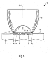
- the printed circuit board 46 is provided clearly outside the chip arrangement and surrounds it in an annular manner, as can be seen from FIG. 5. It also covers the base body 22 practically on its entire surface, so that a good thermal insulation is formed forward. Excluded from this is only a central chip area 62, which receives the chips 12 and 14. Although this circular region is shown quite generously in FIG. 5, it will be understood that instead of this, a closer approach of the printed circuit board to the chips may be favorable.
- connection surfaces 70, 72 for bonding wires 74, 76 to the outside, ie to the outer circumference of the base body 22, where they are connected via connecting wires 78, 80.
- the spacer 42 for the cover lens 40 extends annularly (see Fig. 5), wherein the cover lens 40 is in turn received in an inner shoulder 44. Between the planar rear side of the cover lens 40 and the chip area, a space 82 is formed which is bounded laterally by the annular spacer 42. This space is preferred with a transparent substance such as silicone gel or a potting compound, which may optionally have phosphor particles.
- FIG. 6 A further modified embodiment of the radiation source 10 according to the invention can be seen from FIG. 6.
- This embodiment is characterized by a likewise quite compact design, in which the LED chips are arranged in a crosswise or star-shaped manner, with nothing between the outer LED chips 14 and 20 and the optical axis 60 - except, if appropriate, a very compact reflector element 24 - extends.
- the reflector elements 24 are again formed roof-shaped, so that they reflection surfaces 26th and 28, and throw the light leaking to the side.
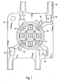
- FIG. 7 shows a total of four series resistors 84, each adjusted via laser balancing, which are assigned to the four outer LED chips 14 to 12.
- FIG. 7 shows a total of four series resistors 84, each adjusted via laser balancing, which are assigned to the four outer LED chips 14 to 12.
- it is provided to operate the central LED chip 12 with a different wavelength and independently, while the outer LED chips 14 to 20 are each connected in parallel and therefore have series resistors in their interconnects 47.
- the printed circuit board 46 is provided in the illustrated embodiment, with vias 90, which allow the terminal lugs 92 to contact from above and below.
- connecting surfaces for example the connection surfaces 70 and 72, extend from the outside next to the outer LED chips 14 to 20, while the chip region 76 remains inwardly, ie towards the optical axis, free of conductor tracks.
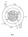
- FIGS. 8 and 9 Another embodiment is shown in FIGS. 8 and 9.
- the same or similar reference numerals indicate the same or similar part.
- five LED chips 12 to 20 are arranged substantially in a cross shape, so that the chips 14 to 20 surround a central chip 12.
- the chips are each of reflector elements 24, which extend between and adjacent to them and form part of a spacer which supports a reflector 50 in front of the LED chip.
- radiation absorbers 24 and 96 are provided which extend between the outer LED chips 14 and 20 on the one hand and the printed circuit board 46. This solution is particularly favorable when it comes to intercept high-energy radiation without affecting the printed circuit board.
- the radiation absorbers 94 and 96 may be applied as solid bodies on the base body 22, for example via an extremely thin adhesive layer, similar to the chips themselves, so that a good heat dissipation is ensured.
- the radiation absorbers 94 and 96 may be made of any suitable material.
- suitable material come, for example, Kunststoffoffoff stresses, aluminum body, but also preferably ceramic body, which may also be colored dark to ensure even better radiation absorption.
- the printed circuit board 46 is also covered by a guard ring 98, which also serves the better protection, in particular the calibration resistors, because by excessive heating of the calibration resistors, the calibration can be affected.
- guard ring 98 is dimensioned so that the connection tracks 92 remain free, wherein the guard ring is preferably configured electrically insulating at least on its underside.
- the LED chips 14, 12 and 20 are each arranged spaced from the reflector element. This also contributes to the intense heat dissipation through the LED chips not to be an intense heat application of the grating reflector 30, which may consist of plastic with mirrored surfaces.
Landscapes
- Led Device Packages (AREA)
Applications Claiming Priority (1)
| Application Number | Priority Date | Filing Date | Title |
|---|---|---|---|
| DE102006015377.4A DE102006015377B4 (de) | 2006-04-03 | 2006-04-03 | Halbleiter-Strahlungsquelle sowie Lichthärtgerät |
Publications (3)
| Publication Number | Publication Date |
|---|---|
| EP1843079A2 true EP1843079A2 (fr) | 2007-10-10 |
| EP1843079A3 EP1843079A3 (fr) | 2008-07-09 |
| EP1843079B1 EP1843079B1 (fr) | 2017-02-15 |
Family
ID=38134085
Family Applications (1)
| Application Number | Title | Priority Date | Filing Date |
|---|---|---|---|
| EP07003444.2A Active EP1843079B1 (fr) | 2006-04-03 | 2007-02-19 | Source semi-conductrice de lumière et appareil de photo-durcissement |
Country Status (5)
| Country | Link |
|---|---|
| US (1) | US20070228392A1 (fr) |
| EP (1) | EP1843079B1 (fr) |
| JP (1) | JP2007281472A (fr) |
| DE (1) | DE102006015377B4 (fr) |
| ES (1) | ES2623224T3 (fr) |
Cited By (5)
| Publication number | Priority date | Publication date | Assignee | Title |
|---|---|---|---|---|
| EP2042123A3 (fr) * | 2002-08-08 | 2009-10-07 | Kerr Corporation | Instrument lumineux de durcissement |
| US8113830B2 (en) | 2005-05-27 | 2012-02-14 | Kerr Corporation | Curing light instrument |
| US8568140B2 (en) | 1998-01-20 | 2013-10-29 | Jozef Kovac | Apparatus and method for curing materials with radiation |
| US9066777B2 (en) | 2009-04-02 | 2015-06-30 | Kerr Corporation | Curing light device |
| US9072572B2 (en) | 2009-04-02 | 2015-07-07 | Kerr Corporation | Dental light device |
Families Citing this family (19)
| Publication number | Priority date | Publication date | Assignee | Title |
|---|---|---|---|---|
| DE102007011637A1 (de) | 2007-03-09 | 2008-09-18 | Ivoclar Vivadent Ag | Lichtemissionsvorrichtung |
| DE102008005120A1 (de) * | 2008-01-18 | 2009-09-10 | Osram Gesellschaft mit beschränkter Haftung | LED-Modul mit einer Linse |
| US8097894B2 (en) * | 2009-07-23 | 2012-01-17 | Koninklijke Philips Electronics N.V. | LED with molded reflective sidewall coating |
| JP2011065979A (ja) * | 2009-08-18 | 2011-03-31 | Sharp Corp | 光源装置 |
| JP5280502B2 (ja) * | 2009-08-18 | 2013-09-04 | シャープ株式会社 | 光源装置 |
| DE102010027875A1 (de) * | 2010-04-16 | 2011-10-20 | Osram Opto Semiconductors Gmbh | Optoelektronisches Bauelement und Verfahren zum Herstellen eines optoelektronischen Bauelements |
| DE102010038396B4 (de) | 2010-07-26 | 2021-08-05 | OSRAM Opto Semiconductors Gesellschaft mit beschränkter Haftung | Optoelektronisches Bauelement und Leuchtvorrichung damit |
| DE102011107893A1 (de) * | 2011-07-18 | 2013-01-24 | Heraeus Noblelight Gmbh | Optoelektronisches Modul mit verbesserter Optik |
| US8475031B1 (en) * | 2012-01-03 | 2013-07-02 | Kocam International Co., Ltd. | LED backlight module structure for increasing process yield |
| KR102071424B1 (ko) * | 2013-01-08 | 2020-01-30 | 엘지이노텍 주식회사 | 발광소자 패키지 |
| DE202013101190U1 (de) | 2013-03-20 | 2014-06-24 | Zumtobel Lighting Gmbh | Anordnung zur Lichtabgabe mit einer LED, einer Platine und einem optischen Element |
| US10159548B2 (en) | 2014-09-17 | 2018-12-25 | Garrison Dental Solutions, L.L.C. | Dental curing light |
| KR102522590B1 (ko) * | 2016-03-25 | 2023-04-17 | 쑤저우 레킨 세미컨덕터 컴퍼니 리미티드 | 발광소자 패키지 및 조명 장치 |
| JP6952945B2 (ja) * | 2016-03-25 | 2021-10-27 | スージョウ レキン セミコンダクター カンパニー リミテッド | 発光素子パッケージ及び照明装置 |
| US10641437B2 (en) | 2016-06-30 | 2020-05-05 | Nichia Corporation | LED module |
| JP6380590B2 (ja) * | 2016-06-30 | 2018-08-29 | 日亜化学工業株式会社 | Ledモジュール |
| DE202016105841U1 (de) * | 2016-10-19 | 2018-01-22 | Tridonic Jennersdorf Gmbh | CSP LED Modul mit Reflexionsmittel |
| AU2019324038B2 (en) * | 2018-08-24 | 2022-03-24 | Tokuyama Dental Corporation | Polymerization apparatus |
| KR102442315B1 (ko) * | 2020-11-24 | 2022-09-14 | 이승훈 | 경화장치 및 이를 포함하는 머신비전 시스템 |
Family Cites Families (28)
| Publication number | Priority date | Publication date | Assignee | Title |
|---|---|---|---|---|
| JPH0717161Y2 (ja) * | 1987-07-03 | 1995-04-19 | 星和電機株式会社 | 面発光素子 |
| US5130761A (en) * | 1990-07-17 | 1992-07-14 | Kabushiki Kaisha Toshiba | Led array with reflector and printed circuit board |
| US5122943A (en) * | 1991-04-15 | 1992-06-16 | Miles Inc. | Encapsulated light emitting diode and method for encapsulation |
| JPH09298314A (ja) * | 1996-05-07 | 1997-11-18 | Nichia Chem Ind Ltd | 発光装置 |
| JPH114022A (ja) * | 1998-02-27 | 1999-01-06 | Sanyo Electric Co Ltd | 線状光源 |
| JP3656715B2 (ja) * | 1999-07-23 | 2005-06-08 | 松下電工株式会社 | 光源装置 |
| US6331111B1 (en) | 1999-09-24 | 2001-12-18 | Cao Group, Inc. | Curing light system useful for curing light activated composite materials |
| US6953340B2 (en) * | 1999-09-24 | 2005-10-11 | Cao Group, Inc. | Light for use in activating light-activated materials, the light having a detachable light module containing a heat sink and a semiconductor chip |
| JP3696020B2 (ja) | 2000-01-20 | 2005-09-14 | 三洋電機株式会社 | 混成集積回路装置 |
| GB2361581A (en) | 2000-04-20 | 2001-10-24 | Lite On Electronics Inc | A light emitting diode device |
| DE10041686A1 (de) * | 2000-08-24 | 2002-03-14 | Osram Opto Semiconductors Gmbh | Bauelement mit einer Vielzahl von Lumineszenzdiodenchips |
| JP4905751B2 (ja) * | 2001-05-17 | 2012-03-28 | 株式会社吉田製作所 | 歯科用光照射器 |
| JP4045781B2 (ja) * | 2001-08-28 | 2008-02-13 | 松下電工株式会社 | 発光装置 |
| JP4122742B2 (ja) * | 2001-08-28 | 2008-07-23 | 松下電工株式会社 | 発光装置 |
| TW578280B (en) * | 2002-11-21 | 2004-03-01 | United Epitaxy Co Ltd | Light emitting diode and package scheme and method thereof |
| WO2004068182A2 (fr) * | 2003-01-24 | 2004-08-12 | Digital Optics International Corporation | Systeme d'eclairage haute densite |
| JP2004303686A (ja) * | 2003-04-01 | 2004-10-28 | Tanimura Gangu Kenkyusho:Kk | 照明装置 |
| JP2004342870A (ja) * | 2003-05-16 | 2004-12-02 | Stanley Electric Co Ltd | 大電流駆動用発光ダイオード |
| US7391153B2 (en) * | 2003-07-17 | 2008-06-24 | Toyoda Gosei Co., Ltd. | Light emitting device provided with a submount assembly for improved thermal dissipation |
| JP2005158963A (ja) * | 2003-11-25 | 2005-06-16 | Matsushita Electric Works Ltd | 発光装置 |
| JP4255367B2 (ja) * | 2003-12-04 | 2009-04-15 | デンカAgsp株式会社 | 発光素子搭載用基板及びその製造方法 |
| WO2005067063A1 (fr) | 2004-01-12 | 2005-07-21 | Asetronics Ag | Ensemble comprenant un dispositif electroluminescent sur un substrat |
| TWI241042B (en) * | 2004-03-11 | 2005-10-01 | Chen-Lun Hsingchen | A low thermal resistance LED device |
| US20050199899A1 (en) * | 2004-03-11 | 2005-09-15 | Ming-Der Lin | Package array and package unit of flip chip LED |
| JP4492193B2 (ja) * | 2004-04-13 | 2010-06-30 | 岡谷電機産業株式会社 | 表示ランプ |
| JP2006005290A (ja) * | 2004-06-21 | 2006-01-05 | Citizen Electronics Co Ltd | 発光ダイオード |
| US20060092644A1 (en) * | 2004-10-28 | 2006-05-04 | Mok Thye L | Small package high efficiency illuminator design |
| US7655957B2 (en) * | 2006-04-27 | 2010-02-02 | Cree, Inc. | Submounts for semiconductor light emitting device packages and semiconductor light emitting device packages including the same |
-
2006
- 2006-04-03 DE DE102006015377.4A patent/DE102006015377B4/de not_active Expired - Fee Related
-
2007
- 2007-02-19 EP EP07003444.2A patent/EP1843079B1/fr active Active
- 2007-02-19 ES ES07003444.2T patent/ES2623224T3/es active Active
- 2007-03-23 US US11/728,239 patent/US20070228392A1/en not_active Abandoned
- 2007-04-03 JP JP2007097896A patent/JP2007281472A/ja active Pending
Cited By (11)
| Publication number | Priority date | Publication date | Assignee | Title |
|---|---|---|---|---|
| US8568140B2 (en) | 1998-01-20 | 2013-10-29 | Jozef Kovac | Apparatus and method for curing materials with radiation |
| US9572643B2 (en) | 1998-01-20 | 2017-02-21 | Kerr Corporation | Apparatus and method for curing materials with radiation |
| US9622839B2 (en) | 1998-01-20 | 2017-04-18 | Kerr Corporation | Apparatus and method for curing materials with radiation |
| EP2042123A3 (fr) * | 2002-08-08 | 2009-10-07 | Kerr Corporation | Instrument lumineux de durcissement |
| US8231383B2 (en) | 2002-08-08 | 2012-07-31 | Kerr Corporation | Curing light instrument |
| US8113830B2 (en) | 2005-05-27 | 2012-02-14 | Kerr Corporation | Curing light instrument |
| US9066777B2 (en) | 2009-04-02 | 2015-06-30 | Kerr Corporation | Curing light device |
| US9072572B2 (en) | 2009-04-02 | 2015-07-07 | Kerr Corporation | Dental light device |
| US9693846B2 (en) | 2009-04-02 | 2017-07-04 | Kerr Corporation | Dental light device |
| US9730778B2 (en) | 2009-04-02 | 2017-08-15 | Kerr Corporation | Curing light device |
| US9987110B2 (en) | 2009-04-02 | 2018-06-05 | Kerr Corporation | Dental light device |
Also Published As
| Publication number | Publication date |
|---|---|
| ES2623224T3 (es) | 2017-07-10 |
| JP2007281472A (ja) | 2007-10-25 |
| EP1843079A3 (fr) | 2008-07-09 |
| DE102006015377A1 (de) | 2007-10-11 |
| EP1843079B1 (fr) | 2017-02-15 |
| US20070228392A1 (en) | 2007-10-04 |
| DE102006015377B4 (de) | 2018-06-14 |
Similar Documents
| Publication | Publication Date | Title |
|---|---|---|
| EP1843079B1 (fr) | Source semi-conductrice de lumière et appareil de photo-durcissement | |
| EP1843394B1 (fr) | Source semi-conductrice de rayonnement et appareil de photodurcissement l'incorporant | |
| DE102012223854A1 (de) | Remote-Phosphor-Konvertereinrichtung | |
| DE102012101411B4 (de) | Explosionsgeschützte Leuchte mit eingegossener Optik | |
| DE102008025756B4 (de) | Halbleiteranordnung | |
| EP2989385B1 (fr) | Dispositif antidéflagrant de composants électriques et/ou électroniques | |
| EP0933823B1 (fr) | Unité d'éclairage de surface avec un dispositif semiconducteur optoélectronique compensé pour la dilatation | |
| DE2062209C3 (de) | Festkörperlampe | |
| DE19727633C2 (de) | Bauteil zur gerichteten, bidirektionalen, optischen Datenübertragung | |
| EP2583319B1 (fr) | Composant optoélectronique | |
| DE19621124A1 (de) | Optoelektronischer Wandler und dessen Herstellungsverfahren | |
| EP2735023A1 (fr) | Module optoélectronique à optique améliorée | |
| DE112004002083T5 (de) | Lichtemittierende Vorrichtung | |
| WO2015024860A1 (fr) | Diode laser se refroidissant également le long de ses faces latérales | |
| WO2013178415A1 (fr) | Lentille à couche de réflexion réfléchissant vers l'intérieur | |
| EP1968115A2 (fr) | Dispositif émetteur de lumière | |
| DE102008038748B4 (de) | Oberflächenmontierbares, optoelektronisches Halbleiterbauteil | |
| WO2012004049A1 (fr) | Diode électroluminescente | |
| EP2494271B1 (fr) | Appareil d'éclairage destiné à éclairer une zone cible au moyen d'une réflexion arrière de lumière d'un module de diode électroluminescente sur un réflecteur | |
| DE102015117539A1 (de) | Anordnung | |
| EP2327110A1 (fr) | Composant optoelectronique et son procede de production | |
| DE102016204697A1 (de) | Retrofit-Lampe und Fahrzeugscheinwerfer mit Retrofit-Lampe | |
| DE102009056779A1 (de) | Photovoltaik-Modul | |
| DE19640421A1 (de) | Optoelektronisches Modul zur bidirektionalen optischen Datenübertragung | |
| WO2014048797A2 (fr) | Module lumineux annulaire et procédé de fabrication d'un module lumineux annulaire |
Legal Events
| Date | Code | Title | Description |
|---|---|---|---|
| PUAI | Public reference made under article 153(3) epc to a published international application that has entered the european phase |
Free format text: ORIGINAL CODE: 0009012 |
|
| AK | Designated contracting states |
Kind code of ref document: A2 Designated state(s): AT BE BG CH CY CZ DE DK EE ES FI FR GB GR HU IE IS IT LI LT LU LV MC NL PL PT RO SE SI SK TR |
|
| AX | Request for extension of the european patent |
Extension state: AL BA HR MK YU |
|
| PUAL | Search report despatched |
Free format text: ORIGINAL CODE: 0009013 |
|
| AK | Designated contracting states |
Kind code of ref document: A3 Designated state(s): AT BE BG CH CY CZ DE DK EE ES FI FR GB GR HU IE IS IT LI LT LU LV MC NL PL PT RO SE SI SK TR |
|
| AX | Request for extension of the european patent |
Extension state: AL BA HR MK RS |
|
| 17P | Request for examination filed |
Effective date: 20080910 |
|
| 17Q | First examination report despatched |
Effective date: 20081023 |
|
| AKX | Designation fees paid |
Designated state(s): AT BE BG CH CY CZ DE DK EE ES FI FR GB GR HU IE IS IT LI LT LU LV MC NL PL PT RO SE SI SK TR |
|
| REG | Reference to a national code |
Ref country code: DE Ref legal event code: R079 Ref document number: 502007015439 Country of ref document: DE Free format text: PREVIOUS MAIN CLASS: F21K0007000000 Ipc: H01L0025075000 |
|
| GRAP | Despatch of communication of intention to grant a patent |
Free format text: ORIGINAL CODE: EPIDOSNIGR1 |
|
| RIC1 | Information provided on ipc code assigned before grant |
Ipc: H01L 33/64 20100101ALN20160901BHEP Ipc: H01L 33/60 20100101ALN20160901BHEP Ipc: H01L 25/075 20060101AFI20160901BHEP Ipc: A61C 13/15 20060101ALN20160901BHEP |
|
| INTG | Intention to grant announced |
Effective date: 20160915 |
|
| GRAS | Grant fee paid |
Free format text: ORIGINAL CODE: EPIDOSNIGR3 |
|
| GRAA | (expected) grant |
Free format text: ORIGINAL CODE: 0009210 |
|
| AK | Designated contracting states |
Kind code of ref document: B1 Designated state(s): AT BE BG CH CY CZ DE DK EE ES FI FR GB GR HU IE IS IT LI LT LU LV MC NL PL PT RO SE SI SK TR |
|
| REG | Reference to a national code |
Ref country code: CH Ref legal event code: EP Ref country code: GB Ref legal event code: FG4D Free format text: NOT ENGLISH |
|
| REG | Reference to a national code |
Ref country code: FR Ref legal event code: PLFP Year of fee payment: 11 |
|
| REG | Reference to a national code |
Ref country code: CH Ref legal event code: NV Representative=s name: KELLER AND PARTNER PATENTANWAELTE AG, CH |
|
| REG | Reference to a national code |
Ref country code: IE Ref legal event code: FG4D Free format text: LANGUAGE OF EP DOCUMENT: GERMAN |
|
| REG | Reference to a national code |
Ref country code: AT Ref legal event code: REF Ref document number: 868321 Country of ref document: AT Kind code of ref document: T Effective date: 20170315 |
|
| REG | Reference to a national code |
Ref country code: DE Ref legal event code: R096 Ref document number: 502007015439 Country of ref document: DE |
|
| REG | Reference to a national code |
Ref country code: SE Ref legal event code: TRGR |
|
| REG | Reference to a national code |
Ref country code: NL Ref legal event code: MP Effective date: 20170215 |
|
| REG | Reference to a national code |
Ref country code: LT Ref legal event code: MG4D |
|
| REG | Reference to a national code |
Ref country code: ES Ref legal event code: FG2A Ref document number: 2623224 Country of ref document: ES Kind code of ref document: T3 Effective date: 20170710 |
|
| PG25 | Lapsed in a contracting state [announced via postgrant information from national office to epo] |
Ref country code: FI Free format text: LAPSE BECAUSE OF FAILURE TO SUBMIT A TRANSLATION OF THE DESCRIPTION OR TO PAY THE FEE WITHIN THE PRESCRIBED TIME-LIMIT Effective date: 20170215 Ref country code: LT Free format text: LAPSE BECAUSE OF FAILURE TO SUBMIT A TRANSLATION OF THE DESCRIPTION OR TO PAY THE FEE WITHIN THE PRESCRIBED TIME-LIMIT Effective date: 20170215 Ref country code: GR Free format text: LAPSE BECAUSE OF FAILURE TO SUBMIT A TRANSLATION OF THE DESCRIPTION OR TO PAY THE FEE WITHIN THE PRESCRIBED TIME-LIMIT Effective date: 20170516 |
|
| PG25 | Lapsed in a contracting state [announced via postgrant information from national office to epo] |
Ref country code: PT Free format text: LAPSE BECAUSE OF FAILURE TO SUBMIT A TRANSLATION OF THE DESCRIPTION OR TO PAY THE FEE WITHIN THE PRESCRIBED TIME-LIMIT Effective date: 20170615 Ref country code: LV Free format text: LAPSE BECAUSE OF FAILURE TO SUBMIT A TRANSLATION OF THE DESCRIPTION OR TO PAY THE FEE WITHIN THE PRESCRIBED TIME-LIMIT Effective date: 20170215 Ref country code: BG Free format text: LAPSE BECAUSE OF FAILURE TO SUBMIT A TRANSLATION OF THE DESCRIPTION OR TO PAY THE FEE WITHIN THE PRESCRIBED TIME-LIMIT Effective date: 20170515 Ref country code: NL Free format text: LAPSE BECAUSE OF FAILURE TO SUBMIT A TRANSLATION OF THE DESCRIPTION OR TO PAY THE FEE WITHIN THE PRESCRIBED TIME-LIMIT Effective date: 20170215 |
|
| PG25 | Lapsed in a contracting state [announced via postgrant information from national office to epo] |
Ref country code: EE Free format text: LAPSE BECAUSE OF FAILURE TO SUBMIT A TRANSLATION OF THE DESCRIPTION OR TO PAY THE FEE WITHIN THE PRESCRIBED TIME-LIMIT Effective date: 20170215 Ref country code: SK Free format text: LAPSE BECAUSE OF FAILURE TO SUBMIT A TRANSLATION OF THE DESCRIPTION OR TO PAY THE FEE WITHIN THE PRESCRIBED TIME-LIMIT Effective date: 20170215 Ref country code: RO Free format text: LAPSE BECAUSE OF FAILURE TO SUBMIT A TRANSLATION OF THE DESCRIPTION OR TO PAY THE FEE WITHIN THE PRESCRIBED TIME-LIMIT Effective date: 20170215 Ref country code: CZ Free format text: LAPSE BECAUSE OF FAILURE TO SUBMIT A TRANSLATION OF THE DESCRIPTION OR TO PAY THE FEE WITHIN THE PRESCRIBED TIME-LIMIT Effective date: 20170215 |
|
| REG | Reference to a national code |
Ref country code: DE Ref legal event code: R097 Ref document number: 502007015439 Country of ref document: DE |
|
| REG | Reference to a national code |
Ref country code: IE Ref legal event code: MM4A |
|
| PG25 | Lapsed in a contracting state [announced via postgrant information from national office to epo] |
Ref country code: DK Free format text: LAPSE BECAUSE OF FAILURE TO SUBMIT A TRANSLATION OF THE DESCRIPTION OR TO PAY THE FEE WITHIN THE PRESCRIBED TIME-LIMIT Effective date: 20170215 Ref country code: MC Free format text: LAPSE BECAUSE OF FAILURE TO SUBMIT A TRANSLATION OF THE DESCRIPTION OR TO PAY THE FEE WITHIN THE PRESCRIBED TIME-LIMIT Effective date: 20170215 Ref country code: PL Free format text: LAPSE BECAUSE OF FAILURE TO SUBMIT A TRANSLATION OF THE DESCRIPTION OR TO PAY THE FEE WITHIN THE PRESCRIBED TIME-LIMIT Effective date: 20170215 |
|
| PLBE | No opposition filed within time limit |
Free format text: ORIGINAL CODE: 0009261 |
|
| STAA | Information on the status of an ep patent application or granted ep patent |
Free format text: STATUS: NO OPPOSITION FILED WITHIN TIME LIMIT |
|
| PG25 | Lapsed in a contracting state [announced via postgrant information from national office to epo] |
Ref country code: LU Free format text: LAPSE BECAUSE OF NON-PAYMENT OF DUE FEES Effective date: 20170219 |
|
| 26N | No opposition filed |
Effective date: 20171116 |
|
| REG | Reference to a national code |
Ref country code: BE Ref legal event code: MM Effective date: 20170228 |
|
| REG | Reference to a national code |
Ref country code: FR Ref legal event code: PLFP Year of fee payment: 12 |
|
| PG25 | Lapsed in a contracting state [announced via postgrant information from national office to epo] |
Ref country code: IE Free format text: LAPSE BECAUSE OF NON-PAYMENT OF DUE FEES Effective date: 20170219 Ref country code: SI Free format text: LAPSE BECAUSE OF FAILURE TO SUBMIT A TRANSLATION OF THE DESCRIPTION OR TO PAY THE FEE WITHIN THE PRESCRIBED TIME-LIMIT Effective date: 20170215 |
|
| PG25 | Lapsed in a contracting state [announced via postgrant information from national office to epo] |
Ref country code: BE Free format text: LAPSE BECAUSE OF NON-PAYMENT OF DUE FEES Effective date: 20170228 |
|
| PG25 | Lapsed in a contracting state [announced via postgrant information from national office to epo] |
Ref country code: HU Free format text: LAPSE BECAUSE OF FAILURE TO SUBMIT A TRANSLATION OF THE DESCRIPTION OR TO PAY THE FEE WITHIN THE PRESCRIBED TIME-LIMIT; INVALID AB INITIO Effective date: 20070219 |
|
| PG25 | Lapsed in a contracting state [announced via postgrant information from national office to epo] |
Ref country code: CY Free format text: LAPSE BECAUSE OF NON-PAYMENT OF DUE FEES Effective date: 20170215 |
|
| PG25 | Lapsed in a contracting state [announced via postgrant information from national office to epo] |
Ref country code: TR Free format text: LAPSE BECAUSE OF FAILURE TO SUBMIT A TRANSLATION OF THE DESCRIPTION OR TO PAY THE FEE WITHIN THE PRESCRIBED TIME-LIMIT Effective date: 20170215 |
|
| PG25 | Lapsed in a contracting state [announced via postgrant information from national office to epo] |
Ref country code: IS Free format text: LAPSE BECAUSE OF FAILURE TO SUBMIT A TRANSLATION OF THE DESCRIPTION OR TO PAY THE FEE WITHIN THE PRESCRIBED TIME-LIMIT Effective date: 20170615 |
|
| REG | Reference to a national code |
Ref country code: CH Ref legal event code: PFA Owner name: IVOCLAR VIVADENT AG, LI Free format text: FORMER OWNER: IVOCLAR VIVADENT AG, LI |
|
| P01 | Opt-out of the competence of the unified patent court (upc) registered |
Effective date: 20230607 |
|
| REG | Reference to a national code |
Ref country code: DE Ref legal event code: R079 Ref document number: 502007015439 Country of ref document: DE Free format text: PREVIOUS MAIN CLASS: H01L0025075000 Ipc: H10H0029240000 |
|
| PGFP | Annual fee paid to national office [announced via postgrant information from national office to epo] |
Ref country code: DE Payment date: 20250220 Year of fee payment: 19 |
|
| PGFP | Annual fee paid to national office [announced via postgrant information from national office to epo] |
Ref country code: ES Payment date: 20250306 Year of fee payment: 19 |
|
| PGFP | Annual fee paid to national office [announced via postgrant information from national office to epo] |
Ref country code: SE Payment date: 20250225 Year of fee payment: 19 |
|
| PGFP | Annual fee paid to national office [announced via postgrant information from national office to epo] |
Ref country code: AT Payment date: 20250221 Year of fee payment: 19 Ref country code: CH Payment date: 20250319 Year of fee payment: 19 |
|
| PGFP | Annual fee paid to national office [announced via postgrant information from national office to epo] |
Ref country code: GB Payment date: 20250225 Year of fee payment: 19 Ref country code: IT Payment date: 20250108 Year of fee payment: 19 |
|
| PGFP | Annual fee paid to national office [announced via postgrant information from national office to epo] |
Ref country code: FR Payment date: 20260225 Year of fee payment: 20 |