EP1843080A2 - Source de rayonnement semi-conductrice - Google Patents
Source de rayonnement semi-conductrice Download PDFInfo
- Publication number
- EP1843080A2 EP1843080A2 EP07004128A EP07004128A EP1843080A2 EP 1843080 A2 EP1843080 A2 EP 1843080A2 EP 07004128 A EP07004128 A EP 07004128A EP 07004128 A EP07004128 A EP 07004128A EP 1843080 A2 EP1843080 A2 EP 1843080A2
- Authority
- EP
- European Patent Office
- Prior art keywords
- radiation source
- source according
- led chips
- base body
- light
- Prior art date
- Legal status (The legal status is an assumption and is not a legal conclusion. Google has not performed a legal analysis and makes no representation as to the accuracy of the status listed.)
- Withdrawn
Links
Images

Classifications
-
- H—ELECTRICITY
- H10—SEMICONDUCTOR DEVICES; ELECTRIC SOLID-STATE DEVICES NOT OTHERWISE PROVIDED FOR
- H10W—GENERIC PACKAGES, INTERCONNECTIONS, CONNECTORS OR OTHER CONSTRUCTIONAL DETAILS OF DEVICES COVERED BY CLASS H10
- H10W90/00—Package configurations
-
- A—HUMAN NECESSITIES
- A61—MEDICAL OR VETERINARY SCIENCE; HYGIENE
- A61C—DENTISTRY; APPARATUS OR METHODS FOR ORAL OR DENTAL HYGIENE
- A61C19/00—Dental auxiliary appliances
- A61C19/003—Apparatus for curing resins by radiation
- A61C19/004—Hand-held apparatus, e.g. guns
-
- A—HUMAN NECESSITIES
- A61—MEDICAL OR VETERINARY SCIENCE; HYGIENE
- A61N—ELECTROTHERAPY; MAGNETOTHERAPY; RADIATION THERAPY; ULTRASOUND THERAPY
- A61N5/00—Radiation therapy
- A61N5/06—Radiation therapy using light
- A61N2005/065—Light sources therefor
- A61N2005/0651—Diodes
- A61N2005/0652—Arrays of diodes
-
- F—MECHANICAL ENGINEERING; LIGHTING; HEATING; WEAPONS; BLASTING
- F21—LIGHTING
- F21K—NON-ELECTRIC LIGHT SOURCES USING LUMINESCENCE; LIGHT SOURCES USING ELECTROCHEMILUMINESCENCE; LIGHT SOURCES USING CHARGES OF COMBUSTIBLE MATERIAL; LIGHT SOURCES USING SEMICONDUCTOR DEVICES AS LIGHT-GENERATING ELEMENTS; LIGHT SOURCES NOT OTHERWISE PROVIDED FOR
- F21K9/00—Light sources using semiconductor devices as light-generating elements, e.g. using light-emitting diodes [LED] or lasers
-
- Y—GENERAL TAGGING OF NEW TECHNOLOGICAL DEVELOPMENTS; GENERAL TAGGING OF CROSS-SECTIONAL TECHNOLOGIES SPANNING OVER SEVERAL SECTIONS OF THE IPC; TECHNICAL SUBJECTS COVERED BY FORMER USPC CROSS-REFERENCE ART COLLECTIONS [XRACs] AND DIGESTS
- Y10—TECHNICAL SUBJECTS COVERED BY FORMER USPC
- Y10S—TECHNICAL SUBJECTS COVERED BY FORMER USPC CROSS-REFERENCE ART COLLECTIONS [XRACs] AND DIGESTS
- Y10S362/00—Illumination
- Y10S362/80—Light emitting diode
-
- Y—GENERAL TAGGING OF NEW TECHNOLOGICAL DEVELOPMENTS; GENERAL TAGGING OF CROSS-SECTIONAL TECHNOLOGIES SPANNING OVER SEVERAL SECTIONS OF THE IPC; TECHNICAL SUBJECTS COVERED BY FORMER USPC CROSS-REFERENCE ART COLLECTIONS [XRACs] AND DIGESTS
- Y10—TECHNICAL SUBJECTS COVERED BY FORMER USPC
- Y10S—TECHNICAL SUBJECTS COVERED BY FORMER USPC CROSS-REFERENCE ART COLLECTIONS [XRACs] AND DIGESTS
- Y10S362/00—Illumination
- Y10S362/804—Surgical or dental spotlight
Definitions
- the invention relates to a semiconductor radiation source, according to the preamble of claim 1, a light curing apparatus according to the preamble of claim 21 and a lighting apparatus according to the preamble of claim 24.
- the LEDs are bundled and are supplied with power evenly, so that a selective control is not possible. Different photoinitiators with different spectral sensitivity can not be accommodated with this solution.
- the invention has for its object to provide a radiation source according to the preamble of claim 1, which is universally applicable, is relatively inexpensive to manufacture, but still allows a good radiation yield.
- the light sources are divided into two light sources, wherein both light sources, which may each consist of a plurality of LED chips, are arranged in a central region of a common base body.
- the light sources occupy only a very small part - for example 10% or 15% or even only 5% - of the surface of the base body.
- the first light source is arranged in an optical axis and the second light source has at least two LED chips which, in particular symmetrical to one another and surrounding the optical axis and the optical axis, are arranged.
- a first light source is disposed in the optical axis and a second light source is surrounding and closely adjacent thereto.
- the second light source is preferably arranged symmetrically, it being understood that at least two LED chips are required for this symmetrical arrangement.
- the first light source as a central LED chip and the four LED chips of the second light source, which then surround the LED chip of the first light source.
- any suitable means can be used, that is, for example, a cover lens which covers the LED chips and bundles the emerging light, as well as possibly a converging lens, which further focusses allows the emitted light radiation.
- photoinitiators in light-curing compositions can be excited in any suitable manner by dividing the light output into two light sources.
- the first light source may be designed to excite lucerin in the wavelength range of 400 to 430 nm and the second light source to excite camphorquinone for the wavelength range between 450 and 480 nm.
- both light sources can be switched on together, while depending on the material used, each light source can be switched on separately.
- the radiation source according to the invention can be used multifunctional, that is not only as a light curing device, but also as a lighting device, in particular for the examination of whether there are dental gaps in existing plastic fillings in the patient's mouth or not.
- a hand-held device which is shaped in the manner of a handheld light curing device, particularly well suited, because the light source can be introduced directly into the mouth of the patient through the most solid light guide and the slim shape and there the lighting are made glare-free.
- the test wavelength can be adapted to the requirements in a wide range; it is preferably the shorter wavelength emitted by the first light source located in the optical axis.
- the second light source has four LED chips, which are arranged in the manner of a cross around the first light source, and that the first light source has an LED chip.
- the light sources adjoin one another closely, the width of the gap remaining between them being less than one fifth, in particular approximately one tenth, of the diameter of each LED chip.
- the gap width is preferably 0.5 to 2 mm and in particular about 1 mm.
- the first and the second light source are arranged in a central region of the base body.
- At least the first light source in particular all light sources are arranged on a central projection, in particular with a height between 0.1 and 1 mm, of the base body.
- the projection follows in its shape the light sources and in particular has substantially the shape of a cross.
- the light sources are fixed on the base body or the projection by an adhesive bond or by a solder joint.
- the base body and / or the projection has a thermal conductivity which is better than 0.5 ° C / W.
- the base body and / or the projection is electrically conductive.
- the base body consists at least partially of copper.
- the base body is at least partially coated with gold or nickel-gold.
- a central region, in particular the projection, the base body surrounding a printed circuit board is arranged, which carries electrical connection contacts.
- electrical connection contacts for the light sources are arranged as fields on the outer circumference of the base body, in particular on a printed circuit board, and that bonding wires extend from the LED chips to the electrical connection contacts.
- the light sources are covered by a convex cover lens, which is in particular formed flat on the side facing the light sources.
- a spacer which is supported in particular on the printed circuit board, surrounds the light sources and that the spacer forms a closed space in front of the light sources, in particular together with the cover lens.
- the closed space has a liquid or viscous substance, in particular silicone gel, or a potting compound.
- an optical element which extends in front of the light sources in particular the cover lens or a mass which extends in front of the light sources, has phosphor particles.
- a collecting lens is arranged in front of the light sources, spaced a multiple of their diameter, in particular in front of the cover lens.
- the cover lens has a significantly larger diameter than the light sources and a converging lens has a significantly larger diameter than the cover lens, the diameter ratios are each in particular between 1.2: 1 and 10: 1.
- an optical waveguide is arranged in the optical axis of the semiconductor radiation source, in particular in the radiation direction after the converging lens.
- the first and second light sources can be switched on together.
- the first and second light source can be switched on or off at different times.
- Fig. 1 shows a semiconductor radiation source 10 in a schematic plan view.
- a base body 12 is provided which carries two LED chips in a central region 14.
- a first light source 16 is provided, which is arranged in an optical axis.
- Both light sources 16 and 18 are arranged in this embodiment directly in the central region of the base body 12 on which they are mounted, and at the same time serves to dissipate the heat generated by the LED chips.
- the two LED chips are each disposed immediately adjacent to the optical axis 22. They have a gap 20 between them, which is kept as low as it is technically and electrically possible to avoid short circuits, the distance may be a few micrometers.
- Each LED chip is square in a conventional manner.
- FIG. 2 shows a further embodiment of the semiconductor radiation source 10 according to the invention.
- the first light source 16 is provided directly in the optical axis 22.
- the second light source 18 consists of four LED chips 24, 26, 28 and 30, which are arranged in a cross shape around the LED chip of the first light source 18 around. All chips have the same dimensions, so that the edge lengths correspond to each other. In turn, very narrow gaps 20 are provided which allow electrical separation, but do not affect the spatial proximity of all LED chips in the central region 14.
- first and the second light source 16 and 18 are independently switchable and occupy the central region 14 of the base body 12, wherein a much larger area remains free.
- FIG. 3 shows a further embodiment of a radiation source 10 according to the invention.
- a projection 31 is provided, which carries the first and the second light source 16 and 18.
- the projection 31 follows in its shape the cross formed by the first and second light sources 16 and 18, wherein the transitions of the legs at 32 per radius and thus are somewhat rounded and enlarged. This allows a simplified assembly and a good heat dissipation of the LED chips on the base body 10th
- the base body 10 preferably consists essentially of copper and is in particular coated on its front side, ie adjacent to the light sources, with a nickel-gold layer. In a modified embodiment, the base body is completely coated externally with this layer.
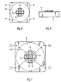
- the base body 12 has a chamfer 34 at a corner.
- the chamfer 34 is used to facilitate assembly, so as to ensure that the discussed with reference to the following figures contact surfaces are switched correctly.
- the thickness of the LED chips is substantially less than the thickness of the base body, for example by a factor of 10.
- the strength of the LED chips for the light sources 16 and 18 is also slightly less than the height of the projection 31.
- the central region 14 can be surrounded by an annular surface 40, which is preferably formed by a printed circuit board 41 resting on the base body 12.
- an annular surface 40 which is preferably formed by a printed circuit board 41 resting on the base body 12.
- a circular ring is formed, which is fitted into the substantially square shape of the base body 12.
- the contact fields 42 to 48 are used to make contact with connecting wires or bonding wires for the LED chips of the light sources 16, 18. Accordingly, the bonding wires (see also Fig. 7) extend beyond the annular surface 40. This also benefits the concentration of the light output on the really important central area 14.
- the printed circuit board 41 can extend substantially the same height as the projection 31. It is understood that in any way a height adjustment can be made so that the printed circuit board or the projection can be thicker.
- series resistors are additionally provided for the LED chips. With these series resistors can be carried out in parallel connection of LED chips calibration, so that even unsorted LED chips that are inexpensive, can be used.
- the electrical insulation of the LED chips 24 to 30 and the LED chip of the light source 16 can be realized in a conventional manner, for example, by a corresponding oxidation layer of the semiconductor material used. This is not precluded that the LED chips can be securely fixed to the projection 31 or the base body 12.
- a spacer 40 can surround the central region 14.
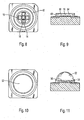
- the spacer 40 may be formed of plastic or light metal, for example, and protect the light sources 16 and 18. In the illustrated embodiment, it is annular and is provided for receiving the apparent from Fig. 10 and 11 cover lens 52.
- this space 54 is closed and filled with a special substance.
- this silicone gel 56 is provided, which is provided with yellow phosphor particles. This ensures that the emitted light receives a higher proportion of white, without the light output would be significantly affected.
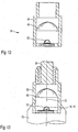
- the radiation source according to the invention is installed in a partially illustrated combined illumination and light curing device.
- a converging lens 60 is provided, which is mounted via an optical holder 62 so that it extends above the cover lens 52 and although this overlapping and covering.
- a light guide 64 extends in the direction of radiation subsequent to the converging lens 60.
- the light curing device has, as it is schematically indicated in Fig. 13, a housing 70 and is designed as a handheld device.
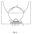
- both the light sources 16, 18 and the cover lens 52, but also the converging lens 60 and the light guide 64 along the optical axis 22 are arranged. This allows a particularly good yield and easy focus on the desired focus.
Landscapes
- Non-Portable Lighting Devices Or Systems Thereof (AREA)
- Led Device Packages (AREA)
- Semiconductor Lasers (AREA)
Applications Claiming Priority (1)
| Application Number | Priority Date | Filing Date | Title |
|---|---|---|---|
| DE200610015336 DE102006015336B4 (de) | 2006-04-03 | 2006-04-03 | Halbleiter-Strahlungsquelle, Lichthärtgerät mit Halbleiter-Strahlungsquelle, Beleuchtungsgerät mit Halbleiter-Strahlungsquelle und Verwendung eines Beleuchtungsgeräts mit Halbleiter-Strahlungsquelle |
Publications (2)
| Publication Number | Publication Date |
|---|---|
| EP1843080A2 true EP1843080A2 (fr) | 2007-10-10 |
| EP1843080A3 EP1843080A3 (fr) | 2008-07-16 |
Family
ID=38134083
Family Applications (1)
| Application Number | Title | Priority Date | Filing Date |
|---|---|---|---|
| EP07004128A Withdrawn EP1843080A3 (fr) | 2006-04-03 | 2007-02-28 | Source de rayonnement semi-conductrice |
Country Status (4)
| Country | Link |
|---|---|
| US (1) | US7530707B2 (fr) |
| EP (1) | EP1843080A3 (fr) |
| JP (1) | JP5049041B2 (fr) |
| DE (1) | DE102006015336B4 (fr) |
Cited By (1)
| Publication number | Priority date | Publication date | Assignee | Title |
|---|---|---|---|---|
| EP2058580A1 (fr) * | 2007-11-10 | 2009-05-13 | Chuntlon Enterprise Co., Ltd. | Lampe DEL à fort éclairage et faible consommation électrique |
Families Citing this family (11)
| Publication number | Priority date | Publication date | Assignee | Title |
|---|---|---|---|---|
| US6200134B1 (en) | 1998-01-20 | 2001-03-13 | Kerr Corporation | Apparatus and method for curing materials with radiation |
| US7182597B2 (en) | 2002-08-08 | 2007-02-27 | Kerr Corporation | Curing light instrument |
| US8113830B2 (en) | 2005-05-27 | 2012-02-14 | Kerr Corporation | Curing light instrument |
| DE102006015336B4 (de) * | 2006-04-03 | 2015-05-07 | Ivoclar Vivadent Ag | Halbleiter-Strahlungsquelle, Lichthärtgerät mit Halbleiter-Strahlungsquelle, Beleuchtungsgerät mit Halbleiter-Strahlungsquelle und Verwendung eines Beleuchtungsgeräts mit Halbleiter-Strahlungsquelle |
| US9066777B2 (en) | 2009-04-02 | 2015-06-30 | Kerr Corporation | Curing light device |
| US9072572B2 (en) | 2009-04-02 | 2015-07-07 | Kerr Corporation | Dental light device |
| CN101718400A (zh) * | 2009-12-11 | 2010-06-02 | 深圳市众明半导体照明有限公司 | 一种大角度led照明装置 |
| EP2620691B1 (fr) * | 2012-01-26 | 2015-07-08 | Panasonic Corporation | Dispositif d'éclairage |
| US10159548B2 (en) | 2014-09-17 | 2018-12-25 | Garrison Dental Solutions, L.L.C. | Dental curing light |
| EP3173062A1 (fr) * | 2015-11-30 | 2017-05-31 | Philipps-Universität Marburg | Lampe de polymerisation et composite de remplissage de cavites dentaires |
| CN112823762A (zh) * | 2019-11-21 | 2021-05-21 | 深圳市天耀光电有限公司 | 一种宽谱光固化灯珠及其出光融合方法、及牙科光固化机 |
Citations (3)
| Publication number | Priority date | Publication date | Assignee | Title |
|---|---|---|---|---|
| US20030053310A1 (en) * | 2001-09-17 | 2003-03-20 | Matthew Sommers | Variable optics spot module |
| DE10144414A1 (de) * | 2001-09-10 | 2003-03-27 | Ivoclar Vivadent Ag | Lichthärtgerät |
| EP1439412A1 (fr) * | 2003-01-14 | 2004-07-21 | Eastman Kodak Company | Structure multicône pour matrice de DEL |
Family Cites Families (26)
| Publication number | Priority date | Publication date | Assignee | Title |
|---|---|---|---|---|
| DE3404904C2 (de) | 1984-02-11 | 1986-01-16 | Kulzer & Co GmbH, 6393 Wehrheim | Verfahren zur Herstellung von kieferorthopädischen Geräten und Apparaturen |
| JPS6239081A (ja) * | 1985-08-13 | 1987-02-20 | Sharp Corp | 発光半導体装置 |
| GB8522246D0 (en) * | 1985-09-07 | 1985-10-09 | Marl International Ltd | Light indicator |
| JPH0717161Y2 (ja) * | 1987-07-03 | 1995-04-19 | 星和電機株式会社 | 面発光素子 |
| JPH09298314A (ja) * | 1996-05-07 | 1997-11-18 | Nichia Chem Ind Ltd | 発光装置 |
| DE19721311C1 (de) * | 1997-05-21 | 1998-12-03 | Eka Ges Fuer Medizinisch Tech | Bestrahlungsgerät zur Polymerisation von lichthärtenden Kunststoffen |
| US6200134B1 (en) * | 1998-01-20 | 2001-03-13 | Kerr Corporation | Apparatus and method for curing materials with radiation |
| JPH114022A (ja) * | 1998-02-27 | 1999-01-06 | Sanyo Electric Co Ltd | 線状光源 |
| US6439888B1 (en) * | 1999-05-03 | 2002-08-27 | Pls Liquidating Llc | Optical source and method |
| JP3656715B2 (ja) * | 1999-07-23 | 2005-06-08 | 松下電工株式会社 | 光源装置 |
| US6953340B2 (en) * | 1999-09-24 | 2005-10-11 | Cao Group, Inc. | Light for use in activating light-activated materials, the light having a detachable light module containing a heat sink and a semiconductor chip |
| JP2001345485A (ja) * | 2000-06-02 | 2001-12-14 | Toyoda Gosei Co Ltd | 発光装置 |
| JP4905751B2 (ja) * | 2001-05-17 | 2012-03-28 | 株式会社吉田製作所 | 歯科用光照射器 |
| US6866506B2 (en) | 2001-05-23 | 2005-03-15 | Ivoclar Vivadent Ag | Light hardening apparatus particularly for a dental practice |
| DE10125340B4 (de) * | 2001-05-23 | 2004-08-05 | Ivoclar Vivadent Ag | Dentales Lichtgerät |
| JP4045781B2 (ja) * | 2001-08-28 | 2008-02-13 | 松下電工株式会社 | 発光装置 |
| JP4122742B2 (ja) * | 2001-08-28 | 2008-07-23 | 松下電工株式会社 | 発光装置 |
| JP2004128444A (ja) * | 2002-07-31 | 2004-04-22 | Shin Etsu Handotai Co Ltd | 発光素子及びそれを用いた照明装置 |
| JP2004303686A (ja) * | 2003-04-01 | 2004-10-28 | Tanimura Gangu Kenkyusho:Kk | 照明装置 |
| EP1676076A2 (fr) * | 2003-08-29 | 2006-07-05 | Koninklijke Philips Electronics N.V. | Systeme d'eclairage a melange de couleurs |
| JP2005158963A (ja) * | 2003-11-25 | 2005-06-16 | Matsushita Electric Works Ltd | 発光装置 |
| JP4492193B2 (ja) * | 2004-04-13 | 2010-06-30 | 岡谷電機産業株式会社 | 表示ランプ |
| JP2006005290A (ja) * | 2004-06-21 | 2006-01-05 | Citizen Electronics Co Ltd | 発光ダイオード |
| WO2006014364A2 (fr) * | 2004-07-02 | 2006-02-09 | Discus Dental Impressions, Inc. | Lumiere de durcissement a pointe detachable |
| TWI253191B (en) * | 2005-01-06 | 2006-04-11 | Genesis Photonics Inc | White light-emitting equipment with LED, and its application |
| DE102006015336B4 (de) * | 2006-04-03 | 2015-05-07 | Ivoclar Vivadent Ag | Halbleiter-Strahlungsquelle, Lichthärtgerät mit Halbleiter-Strahlungsquelle, Beleuchtungsgerät mit Halbleiter-Strahlungsquelle und Verwendung eines Beleuchtungsgeräts mit Halbleiter-Strahlungsquelle |
-
2006
- 2006-04-03 DE DE200610015336 patent/DE102006015336B4/de not_active Expired - Fee Related
-
2007
- 2007-02-28 EP EP07004128A patent/EP1843080A3/fr not_active Withdrawn
- 2007-03-23 US US11/728,251 patent/US7530707B2/en active Active
- 2007-04-03 JP JP2007097897A patent/JP5049041B2/ja not_active Expired - Fee Related
Patent Citations (3)
| Publication number | Priority date | Publication date | Assignee | Title |
|---|---|---|---|---|
| DE10144414A1 (de) * | 2001-09-10 | 2003-03-27 | Ivoclar Vivadent Ag | Lichthärtgerät |
| US20030053310A1 (en) * | 2001-09-17 | 2003-03-20 | Matthew Sommers | Variable optics spot module |
| EP1439412A1 (fr) * | 2003-01-14 | 2004-07-21 | Eastman Kodak Company | Structure multicône pour matrice de DEL |
Cited By (1)
| Publication number | Priority date | Publication date | Assignee | Title |
|---|---|---|---|---|
| EP2058580A1 (fr) * | 2007-11-10 | 2009-05-13 | Chuntlon Enterprise Co., Ltd. | Lampe DEL à fort éclairage et faible consommation électrique |
Also Published As
| Publication number | Publication date |
|---|---|
| EP1843080A3 (fr) | 2008-07-16 |
| US7530707B2 (en) | 2009-05-12 |
| DE102006015336B4 (de) | 2015-05-07 |
| JP2007281473A (ja) | 2007-10-25 |
| US20070230208A1 (en) | 2007-10-04 |
| DE102006015336A1 (de) | 2007-10-11 |
| JP5049041B2 (ja) | 2012-10-17 |
Similar Documents
| Publication | Publication Date | Title |
|---|---|---|
| EP1843080A2 (fr) | Source de rayonnement semi-conductrice | |
| EP1352432B9 (fr) | Diode luminescente et procede permettant de la produire | |
| DE102012102114B4 (de) | Strahlungsemittierendes Halbleiterbauteil, Beleuchtungsvorrichtung und Anzeigevorrichtung | |
| EP2287925B1 (fr) | Dispositif semiconducteur optoélectronique compensé pour la dilatation, en particulier diode émettant dans l'UV | |
| EP1843394B1 (fr) | Source semi-conductrice de rayonnement et appareil de photodurcissement l'incorporant | |
| EP2583319B1 (fr) | Composant optoélectronique | |
| EP1260196B1 (fr) | Dispositif d'éclairage | |
| WO2003049204A2 (fr) | Composant optoelectronique | |
| EP1925035A1 (fr) | Composant optoelectronique | |
| EP1004145A1 (fr) | Composant optoelectronique | |
| DE102005008775A1 (de) | Lichtemittierende Vorrichtung und Beleuchtungs-Vorrichtung | |
| EP0879582A2 (fr) | Appareil à rayonnement pour la polymérisation de résines | |
| EP2218118A1 (fr) | Ensemble muni d'au moins un composant semi-conducteur optoélectronique | |
| EP1794817B1 (fr) | Composant optoelectronique et boitier pour composant optoelectronique | |
| DE102006061118A1 (de) | Licht aussendende Vorrichtung, Verfahren zu deren Herstellung und Baugruppe | |
| DE102009007650A1 (de) | Beleuchtungsmittel mit Wärmespreizung durch Wärmeleitbeschichtung und Anpassung an das Stromversorgungsnetz und Herstellungsverfahren hierfür | |
| DE10104579A1 (de) | Lichthärtgerät | |
| WO2010025701A1 (fr) | Composant optoélectronique et son procédé de production | |
| EP1627455A2 (fr) | Procede de production d'un composant a diodes laser, boitier pour composant a diodes laser, et composant a diodes laser y relatif | |
| EP2486604B1 (fr) | Mise en contact d'un composant semi-conducteur optoélectronique par un élément de conversion | |
| WO2018146084A1 (fr) | Unité à led | |
| DE102014205470B4 (de) | Leuchtvorrichtung mit CoB-Bereich | |
| DE102013204293A1 (de) | Herstellung eines optoelektronischen Bauelements | |
| EP1260193A2 (fr) | Dispositif d'éclairage dentaire | |
| DE102011113963A1 (de) | Optoelektronisches Halbleiterbauelement |
Legal Events
| Date | Code | Title | Description |
|---|---|---|---|
| PUAI | Public reference made under article 153(3) epc to a published international application that has entered the european phase |
Free format text: ORIGINAL CODE: 0009012 |
|
| AK | Designated contracting states |
Kind code of ref document: A2 Designated state(s): AT BE BG CH CY CZ DE DK EE ES FI FR GB GR HU IE IS IT LI LT LU LV MC NL PL PT RO SE SI SK TR |
|
| AX | Request for extension of the european patent |
Extension state: AL BA HR MK YU |
|
| PUAL | Search report despatched |
Free format text: ORIGINAL CODE: 0009013 |
|
| AK | Designated contracting states |
Kind code of ref document: A3 Designated state(s): AT BE BG CH CY CZ DE DK EE ES FI FR GB GR HU IE IS IT LI LT LU LV MC NL PL PT RO SE SI SK TR |
|
| AX | Request for extension of the european patent |
Extension state: AL BA HR MK RS |
|
| RIC1 | Information provided on ipc code assigned before grant |
Ipc: A61C 19/00 20060101AFI20080609BHEP Ipc: F21K 7/00 20060101ALI20080609BHEP Ipc: H01L 25/075 20060101ALN20080609BHEP |
|
| 17P | Request for examination filed |
Effective date: 20080904 |
|
| 17Q | First examination report despatched |
Effective date: 20081023 |
|
| AKX | Designation fees paid |
Designated state(s): AT BE BG CH CY CZ DE DK EE ES FI FR GB GR HU IE IS IT LI LT LU LV MC NL PL PT RO SE SI SK TR |
|
| STAA | Information on the status of an ep patent application or granted ep patent |
Free format text: STATUS: THE APPLICATION HAS BEEN WITHDRAWN |
|
| 18W | Application withdrawn |
Effective date: 20180926 |