EP1843393A2 - Module de puissance semi-conducteur de type à contact par pression - Google Patents
Module de puissance semi-conducteur de type à contact par pression Download PDFInfo
- Publication number
- EP1843393A2 EP1843393A2 EP07002033A EP07002033A EP1843393A2 EP 1843393 A2 EP1843393 A2 EP 1843393A2 EP 07002033 A EP07002033 A EP 07002033A EP 07002033 A EP07002033 A EP 07002033A EP 1843393 A2 EP1843393 A2 EP 1843393A2
- Authority
- EP
- European Patent Office
- Prior art keywords
- power semiconductor
- substrate
- semiconductor module
- connection elements
- load
- Prior art date
- Legal status (The legal status is an assumption and is not a legal conclusion. Google has not performed a legal analysis and makes no representation as to the accuracy of the status listed.)
- Granted
Links
Images


Classifications
-
- H—ELECTRICITY
- H10—SEMICONDUCTOR DEVICES; ELECTRIC SOLID-STATE DEVICES NOT OTHERWISE PROVIDED FOR
- H10D—INORGANIC ELECTRIC SEMICONDUCTOR DEVICES
- H10D48/00—Individual devices not covered by groups H10D1/00 - H10D44/00
- H10D48/50—Devices controlled by mechanical forces, e.g. pressure
-
- H—ELECTRICITY
- H10—SEMICONDUCTOR DEVICES; ELECTRIC SOLID-STATE DEVICES NOT OTHERWISE PROVIDED FOR
- H10W—GENERIC PACKAGES, INTERCONNECTIONS, CONNECTORS OR OTHER CONSTRUCTIONAL DETAILS OF DEVICES COVERED BY CLASS H10
- H10W90/00—Package configurations
-
- H—ELECTRICITY
- H10—SEMICONDUCTOR DEVICES; ELECTRIC SOLID-STATE DEVICES NOT OTHERWISE PROVIDED FOR
- H10W—GENERIC PACKAGES, INTERCONNECTIONS, CONNECTORS OR OTHER CONSTRUCTIONAL DETAILS OF DEVICES COVERED BY CLASS H10
- H10W72/00—Interconnections or connectors in packages
-
- H—ELECTRICITY
- H05—ELECTRIC TECHNIQUES NOT OTHERWISE PROVIDED FOR
- H05K—PRINTED CIRCUITS; CASINGS OR CONSTRUCTIONAL DETAILS OF ELECTRIC APPARATUS; MANUFACTURE OF ASSEMBLAGES OF ELECTRICAL COMPONENTS
- H05K1/00—Printed circuits
- H05K1/02—Details
- H05K1/0213—Electrical arrangements not otherwise provided for
- H05K1/0263—High current adaptations, e.g. printed high current conductors or using auxiliary non-printed means; Fine and coarse circuit patterns on one circuit board
-
- H—ELECTRICITY
- H10—SEMICONDUCTOR DEVICES; ELECTRIC SOLID-STATE DEVICES NOT OTHERWISE PROVIDED FOR
- H10W—GENERIC PACKAGES, INTERCONNECTIONS, CONNECTORS OR OTHER CONSTRUCTIONAL DETAILS OF DEVICES COVERED BY CLASS H10
- H10W72/00—Interconnections or connectors in packages
- H10W72/50—Bond wires
- H10W72/531—Shapes of wire connectors
- H10W72/5363—Shapes of wire connectors the connected ends being wedge-shaped
-
- H—ELECTRICITY
- H10—SEMICONDUCTOR DEVICES; ELECTRIC SOLID-STATE DEVICES NOT OTHERWISE PROVIDED FOR
- H10W—GENERIC PACKAGES, INTERCONNECTIONS, CONNECTORS OR OTHER CONSTRUCTIONAL DETAILS OF DEVICES COVERED BY CLASS H10
- H10W72/00—Interconnections or connectors in packages
- H10W72/851—Dispositions of multiple connectors or interconnections
- H10W72/874—On different surfaces
- H10W72/884—Die-attach connectors and bond wires
-
- H—ELECTRICITY
- H10—SEMICONDUCTOR DEVICES; ELECTRIC SOLID-STATE DEVICES NOT OTHERWISE PROVIDED FOR
- H10W—GENERIC PACKAGES, INTERCONNECTIONS, CONNECTORS OR OTHER CONSTRUCTIONAL DETAILS OF DEVICES COVERED BY CLASS H10
- H10W90/00—Package configurations
- H10W90/701—Package configurations characterised by the relative positions of pads or connectors relative to package parts
- H10W90/731—Package configurations characterised by the relative positions of pads or connectors relative to package parts of die-attach connectors
- H10W90/734—Package configurations characterised by the relative positions of pads or connectors relative to package parts of die-attach connectors between a chip and a stacked insulating package substrate, interposer or RDL
-
- H—ELECTRICITY
- H10—SEMICONDUCTOR DEVICES; ELECTRIC SOLID-STATE DEVICES NOT OTHERWISE PROVIDED FOR
- H10W—GENERIC PACKAGES, INTERCONNECTIONS, CONNECTORS OR OTHER CONSTRUCTIONAL DETAILS OF DEVICES COVERED BY CLASS H10
- H10W90/00—Package configurations
- H10W90/701—Package configurations characterised by the relative positions of pads or connectors relative to package parts
- H10W90/751—Package configurations characterised by the relative positions of pads or connectors relative to package parts of bond wires
- H10W90/754—Package configurations characterised by the relative positions of pads or connectors relative to package parts of bond wires between a chip and a stacked insulating package substrate, interposer or RDL
Definitions
- the invention describes a power semiconductor module in pressure contact design with controllable power semiconductor components.
- a starting point of the invention form power semiconductor modules as exemplified by DE 197 19 703 A1 are known.
- Such power semiconductor modules consist of a housing with at least one electrically insulating substrate arranged therein, preferably for direct mounting on a cooling component.
- the substrate in turn consists of an insulating body with a plurality of mutually insulated metallic interconnect tracks located thereon and power semiconductor components located thereon and connected in a circuitally correct manner to these interconnect tracks.
- the known power semiconductor modules have connection elements for external load and auxiliary connections as well as connecting elements arranged in the interior. These connecting elements for circuit-compatible connections in the interior of the power semiconductor module are usually designed as Drahtbonditatien.
- the printing device has a stable, preferably metallic, pressure element for pressure build-up, an elastic cushion element for pressure storage and a bridge element for pressure introduction on separate areas of the substrate surface.
- the bridge element is preferably designed as a plastic molded body having a surface facing the cushion element, from which a plurality of pressure fingers extend in the direction of the substrate surface.
- the substrate is pressed onto a cooling component and thus the heat transfer between the substrate and the cooling component is made permanently secure.
- the elastic cushion element serves to maintain constant pressure conditions at different thermal loads and over the entire life cycle of the power semiconductor module.
- the DE 199 03 875 A1 forms the known pressure element such that on the one hand it has a particularly advantageous ratio of weight and stability and on the other hand has electrically insulated feedthroughs.
- the pressure element is designed as a plastic molded body with an inner metal core.
- This metal core has recesses for the passage of connection elements, preferably auxiliary connection elements in spring contact execution, on.
- the plastic molding encloses these recesses such that the auxiliary connection elements are electrically insulated from the metal core by means of the plastic molding.
- printing elements which have on their surface facing the substrate a plurality of pressure fingers.
- the metal core still has a preset deflection.
- such a pressure element can provide the entire functionality of a printing device mentioned above.
- a power semiconductor module wherein the load connection elements are designed such that they run in sections closely adjacent perpendicular to the substrate surface and from there emanating contact feet, which make electrical contact with the conductor tracks and at the same time exert pressure on the substrate and thus its thermal contact make a cooling component.
- the pressure is introduced and stored by means of the prior art.
- the invention has for its object to present a power semiconductor module in the push-contact design, wherein the inner insulation is improved, the formation of pressure contact design is simplified and the power semiconductor module is advantageously designed for the application of a coating method for insulating the substrate.
- the inventive idea is based on a power semiconductor module in pressure contact design for arrangement on a cooling component with at least one substrate, at least two controllable power semiconductor components, bipolar transistors by way of example, a housing and outwardly leading load and control connection elements.
- the substrate itself has an insulating body and on the first, the interior of the power semiconductor module facing the main surface traces with load potential.
- the substrate preferably also has at least one conductor track with control potential for driving the power semiconductor components.
- the power semiconductor module according to the invention further comprises load connection elements each formed as a metal molded body with a band-like portion and with a plurality of this outgoing contact feet.
- the respective ribbon-like portions are arranged parallel to the substrate surface and spaced therefrom.
- the contact feet, which emanate from the band-like portion, extend to the substrate and there form the circuit of the contacts of the load terminals. For this purpose, they preferably contact the printed conductors with load potential on the substrate or else directly the individual power semiconductor components.
- an insulating molded body is arranged between the band-like portions of the load connection elements, which in this case form a stack, and the substrate.
- This Isolierstoffform analyses has recesses for carrying out the contact feet.
- the Isolierstoffformmaschine preferably forms a complete closed surface, which has only recesses for electrical connection elements. It may further be preferred if the insulating molded body also has recesses for fastening devices of the power semiconductor module on the cooling component.
- power semiconductor modules of this type having pressure contact design Due to the additional insulating intermediate layer between the band-like sections of the load connection elements and the substrate with the power semiconductor components and the module-internal connections, power semiconductor modules of this type having pressure contact design have a substantially improved internal insulation. This allows improved reliability in continuous operation of the power semiconductor module.
- FIG. 1 shows a section through a power semiconductor module according to the invention.
- FIG. 2 shows a three-dimensional exploded view of a power semiconductor module according to the invention.
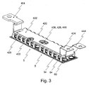
- FIG. 3 shows load connection elements and substrates of a power semiconductor module according to the invention in a three-dimensional representation.
- FIG. 1 shows a section along the line AA (see FIG. 2) through a power semiconductor module (1) according to the invention.
- This has a housing (3) with a frame-like housing part.
- the frame-like housing part encloses the at least one substrate (5).
- This in turn has an insulating body (52), preferably an insulating ceramic, such as aluminum oxide or aluminum nitrite.
- the substrate (5) On the, the interior of the power semiconductor module (1) facing, the first main surface, the substrate (5) has a structured in itself Metallkaschtechnik.
- the individual sections of this metal lamination which is preferably configured as a copper lamination, form the printed conductors (54) of the power semiconductor module (1).
- the second main surface of the substrate (5) according to the prior art, a non-structured Kupferkaschtechnik (56).
- controllable and / or uncontrolled power semiconductor devices such as IGBTs (insulated gate bipolar transistor) arranged in each case with antiparallel freewheeling diodes, or MOS-FETs. These are circuitally connected to other interconnects (54), for example by means of wire bonds (62) connected.
- the load connection elements (40, 42, 44) with the various necessary potentials serve for the external connection of the power electronic circuit inside the power semiconductor module (1).
- the load connection elements (40, 42, 44) are formed as metal moldings, each having a band-like portion (402, 422, 442) parallel to the substrate surface.
- the strip-like sections (402, 422, 442) form a stack, the strip-like sections of the individual load connection elements (40, 42, 44) being separated from one another exclusively by a necessary insulation (46), for example in the form of a plastic film. Necessary auxiliary connection elements are not shown for reasons of clarity in this sectional drawing.
- the power semiconductor module (1) according to the invention has an intermediate layer formed as molded insulating body (30) between the stack of strip-like sections (402, 422, 442) of the load connection elements (40, 42, 44) and the substrate (5).
- This Isolierstoffform Sciences (30) is arranged in this embodiment in the frame-like housing (3) by means of a snap-locking connection (90).
- the Isolierstoffformmaschine (30) in turn has recesses (32) for carrying out the contact feet (400, 420, 440) of the load connection elements (40, 42, 44). It is particularly preferred if these recesses (32) are designed as guides for these contact feet (400, 42, 44), whereby the positioning of the load connection elements (40, 42, 44) relative to the substrate (5) or its conductor tracks (54 ) is again improved over an arrangement with simple recesses.
- the recesses (32) for carrying out the contact feet as wells (34) are formed, wherein these wells (34) come close to close to the surface of the substrate (5).
- these shafts (34) extend into the insulating material layer by way of example into a silicone gel, the silicone gel being applied to the substrate (5) by means of a modern coating method. As a result, a particularly effective internal insulation of the power semiconductor module (1) is formed.
- the pressure device (70) for the thermal connection of the power semiconductor module (1) with a cooling component (2) and at the same time for electrically contacting the load connection elements (40, 42, 44) with the conductor tracks (54) of the substrate (5) is formed by a pressure element ( 72) for pressure build-up and, not shown, an elastic cushion element for pressure storage.
- the pressure is introduced via the cushion member onto the stack of the belt-like portions (402, 422, 442) of the load connection elements (40, 42, 44) and thus exerts pressure on the contact feet (400, 420, 440). As a result, they are electrically connected to conductor tracks (54) of the substrate (5).
- Such pressure contacts (70) have proven to be particularly reliable over the life of power semiconductor modules (1). Also advantageous for the pressure contact is the formation of the recesses (32) of the Isolierstoffform stressess (30) as guides or shafts (34), as a result, the positioning of the contact feet (400, 420, 440) is particularly accurate.
- the pressure element (72) can be designed as a plastic molded body with a suitable metal core embodied as a bimetal, for example, wherein in this case it is also possible to dispense with a cushion element storing the pressure. It is further preferred if the pressure element (72) simultaneously serves as a cover of the power semiconductor module (1).
- Fig. 2 shows a three-dimensional exploded view of a portion of the power semiconductor module (1) according to the invention. Shown here is a plastic housing (3) with means (300) for attachment to a cooling component.
- the housing (3) has an insulating molded body (30) formed integrally therewith, which forms an intermediate layer between the substrate (5) arranged below this intermediate layer and the strip-like sections (402, 422, 442) of the load connection elements (402, 422, 442) arranged above this intermediate layer. 40, 42, 44).
- the housing (3) fastening means (302) for a pressure element (72) not shown, as well as dome-like bushings (38) for auxiliary connection elements (80). It is particularly preferred in such pressure-contacted power semiconductor modules (1) to form the auxiliary connection elements as contact springs (80), preferably coil springs.
- the load connection elements (40, 42, 44) of the various load potentials are each in the form of metal moldings with contact means (404, 424, 444) for external connection, at least one band-like section (402, 422, 442) extending parallel to the substrate surface, and with a plurality of formed out of this section outfeed feet (400, 420, 440).
- the respective load connection elements (40, 42, 44) are as far as necessary by means of an insulating plastic film (46) spaced from each other and electrically isolated from each other.
- the AC connection element (40) furthermore has a current sensor (410) arranged adjacent to the contact device (404).
- the contact feet (400, 420, 440) of the load connection elements (40, 42, 44) extend through the formed as guides recesses (32) of the Isolierstoffform stressess (30) to the associated contact surfaces of the conductor tracks (54) of the substrate (5) and Power semiconductor devices (60).
- the strip-like sections (402, 422, 442) of the load connection elements (40, 42, 44) and their associated insulating plastic films (46) in turn have in those areas recesses (406, 426, 446, 466), in which the housing (3 ) Dome (38) for the auxiliary connection elements (80).
- the associated, not shown, pressure device (70) in turn also has corresponding with the recess of the load connection elements aligned recess for the implementation of the auxiliary connection elements.
- FIG. 3 shows load connection elements (40, 42, 44) of a power semiconductor module (1) according to the invention and their position relative to two substrates (5) in a three-dimensional view without depiction of the housing and the printing device.
- the illustrated circuit of the power semiconductor module is a half-bridge circuit having a plurality of the respective first and second switches forming parallel-connected bipolar transistors (60). Also, the circuit has the necessary free-wheeling diodes (64). The first and second switches of the half-bridge circuit are each distributed in half to two identical substrates.
- a plurality of contact feet (400, 420, 440) of the same polarity in this case contact the associated conductor tracks (54) of the respective polarity on both substrates (5).
- the permanently contact-safe electrical connection is formed by means of the printing device described above.
- recesses (406, 426, 446) of the stack of load connection elements (40, 42, 44) which are provided for the arrangement of the auxiliary connection elements (80) according to FIG. 2.
Landscapes
- Cooling Or The Like Of Semiconductors Or Solid State Devices (AREA)
- Power Conversion In General (AREA)
- Rectifiers (AREA)
Applications Claiming Priority (1)
| Application Number | Priority Date | Filing Date | Title |
|---|---|---|---|
| DE102006006425A DE102006006425B4 (de) | 2006-02-13 | 2006-02-13 | Leistungshalbleitermodul in Druckkontaktausführung |
Publications (3)
| Publication Number | Publication Date |
|---|---|
| EP1843393A2 true EP1843393A2 (fr) | 2007-10-10 |
| EP1843393A3 EP1843393A3 (fr) | 2008-04-30 |
| EP1843393B1 EP1843393B1 (fr) | 2013-03-13 |
Family
ID=38162580
Family Applications (1)
| Application Number | Title | Priority Date | Filing Date |
|---|---|---|---|
| EP07002033A Active EP1843393B1 (fr) | 2006-02-13 | 2007-01-31 | Module de puissance semi-conducteur de type à contact par pression |
Country Status (8)
| Country | Link |
|---|---|
| US (1) | US7589418B2 (fr) |
| EP (1) | EP1843393B1 (fr) |
| JP (1) | JP5114064B2 (fr) |
| KR (1) | KR101204630B1 (fr) |
| CN (1) | CN101064299B (fr) |
| DE (1) | DE102006006425B4 (fr) |
| DK (1) | DK1843393T3 (fr) |
| ES (1) | ES2403072T3 (fr) |
Cited By (2)
| Publication number | Priority date | Publication date | Assignee | Title |
|---|---|---|---|---|
| US7944033B2 (en) | 2007-10-18 | 2011-05-17 | Infineon Technologies Ag | Power semiconductor module |
| DE102014217266A1 (de) * | 2013-10-31 | 2015-04-30 | Mitsubishi Electric Corporation | Halbleitervorrichtung |
Families Citing this family (33)
| Publication number | Priority date | Publication date | Assignee | Title |
|---|---|---|---|---|
| DE102006006423B4 (de) * | 2006-02-13 | 2009-06-10 | Semikron Elektronik Gmbh & Co. Kg | Leistungshalbleitermodul und zugehöriges Herstellungsverfahren |
| DE102006006424B4 (de) * | 2006-02-13 | 2011-11-17 | Semikron Elektronik Gmbh & Co. Kg | Anordnung mit mindestens einem Leistungshalbleitermodul und einem Kühlbauteil und zugehöriges Herstellungsverfahren |
| DE102006052620B4 (de) * | 2006-11-08 | 2009-07-09 | Semikron Elektronik Gmbh & Co. Kg | Schaltungsanordnung mit einem Leistungsmodul, das mit einer Leiterplatte kombiniert ist. |
| DE102006057248B4 (de) | 2006-12-05 | 2009-07-16 | Semikron Elektronik Gmbh & Co. Kg | Halbleitermodul |
| DE102007026768A1 (de) * | 2007-06-09 | 2008-12-11 | Semikron Elektronik Gmbh & Co. Kg | Druckkontaktiertes dreiphasiges Stromrichtermodul |
| US9373563B2 (en) * | 2007-07-20 | 2016-06-21 | Infineon Technologies Ag | Semiconductor assembly having a housing |
| EP2071626A1 (fr) * | 2007-12-11 | 2009-06-17 | ABB Research Ltd. | Module semi-conducteur et dispositif de connexion |
| DE102008034068B4 (de) * | 2008-07-22 | 2019-07-18 | Semikron Elektronik Gmbh & Co. Kg | Leistungshalbleitermodul |
| DE102009005915B4 (de) | 2009-01-23 | 2013-07-11 | Semikron Elektronik Gmbh & Co. Kg | Leistungshalbleitermodul in Druckkontaktausführung |
| DE102009017621B3 (de) * | 2009-04-16 | 2010-08-19 | Semikron Elektronik Gmbh & Co. Kg | Vorrichtung zur Verringerung der Störabstrahlung in einem leistungselektronischen System |
| DE102009035819A1 (de) | 2009-08-01 | 2011-02-03 | Semikron Elektronik Gmbh & Co. Kg | Leistungshalbleitermodul mit stromsymmetrischem Lastanschlusselement |
| DE102009050178B3 (de) | 2009-10-21 | 2011-05-26 | Semikron Elektronik Gmbh & Co. Kg | Leistungshalbleitermodul mit einem eine dreidimensionale Oberflächenkontur aufweisenden Substrat sowie Herstellungsverfahren hierzu |
| DE102009046403B4 (de) | 2009-11-04 | 2015-05-28 | Semikron Elektronik Gmbh & Co. Kg | Leistungshalbleitermodul in Druckkontakttechnik |
| DE102009057145B4 (de) * | 2009-12-05 | 2013-12-19 | Semikron Elektronik Gmbh & Co. Kg | Druckkontaktiertes Leistungshalbleitermodul mit teilweise bandartigen Lastanschlusselementen |
| DE102010000694B4 (de) | 2009-12-18 | 2013-12-12 | Semikron Elektronik Gmbh & Co. Kg | Leistungshalbleitermodul mit Druckkontaktfedern |
| JP5702988B2 (ja) | 2010-01-29 | 2015-04-15 | 株式会社 日立パワーデバイス | 半導体パワーモジュール及びそれが搭載される電力変換装置並びに半導体パワーモジュール搭載用水路形成体の製造方法 |
| DE102010035980B4 (de) * | 2010-09-01 | 2014-03-20 | Semikron Elektronik Gmbh & Co. Kg | Anschlusseinrichtung für ein Leistungshalbleitermodul |
| DE102010041849A1 (de) * | 2010-10-01 | 2012-04-05 | Semikron Elektronik Gmbh & Co. Kg | Leistungshalbleitermodul mit einem Grundmodul und einem Verbindungsmodul |
| DE102010043362A1 (de) | 2010-11-04 | 2012-05-10 | Semikron Elektronik Gmbh & Co. Kg | Leistungshalbleitermodul mit einem Substrat mit einer Mehrzahl gleichartig ausgebildeter Leiterbahngruppen |
| DE102013103116B3 (de) * | 2013-03-27 | 2014-09-18 | Semikron Elektronik Gmbh & Co. Kg | Leistungshalbleitermodul und Verfahren zur Herstellung eines Leistungshalbleitermoduls |
| DE102013104950B3 (de) | 2013-05-14 | 2014-04-30 | Semikron Elektronik Gmbh & Co. Kg | Leistungshalbleitermodul und Anordnung hiermit |
| DE102013104949B3 (de) | 2013-05-14 | 2014-04-24 | Semikron Elektronik Gmbh & Co. Kg | Leistungselektronische Schalteinrichtung und Anordnung hiermit |
| DE102013113764B3 (de) * | 2013-12-10 | 2014-09-25 | Semikron Elektronik Gmbh & Co. Kg | Leistungshalbleitereinrichtung |
| DE102014115565B3 (de) * | 2014-10-27 | 2015-10-22 | Semikron Elektronik Gmbh & Co. Kg | Verfahren zur Herstellung einer Schalteinrichtung mit einer feuchtigkeitsdichten und elektrisch isolierenden Abdeckung und zur Herstellung einer Anordnung hiermit |
| US9431311B1 (en) | 2015-02-19 | 2016-08-30 | Semiconductor Components Industries, Llc | Semiconductor package with elastic coupler and related methods |
| DE102015111204B4 (de) * | 2015-07-10 | 2019-03-07 | Semikron Elektronik Gmbh & Co. Kg | Leistungselektronisches Modul mit Lastanschlusselementen |
| DE102015114188B4 (de) * | 2015-08-26 | 2019-03-07 | Semikron Elektronik Gmbh & Co. Kg | Leistungselektronisches Submodul mit einem zweiteiligen Gehäuse |
| EP3413349A4 (fr) * | 2016-02-03 | 2019-09-11 | Shindengen Electric Manufacturing Co. Ltd. | Dispositif à semi-conducteurs, et procédé de fabrication de celui-ci |
| DE102016105779B3 (de) * | 2016-03-30 | 2017-04-06 | Semikron Elektronik Gmbh & Co. Kg | Drei-Level-Stromrichteranordnung und Verbindungsanordnung hierfür |
| JP6825306B2 (ja) * | 2016-11-02 | 2021-02-03 | 富士電機株式会社 | 半導体装置 |
| CN108010904B (zh) * | 2016-11-02 | 2020-04-24 | 株洲中车时代电气股份有限公司 | 一种功率半导体模块 |
| JP6421859B2 (ja) * | 2017-10-10 | 2018-11-14 | 三菱電機株式会社 | 半導体装置 |
| DE102019111145A1 (de) | 2019-04-30 | 2020-11-05 | Semikron Elektronik Gmbh & Co. Kg | Leistungshalbleitermodul und Verfahren zur Anordnung dieses Leistungshalbleitermoduls auf einem Motor |
Family Cites Families (19)
| Publication number | Priority date | Publication date | Assignee | Title |
|---|---|---|---|---|
| DE3486256T2 (de) * | 1983-09-29 | 1994-05-11 | Toshiba Kawasaki Kk | Halbleiteranordnung in Druckpackung. |
| US5345107A (en) * | 1989-09-25 | 1994-09-06 | Hitachi, Ltd. | Cooling apparatus for electronic device |
| US5243217A (en) * | 1990-11-03 | 1993-09-07 | Fuji Electric Co., Ltd. | Sealed semiconductor device with protruding portion |
| DE4237632A1 (de) * | 1992-11-07 | 1994-05-11 | Export Contor Ausenhandelsgese | Schaltungsanordnung |
| JP2854785B2 (ja) * | 1993-08-30 | 1999-02-03 | 三菱電機株式会社 | 半導体装置およびその製造方法 |
| DE19719703C5 (de) * | 1997-05-09 | 2005-11-17 | eupec Europäische Gesellschaft für Leistungshalbleiter mbH & Co. KG | Leistungshalbleitermodul mit Keramiksubstrat |
| DE19843309A1 (de) * | 1998-09-22 | 2000-03-23 | Asea Brown Boveri | Kurzschlussfestes IGBT Modul |
| DE19903245A1 (de) * | 1999-01-27 | 2000-08-03 | Asea Brown Boveri | Leistungshalbleitermodul |
| DE19903875C2 (de) * | 1999-02-01 | 2001-11-29 | Semikron Elektronik Gmbh | Leistungshalbleiterschaltungsanordnung, insbesondere Stromumrichter, in Druckkontaktierung |
| US6703707B1 (en) * | 1999-11-24 | 2004-03-09 | Denso Corporation | Semiconductor device having radiation structure |
| DE10141114C1 (de) * | 2001-06-08 | 2002-11-21 | Semikron Elektronik Gmbh | Schaltungsanordnung |
| DE10127947C1 (de) * | 2001-08-22 | 2002-10-17 | Semikron Elektronik Gmbh | Schaltungsanordnung |
| EP1367643B1 (fr) * | 2002-05-15 | 2006-04-05 | Tyco Electronics AMP GmbH | Module électronique |
| JP2005012053A (ja) * | 2003-06-20 | 2005-01-13 | Toshiba Corp | 電力用半導体装置 |
| DE102004018476B4 (de) * | 2004-04-16 | 2009-06-18 | Infineon Technologies Ag | Leistungshalbleiteranordnung mit kontaktierender Folie und Anpressvorrichtung |
| DE102004021927B4 (de) * | 2004-05-04 | 2008-07-03 | Semikron Elektronik Gmbh & Co. Kg | Verfahren zur inneren elektrischen Isolation eines Substrats für ein Leistungshalbleitermodul |
| DE102004025609B4 (de) * | 2004-05-25 | 2010-12-09 | Semikron Elektronik Gmbh & Co. Kg | Anordnung in Schraub- Druckkontaktierung mit einem Leistungshalbleitermodul |
| DE102006006424B4 (de) * | 2006-02-13 | 2011-11-17 | Semikron Elektronik Gmbh & Co. Kg | Anordnung mit mindestens einem Leistungshalbleitermodul und einem Kühlbauteil und zugehöriges Herstellungsverfahren |
| DE102006006423B4 (de) * | 2006-02-13 | 2009-06-10 | Semikron Elektronik Gmbh & Co. Kg | Leistungshalbleitermodul und zugehöriges Herstellungsverfahren |
-
2006
- 2006-02-13 DE DE102006006425A patent/DE102006006425B4/de not_active Expired - Lifetime
-
2007
- 2007-01-22 KR KR1020070006581A patent/KR101204630B1/ko active Active
- 2007-01-31 EP EP07002033A patent/EP1843393B1/fr active Active
- 2007-01-31 DK DK07002033.4T patent/DK1843393T3/da active
- 2007-01-31 ES ES07002033T patent/ES2403072T3/es active Active
- 2007-02-09 JP JP2007030494A patent/JP5114064B2/ja active Active
- 2007-02-12 CN CN2007100052646A patent/CN101064299B/zh active Active
- 2007-02-13 US US11/705,728 patent/US7589418B2/en active Active
Cited By (4)
| Publication number | Priority date | Publication date | Assignee | Title |
|---|---|---|---|---|
| US7944033B2 (en) | 2007-10-18 | 2011-05-17 | Infineon Technologies Ag | Power semiconductor module |
| DE102014217266A1 (de) * | 2013-10-31 | 2015-04-30 | Mitsubishi Electric Corporation | Halbleitervorrichtung |
| US9633918B2 (en) | 2013-10-31 | 2017-04-25 | Mitsubishi Electric Corporation | Semiconductor device |
| DE102014217266B4 (de) | 2013-10-31 | 2023-11-16 | Mitsubishi Electric Corporation | Halbleitervorrichtung |
Also Published As
| Publication number | Publication date |
|---|---|
| DK1843393T3 (da) | 2013-06-10 |
| KR101204630B1 (ko) | 2012-11-23 |
| JP5114064B2 (ja) | 2013-01-09 |
| JP2007221126A (ja) | 2007-08-30 |
| CN101064299A (zh) | 2007-10-31 |
| US20070194429A1 (en) | 2007-08-23 |
| EP1843393B1 (fr) | 2013-03-13 |
| US7589418B2 (en) | 2009-09-15 |
| KR20070081744A (ko) | 2007-08-17 |
| DE102006006425B4 (de) | 2009-06-10 |
| EP1843393A3 (fr) | 2008-04-30 |
| DE102006006425A1 (de) | 2007-08-23 |
| ES2403072T3 (es) | 2013-05-13 |
| CN101064299B (zh) | 2010-12-22 |
Similar Documents
| Publication | Publication Date | Title |
|---|---|---|
| EP1843393B1 (fr) | Module de puissance semi-conducteur de type à contact par pression | |
| EP1868243B1 (fr) | Module semi-conducteur de puissance doté d'éléments de connexion isolés électriquement les uns des autres | |
| EP1830404B1 (fr) | Module semi-conducteur de puissance | |
| EP1818982B1 (fr) | Assemblage avec au moins un module semi-conducteur de puissance et un élément de refroidissement et méthode de fabrication associée | |
| EP1840961B1 (fr) | Module semi-conducteur de puissance | |
| DE102009037257B4 (de) | Leistungshalbleitermodul mit Schaltungsträger und Lastanschlusselement sowie Herstellungsverfahren hierzu | |
| DE102007054709B4 (de) | Leistungshalbleitermodul mit einem Substrat und mit einer Druckeinrichtung | |
| DE10340297B4 (de) | Verbindugsanordnung zur Verbindung von aktiven und passiven elektrischen und elektronischen Bauelementen | |
| DE102013216035B3 (de) | Leistungshalbleitermodul und Verfahren zur Herstellung eines Leistungshalbleitermoduls | |
| DE102005055713B4 (de) | Leistungshalbleitermodul mit Anschlusselementen | |
| EP1950807B1 (fr) | Module semi-conducteur de puissance doté d'un corps de pression | |
| DE102006058692A1 (de) | Leistungshalbleitermodul mit Kontaktfedern | |
| EP2003693B1 (fr) | Module de convertisseur de puissance triphasé contacté par pression | |
| DE102009057146A1 (de) | Druckkontaktiertes Leistungshalbleitermodul mit Hybriddruckspeicher | |
| DE102008014113B4 (de) | Leistungshalbleitermodul in Druckkontaktausführung | |
| DE102023207743A1 (de) | Leistungsmodul und Verfahren zu dessen Herstellung | |
| DE102024200743A1 (de) | Halbleiterschaltung | |
| DE102012215651A1 (de) | Verbindungselement zur elektrisch leitenden Verbindung einer ersten Leistungselektronikeinrichtung mit einer zweiten Leistungselektronikeinrichtung | |
| DE102015213085A1 (de) | Leistungsmodul sowie Verfahren zum Herstellen eines Leistungsmoduls |
Legal Events
| Date | Code | Title | Description |
|---|---|---|---|
| PUAI | Public reference made under article 153(3) epc to a published international application that has entered the european phase |
Free format text: ORIGINAL CODE: 0009012 |
|
| AK | Designated contracting states |
Kind code of ref document: A2 Designated state(s): AT BE BG CH CY CZ DE DK EE ES FI FR GB GR HU IE IS IT LI LT LU LV MC NL PL PT RO SE SI SK TR |
|
| AX | Request for extension of the european patent |
Extension state: AL BA HR MK YU |
|
| PUAL | Search report despatched |
Free format text: ORIGINAL CODE: 0009013 |
|
| AK | Designated contracting states |
Kind code of ref document: A3 Designated state(s): AT BE BG CH CY CZ DE DK EE ES FI FR GB GR HU IE IS IT LI LT LU LV MC NL PL PT RO SE SI SK TR |
|
| AX | Request for extension of the european patent |
Extension state: AL BA HR MK RS |
|
| 17P | Request for examination filed |
Effective date: 20080410 |
|
| 17Q | First examination report despatched |
Effective date: 20080623 |
|
| AKX | Designation fees paid |
Designated state(s): AT BE BG CH CY CZ DE DK EE ES FI FR GB GR HU IE IS IT LI LT LU LV MC NL PL PT RO SE SI SK TR |
|
| GRAP | Despatch of communication of intention to grant a patent |
Free format text: ORIGINAL CODE: EPIDOSNIGR1 |
|
| GRAS | Grant fee paid |
Free format text: ORIGINAL CODE: EPIDOSNIGR3 |
|
| GRAA | (expected) grant |
Free format text: ORIGINAL CODE: 0009210 |
|
| AK | Designated contracting states |
Kind code of ref document: B1 Designated state(s): AT BE BG CH CY CZ DE DK EE ES FI FR GB GR HU IE IS IT LI LT LU LV MC NL PL PT RO SE SI SK TR |
|
| REG | Reference to a national code |
Ref country code: GB Ref legal event code: FG4D Free format text: NOT ENGLISH |
|
| REG | Reference to a national code |
Ref country code: AT Ref legal event code: REF Ref document number: 601253 Country of ref document: AT Kind code of ref document: T Effective date: 20130315 Ref country code: CH Ref legal event code: EP |
|
| REG | Reference to a national code |
Ref country code: IE Ref legal event code: FG4D Free format text: LANGUAGE OF EP DOCUMENT: GERMAN |
|
| REG | Reference to a national code |
Ref country code: CH Ref legal event code: NV Representative=s name: BRAUNPAT BRAUN EDER AG, CH |
|
| REG | Reference to a national code |
Ref country code: DE Ref legal event code: R096 Ref document number: 502007011432 Country of ref document: DE Effective date: 20130508 |
|
| REG | Reference to a national code |
Ref country code: ES Ref legal event code: FG2A Ref document number: 2403072 Country of ref document: ES Kind code of ref document: T3 Effective date: 20130513 |
|
| REG | Reference to a national code |
Ref country code: DK Ref legal event code: T3 |
|
| REG | Reference to a national code |
Ref country code: SE Ref legal event code: TRGR |
|
| REG | Reference to a national code |
Ref country code: NL Ref legal event code: T3 |
|
| PG25 | Lapsed in a contracting state [announced via postgrant information from national office to epo] |
Ref country code: LT Free format text: LAPSE BECAUSE OF FAILURE TO SUBMIT A TRANSLATION OF THE DESCRIPTION OR TO PAY THE FEE WITHIN THE PRESCRIBED TIME-LIMIT Effective date: 20130313 Ref country code: BG Free format text: LAPSE BECAUSE OF FAILURE TO SUBMIT A TRANSLATION OF THE DESCRIPTION OR TO PAY THE FEE WITHIN THE PRESCRIBED TIME-LIMIT Effective date: 20130613 |
|
| REG | Reference to a national code |
Ref country code: LT Ref legal event code: MG4D |
|
| PG25 | Lapsed in a contracting state [announced via postgrant information from national office to epo] |
Ref country code: SI Free format text: LAPSE BECAUSE OF FAILURE TO SUBMIT A TRANSLATION OF THE DESCRIPTION OR TO PAY THE FEE WITHIN THE PRESCRIBED TIME-LIMIT Effective date: 20130313 Ref country code: LV Free format text: LAPSE BECAUSE OF FAILURE TO SUBMIT A TRANSLATION OF THE DESCRIPTION OR TO PAY THE FEE WITHIN THE PRESCRIBED TIME-LIMIT Effective date: 20130313 Ref country code: GR Free format text: LAPSE BECAUSE OF FAILURE TO SUBMIT A TRANSLATION OF THE DESCRIPTION OR TO PAY THE FEE WITHIN THE PRESCRIBED TIME-LIMIT Effective date: 20130614 Ref country code: FI Free format text: LAPSE BECAUSE OF FAILURE TO SUBMIT A TRANSLATION OF THE DESCRIPTION OR TO PAY THE FEE WITHIN THE PRESCRIBED TIME-LIMIT Effective date: 20130313 |
|
| PG25 | Lapsed in a contracting state [announced via postgrant information from national office to epo] |
Ref country code: PT Free format text: LAPSE BECAUSE OF FAILURE TO SUBMIT A TRANSLATION OF THE DESCRIPTION OR TO PAY THE FEE WITHIN THE PRESCRIBED TIME-LIMIT Effective date: 20130715 Ref country code: SK Free format text: LAPSE BECAUSE OF FAILURE TO SUBMIT A TRANSLATION OF THE DESCRIPTION OR TO PAY THE FEE WITHIN THE PRESCRIBED TIME-LIMIT Effective date: 20130313 Ref country code: IS Free format text: LAPSE BECAUSE OF FAILURE TO SUBMIT A TRANSLATION OF THE DESCRIPTION OR TO PAY THE FEE WITHIN THE PRESCRIBED TIME-LIMIT Effective date: 20130713 Ref country code: RO Free format text: LAPSE BECAUSE OF FAILURE TO SUBMIT A TRANSLATION OF THE DESCRIPTION OR TO PAY THE FEE WITHIN THE PRESCRIBED TIME-LIMIT Effective date: 20130313 Ref country code: EE Free format text: LAPSE BECAUSE OF FAILURE TO SUBMIT A TRANSLATION OF THE DESCRIPTION OR TO PAY THE FEE WITHIN THE PRESCRIBED TIME-LIMIT Effective date: 20130313 Ref country code: CZ Free format text: LAPSE BECAUSE OF FAILURE TO SUBMIT A TRANSLATION OF THE DESCRIPTION OR TO PAY THE FEE WITHIN THE PRESCRIBED TIME-LIMIT Effective date: 20130313 |
|
| PG25 | Lapsed in a contracting state [announced via postgrant information from national office to epo] |
Ref country code: PL Free format text: LAPSE BECAUSE OF FAILURE TO SUBMIT A TRANSLATION OF THE DESCRIPTION OR TO PAY THE FEE WITHIN THE PRESCRIBED TIME-LIMIT Effective date: 20130313 Ref country code: CY Free format text: LAPSE BECAUSE OF FAILURE TO SUBMIT A TRANSLATION OF THE DESCRIPTION OR TO PAY THE FEE WITHIN THE PRESCRIBED TIME-LIMIT Effective date: 20130313 |
|
| PLBE | No opposition filed within time limit |
Free format text: ORIGINAL CODE: 0009261 |
|
| STAA | Information on the status of an ep patent application or granted ep patent |
Free format text: STATUS: NO OPPOSITION FILED WITHIN TIME LIMIT |
|
| 26N | No opposition filed |
Effective date: 20131216 |
|
| REG | Reference to a national code |
Ref country code: DE Ref legal event code: R097 Ref document number: 502007011432 Country of ref document: DE Effective date: 20131216 |
|
| BERE | Be: lapsed |
Owner name: SEMIKRON ELEKTRONIK G.M.B.H. & CO. KG Effective date: 20140131 |
|
| PG25 | Lapsed in a contracting state [announced via postgrant information from national office to epo] |
Ref country code: LU Free format text: LAPSE BECAUSE OF FAILURE TO SUBMIT A TRANSLATION OF THE DESCRIPTION OR TO PAY THE FEE WITHIN THE PRESCRIBED TIME-LIMIT Effective date: 20140131 Ref country code: MC Free format text: LAPSE BECAUSE OF FAILURE TO SUBMIT A TRANSLATION OF THE DESCRIPTION OR TO PAY THE FEE WITHIN THE PRESCRIBED TIME-LIMIT Effective date: 20130313 |
|
| REG | Reference to a national code |
Ref country code: IE Ref legal event code: MM4A |
|
| PG25 | Lapsed in a contracting state [announced via postgrant information from national office to epo] |
Ref country code: IE Free format text: LAPSE BECAUSE OF NON-PAYMENT OF DUE FEES Effective date: 20140131 Ref country code: BE Free format text: LAPSE BECAUSE OF NON-PAYMENT OF DUE FEES Effective date: 20140131 |
|
| REG | Reference to a national code |
Ref country code: AT Ref legal event code: MM01 Ref document number: 601253 Country of ref document: AT Kind code of ref document: T Effective date: 20140131 |
|
| PG25 | Lapsed in a contracting state [announced via postgrant information from national office to epo] |
Ref country code: AT Free format text: LAPSE BECAUSE OF NON-PAYMENT OF DUE FEES Effective date: 20140131 |
|
| REG | Reference to a national code |
Ref country code: FR Ref legal event code: PLFP Year of fee payment: 10 |
|
| PG25 | Lapsed in a contracting state [announced via postgrant information from national office to epo] |
Ref country code: HU Free format text: LAPSE BECAUSE OF FAILURE TO SUBMIT A TRANSLATION OF THE DESCRIPTION OR TO PAY THE FEE WITHIN THE PRESCRIBED TIME-LIMIT; INVALID AB INITIO Effective date: 20070131 Ref country code: TR Free format text: LAPSE BECAUSE OF FAILURE TO SUBMIT A TRANSLATION OF THE DESCRIPTION OR TO PAY THE FEE WITHIN THE PRESCRIBED TIME-LIMIT Effective date: 20130313 |
|
| REG | Reference to a national code |
Ref country code: FR Ref legal event code: PLFP Year of fee payment: 11 |
|
| PGFP | Annual fee paid to national office [announced via postgrant information from national office to epo] |
Ref country code: NL Payment date: 20170124 Year of fee payment: 11 |
|
| PGFP | Annual fee paid to national office [announced via postgrant information from national office to epo] |
Ref country code: SE Payment date: 20170125 Year of fee payment: 11 |
|
| PGFP | Annual fee paid to national office [announced via postgrant information from national office to epo] |
Ref country code: DK Payment date: 20170125 Year of fee payment: 11 |
|
| REG | Reference to a national code |
Ref country code: FR Ref legal event code: PLFP Year of fee payment: 12 |
|
| REG | Reference to a national code |
Ref country code: CH Ref legal event code: PCAR Free format text: NEW ADDRESS: HOLEESTRASSE 87, 4054 BASEL (CH) |
|
| REG | Reference to a national code |
Ref country code: DK Ref legal event code: EBP Effective date: 20180131 |
|
| REG | Reference to a national code |
Ref country code: NL Ref legal event code: MM Effective date: 20180201 |
|
| REG | Reference to a national code |
Ref country code: SE Ref legal event code: EUG |
|
| PG25 | Lapsed in a contracting state [announced via postgrant information from national office to epo] |
Ref country code: SE Free format text: LAPSE BECAUSE OF NON-PAYMENT OF DUE FEES Effective date: 20180201 |
|
| PG25 | Lapsed in a contracting state [announced via postgrant information from national office to epo] |
Ref country code: NL Free format text: LAPSE BECAUSE OF NON-PAYMENT OF DUE FEES Effective date: 20180201 |
|
| PG25 | Lapsed in a contracting state [announced via postgrant information from national office to epo] |
Ref country code: DK Free format text: LAPSE BECAUSE OF NON-PAYMENT OF DUE FEES Effective date: 20180131 |
|
| REG | Reference to a national code |
Ref country code: DE Ref legal event code: R081 Ref document number: 502007011432 Country of ref document: DE Owner name: SEMIKRON DANFOSS ELEKTRONIK GMBH & CO. KG, DE Free format text: FORMER OWNER: SEMIKRON ELEKTRONIK GMBH & CO. KG, 90431 NUERNBERG, DE |
|
| REG | Reference to a national code |
Ref country code: DE Ref legal event code: R079 Ref document number: 502007011432 Country of ref document: DE Free format text: PREVIOUS MAIN CLASS: H01L0023480000 Ipc: H10W0072000000 |
|
| PGFP | Annual fee paid to national office [announced via postgrant information from national office to epo] |
Ref country code: GB Payment date: 20251211 Year of fee payment: 20 |
|
| PGFP | Annual fee paid to national office [announced via postgrant information from national office to epo] |
Ref country code: FR Payment date: 20251208 Year of fee payment: 20 |
|
| REG | Reference to a national code |
Ref country code: CH Ref legal event code: U11 Free format text: ST27 STATUS EVENT CODE: U-0-0-U10-U11 (AS PROVIDED BY THE NATIONAL OFFICE) Effective date: 20260201 |
|
| PGFP | Annual fee paid to national office [announced via postgrant information from national office to epo] |
Ref country code: ES Payment date: 20260209 Year of fee payment: 20 |
|
| PGFP | Annual fee paid to national office [announced via postgrant information from national office to epo] |
Ref country code: DE Payment date: 20251210 Year of fee payment: 20 |
|
| PGFP | Annual fee paid to national office [announced via postgrant information from national office to epo] |
Ref country code: IT Payment date: 20251219 Year of fee payment: 20 |
|
| PGFP | Annual fee paid to national office [announced via postgrant information from national office to epo] |
Ref country code: CH Payment date: 20260201 Year of fee payment: 20 |