EP1845560A1 - Lichtemittierende Vorrichtung und Verfahren zu ihrer Herstellung - Google Patents
Lichtemittierende Vorrichtung und Verfahren zu ihrer Herstellung Download PDFInfo
- Publication number
- EP1845560A1 EP1845560A1 EP06027013A EP06027013A EP1845560A1 EP 1845560 A1 EP1845560 A1 EP 1845560A1 EP 06027013 A EP06027013 A EP 06027013A EP 06027013 A EP06027013 A EP 06027013A EP 1845560 A1 EP1845560 A1 EP 1845560A1
- Authority
- EP
- European Patent Office
- Prior art keywords
- layer
- contact part
- electrode
- light emitting
- contact
- Prior art date
- Legal status (The legal status is an assumption and is not a legal conclusion. Google has not performed a legal analysis and makes no representation as to the accuracy of the status listed.)
- Withdrawn
Links
Images


Classifications
-
- H—ELECTRICITY
- H10—SEMICONDUCTOR DEVICES; ELECTRIC SOLID-STATE DEVICES NOT OTHERWISE PROVIDED FOR
- H10K—ORGANIC ELECTRIC SOLID-STATE DEVICES
- H10K59/00—Integrated devices, or assemblies of multiple devices, comprising at least one organic light-emitting element covered by group H10K50/00
- H10K59/10—OLED displays
- H10K59/17—Passive-matrix OLED displays
- H10K59/179—Interconnections, e.g. wiring lines or terminals
-
- H—ELECTRICITY
- H05—ELECTRIC TECHNIQUES NOT OTHERWISE PROVIDED FOR
- H05B—ELECTRIC HEATING; ELECTRIC LIGHT SOURCES NOT OTHERWISE PROVIDED FOR; CIRCUIT ARRANGEMENTS FOR ELECTRIC LIGHT SOURCES, IN GENERAL
- H05B33/00—Electroluminescent light sources
- H05B33/12—Light sources with substantially two-dimensional [2D] radiating surfaces
- H05B33/22—Light sources with substantially two-dimensional [2D] radiating surfaces characterised by the chemical or physical composition or the arrangement of auxiliary dielectric or reflective layers
-
- H—ELECTRICITY
- H05—ELECTRIC TECHNIQUES NOT OTHERWISE PROVIDED FOR
- H05B—ELECTRIC HEATING; ELECTRIC LIGHT SOURCES NOT OTHERWISE PROVIDED FOR; CIRCUIT ARRANGEMENTS FOR ELECTRIC LIGHT SOURCES, IN GENERAL
- H05B33/00—Electroluminescent light sources
- H05B33/12—Light sources with substantially two-dimensional [2D] radiating surfaces
- H05B33/26—Light sources with substantially two-dimensional [2D] radiating surfaces characterised by the composition or arrangement of the conductive material used as an electrode
Definitions
- the present invention relates to a light emitting device and a method for manufacturing the same.
- light emitting device has an advantage in that it has high response speed and low power consumption.
- the light emitting device can also be manufactured thin in size and light in weight because of not requiring backlight unit.
- organic light emitting device has an organic light emitting layer between an anode and a cathode. Holes from the anode and electrons from the cathode are combined within the organic light emitting layer to create hole-electron pairs, i.e. , excitons. The organic light emitting device emits lights by energy generated while the excitons return to ground state.
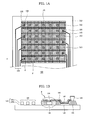
- FIG. 1A is a plan view of a prior art light emitting device
- FIG. 1B is a cross sectional view taken along line A-A' of FIG. 1A.
- the conventional light emitting device 100 comprises a substrate 110, and anodes 120 and wires 125 formed on the substrate 110, each wire 125 comprising a contact part 126 at an end of the wire 125.
- Wires 125 may comprise a conductive layer 125A and a metal layer 125B disposed on the conductive layer 125A.
- An insulating layer 130 is formed on the substrate 110 comprising the anodes 120 and wires 125 having contact parts 126.
- the insulating layer 130 comprises openings 135, each of which exposes a portion of each anode 120, and contact holes 136, each of which exposes a portion of each contact part 126.
- Emission layers 150 are disposed within the openings 135 of the insulating layer 130, and barrier ribs 140 are formed on the insulating layer 130 in the shape of reverse taper.
- Cathodes 160 are disposed on the substrate 110 comprising the barrier ribs 140. The cathodes 160 are patterned by the barrier ribs 140 and connected electrically to the contact parts 126 exposed by the contact holes 136 and the emission layers 150 formed within the openings 135.
- the contact hole 136 is formed to expose a portion of an upper surface of the contact part 126 . Therefore, the contacting area of the contact part 126 and cathode 160 becomes narrow.
- a peeling phenomenon of the insulating layer 130 can occur at the regions contact part 126 other than the regions exposed by the contact holes 136.
- interfacial resistance between the contact part 126 and cathode 160 can be increased because the contacting area between the contact part 126 and cathode 160 are very narrow.
- the present invention provides an organic light emitting device comprising a first electrode and a wire comprising a contact part formed on a substrate, an insulating layer formed on the first electrode and a portion of the wire, the insulating layer comprising an opening which exposes a portion of the first electrode and a contact hole which exposes an entire upper surface of the contact part, an emission layer formed in the opening, a second electrode formed on the emission layer and the upper surface of the contact part though the contact hole.
- the present invention provides a method of fabricating a light emitting device comprising, forming a first electrode and a wire comprising a contact part on a substrate, forming an insulating layer on the first electrode and a portion of the wire, the insulating layer comprising an opening which exposes a portion of the first electrode and a contact hole which exposes an entire upper surface of the contact part, forming an emission layer in the opening, forming a second electrode on the emission layer and the upper surface of the contact part though the contact hole.
- FIG. 1A is a plan view of illustrating a prior art light emitting device.
- FIG. 1B is a cross sectional view taken along line A-A' of FIG. 1A.
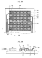
- FIG. 2A is a plan view of a light emitting device according to an embodiment of the present invention.
- FIG. 2B is a cross sectional view taken along line B-B' of FIG. 2A.
- FIGS. 3A to 3H are plan views and cross sectional views for illustrating each process of a method for manufacturing a light emitting device according to an embodiment of the present invention.
- FIGS. 4 to 6 are cross sectional views of a contact region according to other embodiments of the present invention.
- FIG. 2A is a plan view of a light emitting device according to an embodiment of the present invention.
- FIG. 2B is a cross sectional view taken along line B-B' of FIG. 2A.
- the light emitting device 200 comprises a substrate 210, first electrodes 220 and wires 225 each having a contact part 226 at an end of the wire 225, wherein the first electrodes 220 and the wires 225 are disposed on the substrate 210.
- the first electrodes 220 may be anodes and comprise conductive films having high work functions.
- each wire 225 and contact part 226 comprise at least one conductive layer 225A and can be formed as a multiple-structure which comprises multiple metal layers 225B disposed on the conductive layer.
- the conductive layer 225A may comprise Indium Tin Oxide(ITO), Indium Zinc Oxide (IZO) or Indium Tin Zinc Oxide (ITZO), and the metal layer 225B may comprise Molibden(Mo) or Aluminum(Al) . Furthermore, the metal layer 225B may be formed as a triple-layer structure which consists of a first Mo layer, an A1 layer, and a second Molibden layer.
- the wires 225 are connected to cathodes 260 to be subsequently formed to supply electrical signals. While the wires 225 are arranged alternately in the left and right directions to reduce dead spaces, the wiring patterns are not limited thereto.
- An insulating layer 230 is disposed on the first electrodes 220 and a portion of wires 225.
- the insulating layer 230 comprises openings 235 for exposing a portion of the first electrodes 220, and emission layers 250 are disposed within the openings 235.
- the insulating layer 230 further comprises contact holes 236 for exposing entire upper surfaces of the contact parts 226.
- the contact holes 236 can also be formed to expose both upper surfaces and side surfaces of the contact parts 226.
- Barrier ribs 240 are formed on the insulating layer 230 in the shape of reverse taper, and second electrodes 260 are disposed on the substrate 220 comprising the barrier ribs 240.
- the second electrodes 260 may be cathodes which have low work functions and can provide the emission layers 250 with electrons.
- the second electrodes 260 are patterned by the barrier ribs and formed on the emission layers 250 and contact holes 226 exposed by the contact holes 236.
- the second electrode 260 can contact with upper and side surfaces of the contact part 226 through the contact hole 236. Accordingly, as the contacting area between the second electrode 260 and contact part 226 increases, the interfacial resistance therebetween can be greatly lessened. Moreover, because the insulating layer 230 formed on the contact parts 226 are completely eliminated, the problem such as a peeling phenomenon of the insulating layer 230 which has occurred conventionally can be solved.
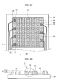
- FIGS. 3B, 3D, 3F, and 3H each are cross sectional views taken along line C-C' of each of FIGS. 3A, 3C, 3E, and 3G.
- conductive layer is formed on a substrate 310 and then first electrodes 320 and wires 325 are formed by patterning the conductive layer.
- the first electrodes 320 are patterned in the shape of stripe and the wires 325 are spaced from the first electrodes 320 and each wire 325 has contact 326 at an end of the wire 325.
- the conductive layer may comprise Indium Tin Oxide (ITO), Indium Zinc Oxide (IZO) or Indium Tin Zinc Oxide (ITZO) .
- the wires 325 comprising the contact parts 326 can be formed as a multiple-layer by depositing a metal layer 325B comprising Molibden or A1 on the conductive layer 325A and then patterning it in order to reduce their resistance.
- the contact parts 326 and wires 325 can be formed as a quadruple-layer structure which consists of ITO/MO/Al/MO.
- an insulating layer 330 is formed on the substrate comprising the first electrodes 320 and wires 325 having the contact parts 326.
- the insulating layer 330 can be formed of silicon oxide(SiO2) or silicon nitride (SiNx) .
- a portion of the insulating layer 330 is etched to form openings 335 for exposing a portion of the first electrodes 320 and contact holes 336 for exposing the contact parts 326.
- the contact holes 336 can also be formed to expose both upper surfaces and side surfaces of the contact parts 326.
- a negative photo-resist is coated on the insulating layer 330 and then exposed to light and developed thereby to form barrier ribs 340.
- the barrier ribs 340 are crossing the first electrodes 320 and can be formed to be spaced from each other.
- emission layers 350 are formed on the first electrodes 320 exposed by the openings 335.
- the emission layers 350 create excitons by recombining electrons and holes to emit lights.
- the emission layers 350 may comprise organic materials.
- the second electrodes 360 are formed on the emission layers 350, upper and side surfaces of the contact parts 326 exposed by the contact holes 336.
- the second electrodes 360 may be cathodes to supply electrons to the emission layers 350, and may be patterned by the barrier ribs 340.
- the contact part 326 has broader contacting area with the second electrode 360 than in the conventional light emitting device because its upper and side surfaces are both exposed by the contact hole 336, and never leaves insulating layer on the contact part 326..
- the light emitting device according to the present invention can reduce the contact resistance between the second electrodes and contact parts and thus reduce its driving voltage. Also, the light emitting device according to the present invention can prevent a peeling phenomenon which has occurred conventionally.
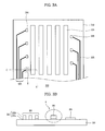
- FIGS. 4 to 6 are cross sectional views of illustrating contact regions (E) of light emitting devices according to other embodiments of the present invention.
- a contact part 426 formed as a multiple-layer structure of ITO/Mo/A1/Mo is disposed on a substrate 410.
- an insulating layer 430 comprising a contact hole 436 for exposing the entire upper surface of the contact part 426.
- a second electrode 460 is disposed, which contacts with the entire upper surface of the contact part 426 through the contact hole 436.
- the interfacial resistance between the second electrode 460 and contact part 426 is reduced because the contacting area therebetween is broad, and therefore the driving voltage of the light emitting device is lowered.
- a contact part 526 formed as a multiple-layer structure of ITO/Mo/Al/Mo is disposed on a substrate 510.
- an insulating layer 530 comprising a contact hole 536 for exposing a portion of the upper and side surfaces of the contact part 526.
- a second electrode 560 is disposed, which contacts with the entire upper surface and a portion of the side surfaces of the contact part 526 through the contact hole 536.
- the interfacial resistance between the second electrode 560 and contact part 526 is reduced because the contacting area therebetween is broad, and therefore the driving voltage of a light emitting device is lowered.
- the second electrode 560 is typically formed of A1. Therefore, in the case that the contact hole 536 is formed to expose the A1 layer of the contact part 526 as shown in FIG. 5, the adherence strength between the second electrode 560 and contact part 526 can be enhanced and the interfacial resistance between the second electrode 560 and contact part 526 can be effectively reduced because the contact part 526 has the same material as the second electrode 560.
- a contact part 626 formed as a multiple-layer structure of ITO/Mo/Al/Mo is disposed on a substrate 610.
- an insulating layer 626 comprising a contact hole 636 for exposing a portion of the upper and side surfaces of the contact part 630.
- a second electrode 660 is disposed, which contacts with a portion of the upper and side surfaces of the contact part 626 through the contact hole 636.
- the interfacial resistance between the second electrode 460 and contact part 426 is reduced because the contacting area therebetween is broad, and therefore the driving voltage of the light emitting device can be lowered.
Landscapes
- Electroluminescent Light Sources (AREA)
- Devices For Indicating Variable Information By Combining Individual Elements (AREA)
Applications Claiming Priority (1)
| Application Number | Priority Date | Filing Date | Title |
|---|---|---|---|
| KR1020060032511A KR100736576B1 (ko) | 2006-04-10 | 2006-04-10 | 전계발광소자와 그 제조방법 |
Publications (1)
| Publication Number | Publication Date |
|---|---|
| EP1845560A1 true EP1845560A1 (de) | 2007-10-17 |
Family
ID=38229253
Family Applications (1)
| Application Number | Title | Priority Date | Filing Date |
|---|---|---|---|
| EP06027013A Withdrawn EP1845560A1 (de) | 2006-04-10 | 2006-12-28 | Lichtemittierende Vorrichtung und Verfahren zu ihrer Herstellung |
Country Status (5)
| Country | Link |
|---|---|
| US (1) | US7786519B2 (de) |
| EP (1) | EP1845560A1 (de) |
| JP (1) | JP2007279680A (de) |
| KR (1) | KR100736576B1 (de) |
| CN (1) | CN101055886A (de) |
Families Citing this family (6)
| Publication number | Priority date | Publication date | Assignee | Title |
|---|---|---|---|---|
| JP5435260B2 (ja) * | 2009-04-03 | 2014-03-05 | ソニー株式会社 | 表示装置およびその製造方法 |
| CN101789493B (zh) * | 2009-12-25 | 2012-11-07 | 昆山维信诺显示技术有限公司 | 一种有机电致发光器件 |
| KR101825053B1 (ko) * | 2011-01-11 | 2018-02-05 | 삼성디스플레이 주식회사 | 유기발광표시장치의 제조방법 |
| KR102823585B1 (ko) * | 2016-12-07 | 2025-06-20 | 삼성디스플레이 주식회사 | 유기 발광 표시 장치 및 그 제조 방법 |
| CN107170788A (zh) * | 2017-06-06 | 2017-09-15 | 武汉华星光电技术有限公司 | 一种显示屏 |
| CN113097255B (zh) * | 2021-03-17 | 2022-10-04 | 深圳市华星光电半导体显示技术有限公司 | 阵列基板及其制作方法 |
Citations (4)
| Publication number | Priority date | Publication date | Assignee | Title |
|---|---|---|---|---|
| WO2002089177A2 (en) * | 2001-04-26 | 2002-11-07 | Samsung Electronics Co., Ltd. | A contact structure of a wiring line and method manufacturing the same, and thin film transistor array substrate including the contact structure and method manufacturing the same |
| US20060001365A1 (en) * | 2004-07-02 | 2006-01-05 | Chae Byung-Hoon | Light emitting display device |
| EP1648033A2 (de) * | 2004-10-14 | 2006-04-19 | LG Electronics Inc. | Organische elektrolumineszente Anzeigevorrichtung und Verfahren zu deren Herstellung |
| EP1715533A2 (de) * | 2005-04-19 | 2006-10-25 | LG Electronics Inc. | Lichtemittierende Vorrichtung und Verfahren zu seiner Herstellung |
Family Cites Families (16)
| Publication number | Priority date | Publication date | Assignee | Title |
|---|---|---|---|---|
| JP2739855B2 (ja) * | 1995-12-14 | 1998-04-15 | 日本電気株式会社 | 半導体装置およびその製造方法 |
| US5990507A (en) * | 1996-07-09 | 1999-11-23 | Kabushiki Kaisha Toshiba | Semiconductor device having ferroelectric capacitor structures |
| JPH11214504A (ja) * | 1998-01-26 | 1999-08-06 | Mitsubishi Electric Corp | 半導体装置およびその製造方法 |
| JP3927323B2 (ja) * | 1998-09-11 | 2007-06-06 | パイオニア株式会社 | 有機elフルカラーディスプレイパネルおよびその製造方法 |
| KR100299537B1 (ko) * | 1999-08-31 | 2001-11-01 | 남상희 | 엑스-선 검출용 박막트랜지스터 기판 제조방법 |
| JP2001102169A (ja) * | 1999-10-01 | 2001-04-13 | Sanyo Electric Co Ltd | El表示装置 |
| JP2001194676A (ja) * | 2000-01-07 | 2001-07-19 | Hitachi Ltd | 液晶表示装置 |
| KR100379566B1 (ko) * | 2000-08-30 | 2003-04-10 | 엘지.필립스 엘시디 주식회사 | 액정표시장치 제조방법 |
| KR100695303B1 (ko) * | 2000-10-31 | 2007-03-14 | 삼성전자주식회사 | 제어 신호부 및 그 제조 방법과 이를 포함하는 액정 표시장치 및 그 제조 방법 |
| KR100408414B1 (ko) * | 2001-06-20 | 2003-12-06 | 삼성전자주식회사 | 반도체 소자 및 그 제조방법 |
| JP5046445B2 (ja) * | 2001-07-31 | 2012-10-10 | 株式会社半導体エネルギー研究所 | 半導体装置の作製方法 |
| JP4271915B2 (ja) * | 2002-04-11 | 2009-06-03 | オプトレックス株式会社 | 有機エレクトロルミネセンス表示素子、有機エレクトロルミネセンス表示装置 |
| KR100813833B1 (ko) | 2002-08-23 | 2008-03-17 | 삼성에스디아이 주식회사 | 전자 발광 소자와 그 제조방법 |
| JP3791618B2 (ja) * | 2003-02-20 | 2006-06-28 | セイコーエプソン株式会社 | 電気光学装置及びその製造方法並びに電子機器 |
| JP2004296665A (ja) * | 2003-03-26 | 2004-10-21 | Seiko Epson Corp | 半導体装置、電気光学装置、および電子機器 |
| KR100560787B1 (ko) * | 2003-11-05 | 2006-03-13 | 삼성에스디아이 주식회사 | 유기전계발광표시장치 |
-
2006
- 2006-04-10 KR KR1020060032511A patent/KR100736576B1/ko not_active Expired - Fee Related
- 2006-12-25 JP JP2006347635A patent/JP2007279680A/ja active Pending
- 2006-12-27 US US11/645,541 patent/US7786519B2/en active Active
- 2006-12-28 EP EP06027013A patent/EP1845560A1/de not_active Withdrawn
- 2006-12-29 CN CNA2006101720908A patent/CN101055886A/zh active Pending
Patent Citations (4)
| Publication number | Priority date | Publication date | Assignee | Title |
|---|---|---|---|---|
| WO2002089177A2 (en) * | 2001-04-26 | 2002-11-07 | Samsung Electronics Co., Ltd. | A contact structure of a wiring line and method manufacturing the same, and thin film transistor array substrate including the contact structure and method manufacturing the same |
| US20060001365A1 (en) * | 2004-07-02 | 2006-01-05 | Chae Byung-Hoon | Light emitting display device |
| EP1648033A2 (de) * | 2004-10-14 | 2006-04-19 | LG Electronics Inc. | Organische elektrolumineszente Anzeigevorrichtung und Verfahren zu deren Herstellung |
| EP1715533A2 (de) * | 2005-04-19 | 2006-10-25 | LG Electronics Inc. | Lichtemittierende Vorrichtung und Verfahren zu seiner Herstellung |
Also Published As
| Publication number | Publication date |
|---|---|
| US20070235767A1 (en) | 2007-10-11 |
| US7786519B2 (en) | 2010-08-31 |
| CN101055886A (zh) | 2007-10-17 |
| KR100736576B1 (ko) | 2007-07-06 |
| JP2007279680A (ja) | 2007-10-25 |
Similar Documents
| Publication | Publication Date | Title |
|---|---|---|
| EP2939291B1 (de) | Organische lichtemittierende anzeigevorrichtung | |
| CN112103326A (zh) | 显示面板及其制造方法、显示装置 | |
| JP2009206041A (ja) | 有機発光装置およびその製造方法 | |
| WO2018049891A1 (zh) | Oled封装基板及其制造方法、oled显示面板 | |
| CN115020621A (zh) | 显示面板、显示面板的制备方法及显示终端 | |
| CN115623879A (zh) | 显示基板、显示面板和显示基板制造方法 | |
| US7786519B2 (en) | Light emitting device and method for manufacturing the same | |
| KR20170078168A (ko) | 유기 발광 표시 장치 및 이의 제조 방법 | |
| JPH11144877A (ja) | 有機発光素子 | |
| EP1608017B1 (de) | Organische elektrolumineszente Anzeigevorrichtung und Herstellungsverfahren | |
| KR102311938B1 (ko) | 유기전계발광 표시장치 및 그 제조 방법 | |
| JP2009187774A (ja) | 有機エレクトロルミネセンス素子 | |
| JP2006128110A (ja) | 有機電界発光表示素子及びその製造方法 | |
| US12588391B2 (en) | OLED display panel and method of fabricating OLED display panel | |
| US12563944B2 (en) | OLED display panel | |
| JP7493080B2 (ja) | 発光装置 | |
| CN109585491A (zh) | 窄边框的有机发光二极管显示器 | |
| JP6341692B2 (ja) | 発光装置 | |
| CN110098344B (zh) | 柔性显示面板 | |
| JP6441306B2 (ja) | 発光装置 | |
| KR101136620B1 (ko) | 유기 발광 다이오드 디스플레이 패널의 양극 배선 공정방법 | |
| KR100946371B1 (ko) | 유기 발광 표시 장치 및 그 제조 방법 | |
| JP4905838B2 (ja) | 有機elパネル | |
| JP2018129313A (ja) | 発光装置 | |
| JPH10106751A (ja) | 有機薄膜エレクトロルミネッセンス表示装置の電極構造 |
Legal Events
| Date | Code | Title | Description |
|---|---|---|---|
| PUAI | Public reference made under article 153(3) epc to a published international application that has entered the european phase |
Free format text: ORIGINAL CODE: 0009012 |
|
| 17P | Request for examination filed |
Effective date: 20061228 |
|
| AK | Designated contracting states |
Kind code of ref document: A1 Designated state(s): AT BE BG CH CY CZ DE DK EE ES FI FR GB GR HU IE IS IT LI LT LU LV MC NL PL PT RO SE SI SK TR |
|
| AX | Request for extension of the european patent |
Extension state: AL BA HR MK YU |
|
| 17Q | First examination report despatched |
Effective date: 20080521 |
|
| AKX | Designation fees paid |
Designated state(s): DE FR GB |
|
| STAA | Information on the status of an ep patent application or granted ep patent |
Free format text: STATUS: THE APPLICATION IS DEEMED TO BE WITHDRAWN |
|
| 18D | Application deemed to be withdrawn |
Effective date: 20120614 |