EP1845561A2 - Dispositif de semi-conducteurs comprenant une diode à hétérojonction et son procédé de fabrication - Google Patents
Dispositif de semi-conducteurs comprenant une diode à hétérojonction et son procédé de fabrication Download PDFInfo
- Publication number
- EP1845561A2 EP1845561A2 EP07007103A EP07007103A EP1845561A2 EP 1845561 A2 EP1845561 A2 EP 1845561A2 EP 07007103 A EP07007103 A EP 07007103A EP 07007103 A EP07007103 A EP 07007103A EP 1845561 A2 EP1845561 A2 EP 1845561A2
- Authority
- EP
- European Patent Office
- Prior art keywords
- region
- semiconductor region
- semiconductor
- semiconductor device
- heterojunction
- Prior art date
- Legal status (The legal status is an assumption and is not a legal conclusion. Google has not performed a legal analysis and makes no representation as to the accuracy of the status listed.)
- Granted
Links
Images


Classifications
-
- H—ELECTRICITY
- H10—SEMICONDUCTOR DEVICES; ELECTRIC SOLID-STATE DEVICES NOT OTHERWISE PROVIDED FOR
- H10D—INORGANIC ELECTRIC SEMICONDUCTOR DEVICES
- H10D84/00—Integrated devices formed in or on semiconductor substrates that comprise only semiconducting layers, e.g. on Si wafers or on GaAs-on-Si wafers
- H10D84/101—Integrated devices comprising main components and built-in components, e.g. IGBT having built-in freewheel diode
- H10D84/141—VDMOS having built-in components
- H10D84/148—VDMOS having built-in components the built-in components being breakdown diodes, e.g. Zener diodes
-
- H—ELECTRICITY
- H10—SEMICONDUCTOR DEVICES; ELECTRIC SOLID-STATE DEVICES NOT OTHERWISE PROVIDED FOR
- H10F—INORGANIC SEMICONDUCTOR DEVICES SENSITIVE TO INFRARED RADIATION, LIGHT, ELECTROMAGNETIC RADIATION OF SHORTER WAVELENGTH OR CORPUSCULAR RADIATION
- H10F30/00—Individual radiation-sensitive semiconductor devices in which radiation controls the flow of current through the devices, e.g. photodetectors
- H10F30/20—Individual radiation-sensitive semiconductor devices in which radiation controls the flow of current through the devices, e.g. photodetectors the devices having potential barriers, e.g. phototransistors
- H10F30/21—Individual radiation-sensitive semiconductor devices in which radiation controls the flow of current through the devices, e.g. photodetectors the devices having potential barriers, e.g. phototransistors the devices being sensitive to infrared, visible or ultraviolet radiation
- H10F30/22—Individual radiation-sensitive semiconductor devices in which radiation controls the flow of current through the devices, e.g. photodetectors the devices having potential barriers, e.g. phototransistors the devices being sensitive to infrared, visible or ultraviolet radiation the devices having only one potential barrier, e.g. photodiodes
- H10F30/222—Individual radiation-sensitive semiconductor devices in which radiation controls the flow of current through the devices, e.g. photodetectors the devices having potential barriers, e.g. phototransistors the devices being sensitive to infrared, visible or ultraviolet radiation the devices having only one potential barrier, e.g. photodiodes the potential barrier being a PN heterojunction
-
- H—ELECTRICITY
- H10—SEMICONDUCTOR DEVICES; ELECTRIC SOLID-STATE DEVICES NOT OTHERWISE PROVIDED FOR
- H10D—INORGANIC ELECTRIC SEMICONDUCTOR DEVICES
- H10D30/00—Field-effect transistors [FET]
- H10D30/60—Insulated-gate field-effect transistors [IGFET]
- H10D30/63—Vertical IGFETs
- H10D30/635—Vertical IGFETs having no inversion channels, e.g. vertical accumulation channel FETs [ACCUFET] or normally-on vertical IGFETs
-
- H—ELECTRICITY
- H10—SEMICONDUCTOR DEVICES; ELECTRIC SOLID-STATE DEVICES NOT OTHERWISE PROVIDED FOR
- H10D—INORGANIC ELECTRIC SEMICONDUCTOR DEVICES
- H10D30/00—Field-effect transistors [FET]
- H10D30/60—Insulated-gate field-effect transistors [IGFET]
- H10D30/64—Double-diffused metal-oxide semiconductor [DMOS] FETs
- H10D30/66—Vertical DMOS [VDMOS] FETs
-
- H—ELECTRICITY
- H10—SEMICONDUCTOR DEVICES; ELECTRIC SOLID-STATE DEVICES NOT OTHERWISE PROVIDED FOR
- H10D—INORGANIC ELECTRIC SEMICONDUCTOR DEVICES
- H10D30/00—Field-effect transistors [FET]
- H10D30/80—FETs having rectifying junction gate electrodes
- H10D30/83—FETs having PN junction gate electrodes
- H10D30/831—Vertical FETs having PN junction gate electrodes
-
- H—ELECTRICITY
- H10—SEMICONDUCTOR DEVICES; ELECTRIC SOLID-STATE DEVICES NOT OTHERWISE PROVIDED FOR
- H10D—INORGANIC ELECTRIC SEMICONDUCTOR DEVICES
- H10D62/00—Semiconductor bodies, or regions thereof, of devices having potential barriers
- H10D62/80—Semiconductor bodies, or regions thereof, of devices having potential barriers characterised by the materials
- H10D62/82—Heterojunctions
- H10D62/822—Heterojunctions comprising only Group IV materials heterojunctions, e.g. Si/Ge heterojunctions
-
- H—ELECTRICITY
- H10—SEMICONDUCTOR DEVICES; ELECTRIC SOLID-STATE DEVICES NOT OTHERWISE PROVIDED FOR
- H10D—INORGANIC ELECTRIC SEMICONDUCTOR DEVICES
- H10D62/00—Semiconductor bodies, or regions thereof, of devices having potential barriers
- H10D62/80—Semiconductor bodies, or regions thereof, of devices having potential barriers characterised by the materials
- H10D62/83—Semiconductor bodies, or regions thereof, of devices having potential barriers characterised by the materials being Group IV materials, e.g. B-doped Si or undoped Ge
- H10D62/832—Semiconductor bodies, or regions thereof, of devices having potential barriers characterised by the materials being Group IV materials, e.g. B-doped Si or undoped Ge being Group IV materials comprising two or more elements, e.g. SiGe
- H10D62/8325—Silicon carbide
-
- H—ELECTRICITY
- H10—SEMICONDUCTOR DEVICES; ELECTRIC SOLID-STATE DEVICES NOT OTHERWISE PROVIDED FOR
- H10D—INORGANIC ELECTRIC SEMICONDUCTOR DEVICES
- H10D8/00—Diodes
-
- H—ELECTRICITY
- H10—SEMICONDUCTOR DEVICES; ELECTRIC SOLID-STATE DEVICES NOT OTHERWISE PROVIDED FOR
- H10D—INORGANIC ELECTRIC SEMICONDUCTOR DEVICES
- H10D8/00—Diodes
- H10D8/01—Manufacture or treatment
- H10D8/051—Manufacture or treatment of Schottky diodes
-
- H—ELECTRICITY
- H10—SEMICONDUCTOR DEVICES; ELECTRIC SOLID-STATE DEVICES NOT OTHERWISE PROVIDED FOR
- H10D—INORGANIC ELECTRIC SEMICONDUCTOR DEVICES
- H10D8/00—Diodes
- H10D8/60—Schottky-barrier diodes
-
- H—ELECTRICITY
- H10—SEMICONDUCTOR DEVICES; ELECTRIC SOLID-STATE DEVICES NOT OTHERWISE PROVIDED FOR
- H10D—INORGANIC ELECTRIC SEMICONDUCTOR DEVICES
- H10D8/00—Diodes
- H10D8/825—Diodes having bulk potential barriers, e.g. Camel diodes, planar doped barrier diodes or graded bandgap diodes
-
- H—ELECTRICITY
- H10—SEMICONDUCTOR DEVICES; ELECTRIC SOLID-STATE DEVICES NOT OTHERWISE PROVIDED FOR
- H10D—INORGANIC ELECTRIC SEMICONDUCTOR DEVICES
- H10D30/00—Field-effect transistors [FET]
- H10D30/60—Insulated-gate field-effect transistors [IGFET]
- H10D30/64—Double-diffused metal-oxide semiconductor [DMOS] FETs
- H10D30/66—Vertical DMOS [VDMOS] FETs
- H10D30/665—Vertical DMOS [VDMOS] FETs having edge termination structures
-
- H—ELECTRICITY
- H10—SEMICONDUCTOR DEVICES; ELECTRIC SOLID-STATE DEVICES NOT OTHERWISE PROVIDED FOR
- H10D—INORGANIC ELECTRIC SEMICONDUCTOR DEVICES
- H10D62/00—Semiconductor bodies, or regions thereof, of devices having potential barriers
- H10D62/10—Shapes, relative sizes or dispositions of the regions of the semiconductor bodies; Shapes of the semiconductor bodies
- H10D62/102—Constructional design considerations for preventing surface leakage or controlling electric field concentration
- H10D62/103—Constructional design considerations for preventing surface leakage or controlling electric field concentration for increasing or controlling the breakdown voltage of reverse-biased devices
- H10D62/105—Constructional design considerations for preventing surface leakage or controlling electric field concentration for increasing or controlling the breakdown voltage of reverse-biased devices by having particular doping profiles, shapes or arrangements of PN junctions; by having supplementary regions, e.g. junction termination extension [JTE]
- H10D62/106—Constructional design considerations for preventing surface leakage or controlling electric field concentration for increasing or controlling the breakdown voltage of reverse-biased devices by having particular doping profiles, shapes or arrangements of PN junctions; by having supplementary regions, e.g. junction termination extension [JTE] having supplementary regions doped oppositely to or in rectifying contact with regions of the semiconductor bodies, e.g. guard rings with PN or Schottky junctions
Definitions
- the present invention relates to a semiconductor device including a high resistance heterojunction diode and a manufacturing method thereof.
- an N-type polycrystalline silicon region is formed in a contactingmanner on one main surface of a semiconductor base substrate formed with an N - -type epitaxial region on an N + -type substrate region, and the epitaxial region and the N-type polycrystalline silicon region form a heterojunction.
- a rear surface electrode is formed on the rear surface of the N + -type substrate region.
- the present invention has been achieved in view of the above problems, and an obj ect thereof is to provide a semiconductor device having a higher avalanche resistance characteristic as compared to a Schottky junction diode, and a manufacturing method thereof.
- the means for solving the conventional problems is a semiconductor device including a heterojunction diode configured by a first semiconductor region and a second semiconductor region having a band gap different from that of the first semiconductor region and forming heterojunction with the first semiconductor region, wherein the heterojunction region is formed such that when a predetermined reverse bias is applied to the heterojunction diode, a breakdown voltage at least in a heterojunction region other than outer peripheral ends of the heterojunction diode is a breakdown voltage of the semiconductor device.
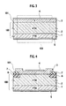
- Fig. 1 is a cross-sectional view showing a configuration of a semiconductor device according to a first embodiment of the present invention.
- the semiconductor device of the first embodiment shown in Fig. 1 configures a heterojunction diode in which a heterojunction between silicon carbide and silicon is employed.
- silicon carbide is employed as a substrate material of a first semiconductor region 100.
- the first semiconductor region 100 is configured by a substrate material in which an N - -type drift region 2 is formed on an N + -type substrate region 1 of which the polytype of silicon carbide is 4H, for example.
- an explanation is given of a case where the impurity density of 10 16 cm -3 and thickness of 10 ⁇ m, for example, is used.
- a substrate comprised solely of the substrate region 1 can be used, irrespective of the magnitude of the resistivity.
- a first hetero semiconductor region 3 comprised of polycrystalline silicon, of which band gap is smaller than that of silicon carbide, is stacked and formed so as to contact a main surface that opposes a junction surface, of the drift region 2, with the substrate region 1.
- a heterojunction diode made of a material, of which band gap of the polycrystalline silicon is different from that of silicon carbide, is formed, and on the junction interface, an energetic barrier exists.
- the impurity density of the first hetero semiconductor region 3 is set such that avalanche breakdown occurs at least in the first hetero semiconductor region 3. For example, an explanation is given of a case where the conductivity type is P-type, the impurity density is 10 17 cm -3 , and the thickness is 0.5 ⁇ m.
- a first electrode 4 is formed so as to contact the first hetero semiconductor region 3, and a second electrode 5 is formed so as to contact the substrate region 1, respectively.
- Fig. 1 shows a case where end portions of the heterojunction portion between the drift region 2 and the first hetero semiconductor region 3 define outermost peripheral ends of the active region.
- electric-field relaxation regions 6 are formed in the end portions.
- the electric-field relaxation regions 6 function to relax an amount of the change.
- the electric-field relaxation region 6 is configured by a material made of 4H-SiC, of which conductivity type is P-type opposite to the drift region 2.
- the electric-field relaxation regions 6 can be inactive regions having a high resistance, and configured by a material having high insulation such as SiO 2 .
- configured is a vertical diode where the first electrode 4 is an anode and the second electrode 5 is a cathode.
- the second electrode 5 (cathode) is aground potential, and apositive electric potential is applied to the first electrode 4 (anode), the heterojunction diode shows a forward characteristic, and shows a conductive characteristic like a Schottky junction diode, similarly to the conventional structure. That is, in the forward characteristic, a forward current passes by a voltage drop determined by a sum of contained electric potentials spread from the heterojunction portion to both sides of the drift region 2 and the first hetero semiconductor region 3. For example, in this first embodiment, the sum of the contained electric potentials spread from the heterojunctionportion to the both sides of the drift region 2 and the first hetero semiconductor region 3 is about 1.2 V. Thus, a forward current passes by the voltage drop corresponding thereto.
- a forward bias is generated.
- a contained electric potential is about 3V, and thus, a current does not pass between the electric-field relaxation regions 6 and the drift region 2.
- the first electrode 4 (anode) is a ground potential, and a positive electric potential is applied to the second electrode 5 (cathode) , the heterojunction diode shows a reverse characteristic, hence showing a cutoff characteristic.
- the conductivity type of the first hetero semiconductor region 3 is P-type.
- the cutoff characteristic operates like a PN junction diode.
- the leakage current characteristic of the Schottky junction diode is determined almost uniquely by a height of a Schottky barrier formed by a difference between an electron affinity of a semiconductor material and a work function of a Schottky metal.
- the heterojunction diode in the conventional structure and in the first embodiment is configured by a junction formed of different semiconductor materials.
- the leakage current characteristic is determined by the height of the energetic barrier occurring mainly betweendifferent semiconductormaterials and a magnitude of a supply source of a majority carrier, which is the origin of the leakage current.
- the height of the energetic barrier is approximately determined by each of the semiconductor materials of the drift region 2 comprised of silicon carbide and the first heterosemiconductorregion3 comprisedof silicon.
- the height of the energetic barrier has a performance similar to that of the Schottky junction diode or the conventional structure.
- the supply source of the majority carrier which serves as the origin of the leakage current, is significantly small as compared to the case of the Schottky junction diode and the conventional structure. That is, this is due to the fact that the first hetero semiconductor region 3 is configured by P-type. Thereby, it becomes difficult for conduction electrons, which serve as the majority carrier for the N-type drift region 2, to be generated in the first hetero semiconductor region 3 , resulting in a configuration where the origin of generation of the conduction electrons is suppressed.
- the impurity density and the thickness of the first hetero semiconductor region 3 are appropriately adjusted so that the entire first hetero semiconductor region 3 do not become depleted when the positive electric potential applied to the second electrode 5 (cathode) is increased. In doing so, the conduction electrons are not directly supplied to the drift region 2 from the first electrode 4 that serves as a conduction-electron supplying source on the anode side.
- the thickness of the remaining region, which remains undepleted, of the first hetero semiconductor region 3 is larger than a diffusion length of electrons in the first hetero semiconductor region 3, it is possible to further cut-off from the supply source of the electrons. Thereby, a leakage current characteristic significantly lower as compared to the Schottky junction diode and the conventional structure is provided in the first embodiment.
- the main region 103 of the active region has a high retention capability in the first place because of retention by a plurality of semiconductor materials rather than retention by a single semiconductor material. Even so, when the impurity density on the semiconductor material side of which band gap is narrow (in this case, this side corresponds to the side of the first hetero semiconductor region 3) is made higher than that of the drift region 2, the main region 103 of the active region can be imparted a higher retention capability. That is, this is made possible because the voltage applied between the cathode/anode canbe allotted such that the voltage of the drift region 2 side, which has a higher voltage retention capability, is higher.
- the avalanche breakdown voltage of the active region is reached. That is, by lowering the impurity density of the first hetero semiconductor region 3 than a predetermined value, the avalanche breakdown can be caused in any place on a surface where the first hetero semiconductor region 3 and the drift region 2 contact at equal timing of or earlier than in the drift region 2 that contacts the electric-field relaxation regions 6 formed in outer peripheral ends of the active region, and thus, a higher avalanche resistance can be demonstrated.
- the reason for that is as follows.
- 4H-SiC configuring the drift region 2 shown in the first embodiment has a high dielectric breakdown field characteristic.
- the dielectric breakdown electric field of 4H-SiC is about 2.8 MV/cm.
- the first hetero semiconductor region 3 is comprised of polycrystalline silicon.
- the magnitude of the dielectric breakdown electric field varies depending on the magnitude of the impurity density introduced in Si.
- the dielectric breakdown electric field is about 0.6 MV/cm.
- the dielectric breakdown electric field is probably about 3 MV/cm.
- the heterojunction interface has the highest electric field in a portion in which formed is a planarized heterojunction where the drift region 2 and the first hetero semiconductor region 3 face.
- a comparison is made by using the data found in the reference document.
- the impurity density of the first hetero semiconductor region 3 of about 10 19 cm -3 is used as a reference, it can be supposed that at least in the planarized portion, the avalanche breakdown occurs on the side of Si (the first hetero semiconductor region 3) when the impurity density falls below the reference, and the avalanche breakdown occurs on the side of 4H-SiC (drift region 2) when the impurity density exceeds the reference. Accordingly, it is understood that at least in the planarized portion, the avalanche breakdown occurs in the entire first hetero semiconductor region 3 in the configuration shown in the first embodiment where the impurity density of the first hetero semiconductor region 3 is 10 17 cm -3 .
- the electric-field relaxation regions 6 formed so as to correspond to endportions of the first hetero semiconductor region 3 relaxanelectric field concentration toward the end portions of the first hetero semiconductor region 3. That is, this is due to the fact that in a portion where the drift region 2 and the electric-field relaxation regions 6 contact, an electric potential distribution occurs between the drift region 2 and the electric-field relaxation regions 6, and almost no electric potential distribution occurs in the end portions of the first hetero semiconductor region 3. Accordingly, in the first hetero semiconductor region 3, the electric potential distribution is spread on the planarized junction surface contacting the drift region 2.
- an electric field concentration is relaxed in a portion that contacts the electric-field relaxation regions 6 as compared to a case where the electric-field relaxation regions 6 are not formed.
- this portion has a high electric field distribution as compared to the planarized portion that contacts the first hetero semiconductor region 3. This allows the voltage applied between the cathode/anode to reach a predetermined value, and as a result, the avalanche breakdown occurs in the first hetero semiconductor region 3 that contacts the drift region 2 or in neighboring areas of the drift region 2 that contacts the electric-field relaxation regions 6.
- the impurity density of the first hetero semiconductor region 3 it becomes possible to control the dielectric breakdown electric field of the first hetero semiconductor region3.
- the impurity density of the first hetero semiconductor region 3 can be adjusted and set such that the avalanche breakdown occurs at equal timing of or earlier than in a portion of the drift region 2, which contacts the electric-field relaxation regions 6 and has the highest electric field.
- Such a characteristic technique permits occurrence of the avalanche breakdown on the entire junction surface of the heterojunction portion that contacts the drift region 2 in also the semiconductor device, including end portions, configured as shown in Fig. 1 to thereby allow the passing of a breakdown current in a wide range.
- the semiconductor device including end portions, configured as shown in Fig. 1 to thereby allow the passing of a breakdown current in a wide range.
- the concentration of the electric field in the junction ends can be significantly relaxed as compared to a case where the electric-field relaxation regions 6 are not formed.
- the drift region 2 always has a high electric field distribution as compared to the electric field distribution in the junction portion formed in the planarized portion.
- the avalanche breakdown occurs in the drift region 2 that contacts the electric-field relaxation regions 6 on the end portions earlier in the planarized portion that contacts the drift region 2. Due to this reason, in the Schottky junction diode, generally, the avalanche breakdown locally occurs in a certain point of a drain region indicative of the maximum electric field at neighboring areas of the outer peripheral ends of the junction. This results in a significant limitation on the improvement of the avalanche resistance. This can be also true of the conventional structure in which the heterojunction diode is merely formed.
- the avalanche breakdown occurs on the entire junction surface where the first hetero semiconductor region 3 and the drift region 2 contact, and this allows the breakdown current to pass, thereby enhancing the avalanche resistance.
- the semiconductor device can have a breakdown voltage structure such as a guard ring at an area outward of the electric-field relaxation regions 6 of Fig. 1.
- a breakdown voltage structure such as a guard ring at an area outward of the electric-field relaxation regions 6 of Fig. 1.
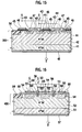
- an electric-field relaxation structure such as a first modification shown in a cross-sectional view of Fig. 4, which is a modification of the first embodiment, or a second modification shown in a cross-sectional view of Fig. 5, which is a modification of the first embodiment, can be provided, for example.
- the similar effect can be obtained as in the case of the configuration shown in Fig. 1.
- Fig. 4 shows a case where the end portions of the first hetero semiconductor region 3 are surmounted on interlayer dielectrics 7 comprised of SiO 2 , for example, stacked and formed on the end portions of the drift region 2.
- the formation of the end portions of the first hetero semiconductor region 3 on the interlayer dielectrics 7 provides various characteristics. The effect of an electric-field relaxation is obtained, and an etching damage is not easily incurred in the drift region 2 when the first hetero semiconductor region 3 is etched by dry etching, or the like.
- Fig. 4 shows a case where the interlayer dielectrics 7 are formed together with the electric-field relaxation regions 6.
- the semiconductor device can be configured such that only the interlayer dielectrics 7 exist.
- Fig. 5 shows a configuration in which adopted is a mesa structure formed with digging portions 8 formed by digging the end portions of the first hetero semiconductor region 3 and the drift region 2. With a structure like this, the field-electric relaxation of the junction ends can be also provided. In addition to the structure of Fig. 5, the electric-field relaxation regions 6 shown in Fig. 1 can be formed by being adjacent to the digging portions 8.
- the first hetero semiconductor regions 3 and the second hetero semiconductor regions 9 are formed one after another in a direction orthogonal to a direction in which the first semiconductor region 100 and the second semiconductor region 101 are stacked.
- the second semiconductor region 101 is formed such that the second hetero semiconductor region 9 is stacked on the first hetero semiconductor region 3.
- the conductivity type of the second hetero semiconductor region 9 can be either P-type or N-type, and the impurity density thereof can be either larger or smaller than that of the first hetero semiconductor region 3.
- the second hetero semiconductor region 9 is P-type in particular, and is higher in impurity density than the first hetero semiconductor region 3, an additional effect can be obtained as compared to the first embodiment.
- the resistance within the second semiconductor region 101 can be reduced while having a breakdown voltage on the same level as that of the configuration shown in Fig. 1. Further, when the impurity density of the second hetero semiconductor region 9 is so high as to ohmic contact with the anode electrode 4, the contact resistance therebetween can be also reduced. That is, an on-resistance at the time of forward direction conduction can be reduced. On the other hand, in the configuration shown in Fig. 7, the leakage current in a cutoff state can be reduced while having the on-resistance on the same level as the configuration shown in the first embodiment.
- Fig. 7 an explanation has been given of a case where the first hetero semiconductor region 3 and the second hetero semiconductor region 9 are formed, as separate regions, within the second semiconductor region 101.
- a fifth modification shown in a cross-sectional view of Fig. 17, which is a modification of the fourth modification, or a sixth modification shown in a cross-sectional view of Fig. 18, which is a modification of the fourth modification a configuration in which the second hetero semiconductor region 9 is deleted and a predetermined impurity density distribution is present in the first hetero semiconductor region 3 can be possible.
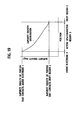
- Fig. 17 is a cross-sectional view corresponding to Fig. 1, in which the impurity density within the first hetero semiconductor region 3 is structured to have a predetermined gradient.
- Fig. 19 shows an impurity density distribution of the first hetero semiconductor region 3 along a line A-A in Fig. 17. As shown in Fig. 19, in the structure in Fig. 17, the impurity density within the hetero semiconductor region 3 is distributed such that a portion, within the first hetero semiconductor region 3, that contacts the anode electrode 4 is high in impurity density and a portion that contacts the drift region 2 is low in impurity density.
- the first semiconductor region 100 comprised of an N-type silicon carbide semiconductor base substrate formed such that the N - -type drift region 2 is epitaxially grown on the N + -type substrate region 1
- aluminum ions are selectively implanted into a predetermined drift region 2, for example, and thereafter, actively annealed to thereby form the P-type electric-field relaxation regions 6.
- Boron can be employed as an impurity used to form the electric-field relaxation regions 6.
- the electric-field relaxation regions 6 can be formed as high resistant regions in which to hold a breakdown voltage without activating the impurity, or formed of an insulating film such as an oxide film.
- the first hetero semiconductor region 3 can be formed by being stacked through an electron beam evaporation method or a sputtering method, and then, recrystallized by laser annealing or the like.
- the first hetero semiconductor region 3 can be formed of single crystal silicon heteroepitaxially grown by molecular beam epitaxy, for example.
- the doping is not only performed on the surface layer, but can be also performed by multi-step implantation to previously form a concentration distribution. Other doping methods can be employed.
- explanations have been given of a case where ions are directly implanted to the layer of the first hetero semiconductor region 3.
- a mask material is optionally formed by photolithography and etching, and by using reactive ion etching (dry etching) , for example, the first hetero semiconductor region 3 is selectively removed by using the previously formed mask material as a mask thereby to form a predetermined shape.
- Other masks such as an oxide film mask and a nitride film can be used for the mask material.
- the etching method other methods such as wet etching, for example, can be used.
- the second electrode 5 comprised of nickel (Ni) , for example, is formed, and in order to obtain a good contact resistance on the rear surface, a heat treatment at about 600 to 1200°C, for example, is applied thereto.
- a heat treatment at about 600 to 1200°C, for example, is applied thereto.
- the boronions simultaneously introduced in the first hetero semiconductor region 3 are impurity-activated so as to render P-type, and a predetermined impurity gradient is therein formed.
- titanium (Ti) and aluminum (Al) are stacked in this order to form the first electrode 4, whereby the semiconductor device shown in Fig. 17 is completed.
- the first hetero semiconductor region 3 was formed of polycrystalline silicon with a thickness of about 0.5 ⁇ m, and boron ions were implanted in the first hetero semiconductor region 3 up to about 0.1 ⁇ m deep from the surface layer. With this state, a heat treatment was applied. The experiment yielded the result that when a heat treatment was applied at 950°C for about 20 minutes, for example, the impurity distribution in the first hetero semiconductor region 3 was almost uniform. On the contrary, in a heat treatment at 900°C for about 1 minute, for example, it was confirmed that a concentration gradient of about half a digit was formed between the surface layer and the drift region 2 side.
- the use of the present manufacturing method provides a desired impurity density in each region by a single manufacturing process.
- the most ideal conditions for thus providing the gradient in the impurity distribution are set such that the impurity density on the side that contacts at least the drift region 2 of the first hetero semiconductor region 3 is equal to or less than an impurity density by which the avalanche breakdown occurs on the side of the first hetero semiconductor region 3 shown in the above Fig. 1, the impurity density on the side that contacts the first electrode 4 is equal to or more than the impurity density by which ohmic contact occurs, and the thickness of the first hetero semiconductor region 3 is the minimum.
- the use of the configuration of the sixth modification shown in Fig. 18 makes thin the thickness of the first hetero semiconductor region 3 and also provides a low on-resistance.
- Fig. 18 is a cross-sectional view corresponding to Fig. 17, in which the first hetero semiconductor region 3 is formed of a plurality of semiconductor layers (a lower semiconductor layer 13 and an upper semiconductor layer 14), and similar to the configuration of Fig. 17, the impurity density is configured to have a predetermined gradient.
- Fig. 18 shows a case where the first hetero semiconductor region 3 is formed of two semiconductor layers. However, the first hetero semiconductor region 3 can be formed of three or more layers.
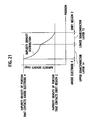
- Fig. 21 shows an impurity density distribution of the first hetero semiconductor region 3 along a line B-B in Fig. 18.
- the impurity density within the first hetero semiconductor region 3 is distributed and formed such that in a portion that contacts the anode electrode 4 within the first hetero semiconductor region 3 , the impurity density is high, and on the other hand, in a portion that contacts the drift region 2, the impurity density is low as compared to the portion that contacts the anode electrode 4.
- the gradient of the impurity is discontinuous, and a density difference of the impurity in terms of the entire first hetero semiconductor region 3 can be made larger than that of the configuration shown in Fig. 17.
- the configuration like this provides an effect similar to that of the fifth modification, and in addition, makes much thinner the thickness of the first hetero semiconductor region 3 as compared to that of the fifth modification, and reduces the on-resistance as well.
- This configuration can be easily achieved by using a manufacturing method shown below.
- the manufacturing method is explained with reference to a process cross-sectional view of Figs. 22A to 22C as an example.
- the first semiconductor region 100 comprised of an N-type silicon carbide semiconductor base substrate formed such that the N - -type drift region 2 is epitaxially grown on the N + -type substrate region 1
- aluminum ions are selectively implanted into a predetermined drift region 2, for example, and thereafter, actively annealed to thereby form the P-type electric-field relaxation regions 6.
- Boron can be used as an impurity to form the electric-field relaxation regions 6.
- the electric-field relaxation regions 6 can be formed as high resistant regions in which to hold a breakdown voltage without activating the impurity, or formed of an insulating film such as an oxide film.
- the lower semiconductor layer 13 comprised of polycrystalline silicon formed by an LP-CVD method is stacked on the drift region 2, and subsequently, on the lower semiconductor layer 13, the upper semiconductor layer 14 comprised of polycrystalline silicon formed by the LP-CVD method, for example, is stacked.
- the crystalline alignment of polycrystalline silicon formed between the lower semiconductor layer 13 and the upper semiconductor layer 14 are preferably at least discontinuous.
- formation temperatures can be made different so that the crystalline alignment is made discontinuous, or the both layers 13 and 14 can be separately formed.
- boron is doped by an ion-implantation method, for example, to form an implanted layer in a surface layer of the upper semiconductor layer 14 of the layer of the first hetero semiconductor region 3.
- the lower semiconductor layer 13 and the upper semiconductor layer 14 can be formed by being stacked through an electron beam evaporation method or a sputtering method, and then, recrystallized by laser annealing or the like.
- these layers 13 and 14 can be formed of single crystal silicon heteroepitaxially grown by molecular beam epitaxy, for example.
- the doping is not only applied to the surface layer, but also can be performed by multi-step implantation to previously form a concentration distribution. Other doping methods can be also employed.
- a mask material is optionally formed by photolithography and etching, and by using reactive ion etching (dry etching) , for example, the first hetero semiconductor region 3 is selectively removed by using the previously formed mask material as a mask to thereby form a predetermined shape.
- Other masks such as an oxide film mask and a nitride film can be used for the mask material.
- the etching method other methods such as wet etching, for example, can be used.
- the second electrode 5 comprised of nickel (Ni), for example, is formed, and in order to obtain a good contact resistance on the rear surface, a heat treatment at about 600 to 1200°C, for example, is applied thereto.
- the boron ions simultaneously introduced in the upper semiconductor layer 14 of the first hetero semiconductor region 3 are impurity-activated so as to render P-type, and a predetermined impurity gradient is therein formed.
- the first electrode 4 is formed by stacking titanium (Ti) and aluminum (Al) in this order, whereby the semiconductor device shown in Fig. 18 can be completed.
- the first hetero semiconductor region 3 was formed of polycrystalline silicon with a thickness of about 0.5 ⁇ m, and boron ions were implanted in the first hetero semiconductor region 3 up to about 0.1 ⁇ m deep from the surface layer. With this state, a heat treatment was applied. The experiment yielded the result that when a heat treatment was applied at 950°C for about 20 minutes, for example, the impurity distribution in the first hetero semiconductor region 3 was almost uni form . In contrary, in a heat treatment at 900°C for about 1 minute, for example, it was confirmed that a concentration gradient of about half a digit was formed between the surface layer and the drift region 2 side.
- the use of the present manufacturing method provides a desired impurity density in each region of a single manufacturing process.
- the semiconductor devices of the fifth modification shown in the Fig. 17 and the sixth modification shown in the Fig. 18 can be easily achieved by ingeniously applying the conventionally-known semiconductor manufacturing technique.
- Fig. 8 shows a case where the first electrode 4 of the heterojunction diode and Schottky electrode regions 10 of the Schottky junction diode are separately formed in different regions.
- Fig. 9 shows a case where the Schottky electrode region 10 serves also as the first electrode 4.
- an electrode material that causes the avalanche breakdown in the first hetero semiconductor region 3 can be used as a material of the Schottky electrode region 10 shown in Fig. 8 and Fig. 9.
- end portions of the first hetero semiconductor region 3 do not necessarily contact the electric-field relaxation regions 6.
- the electric field distribution is almost uniform also in the end portions of the first hetero semiconductor regions 3.
- the avalanche breakdown occurs on the entire junction surface between the drift region 2 and the first hetero semiconductor region 3, so that a high avalanche resistance can be obtained.
- Fig. 11 is a cross-sectional view showing a tenth modification of the first embodiment. There is shown a configuration in which the P-type regions 11 are discretely formed in the drift region 2, which are arranged additionally to the configuration shown in Fig. 7, and the P-type regions 11 are connected via the first hetero semiconductor region 3 to the first electrode 4.
- the impurity density and the depth are set such that the avalanche breakdown occurs in the first hetero semiconductor region 3.
- Figs. 10 and 11 an explanation is given of a case where the P-type regions 11 and the electric-field relaxation regions 6 differ in depth.
- the impurity density and the depth thereof can be equal.
- the end portions of the first hetero semiconductor region 3 do not necessarily contact the electric-field relaxation regions 6.
- the avalanche breakdown occurs on the entire junction surface between the drift region 2 and the first hetero semiconductor region 3, so that a high avalanche resistance can be obtained.
- a high electric field region 12 having a higher impurity density than the drift region 2 and more easily becoming a higher electric field than the surrounding areas, for example, canbe formed within the drift region 2 that contacts the first hetero semiconductor region 3.
- a higher electric field occurs in the high electric field region 12 as compared to at least the outer peripheral ends of the active region.
- the avalanche breakdown can be caused at the equal timing of or earlier than the outer peripheral ends in this region, and the similar effect can be obtained irrespective of the impurity density of the first hetero semiconductor region 3.
- the fact that when the impurity density of the first hetero semiconductor region 3 is adjusted, the dielectric breakdown electric field within the first hetero semiconductor region 3 can be controlled is focused, and the impurity density of the first hetero semiconductor region 3 is set to equal to or less than a predetermined value.
- the avalanche breakdown occurs at equal timing of or earlier than in the surrounding areas, such as end portions, of the drift region 2, in which the electric field reaches the maximum.
- the avalanche breakdown occurs almost uniformly on the entire junction surface that contacts the drift region 2.
- the avalanche resistance can be enhanced.
- Fig. 13 is a cross-sectional view showing the configuration of a semiconductor device according to a second embodiment of the present invention.
- a characteristic of the second embodiment shown in Fig. 13 is that the heterojunction diode having a high avalanche resistance, explained in the first embodiment including the first to eleventh modifications, is applied to a portion of a transistor.
- the semiconductor device of the second embodiment is configured such that an N - -type drift region 22 is formed on an N + -type substrate region 21 of which the polytype of silicon carbide is 4H, for example; and first hetero semiconductor regions 23 comprised of P-type polycrystalline silicon and second hetero semiconductor regions 24 comprised of N-type polycrystalline silicon are formed so as to contact a main surface that opposes the junction surface, of the drift region 22, with the substrate 21.
- a junction between the drift region 22, and the first and second hetero semiconductor regions 23 and 24 is formed by heterojunction comprised of a material of which band gap of the polycrystalline silicon is different from that of silicon carbide, and on the junction interface, an energetic barrier exists.
- Gate electrodes 26 formed so as to contact, via gate insulating films 25 comprised of a silicon oxide film, for example, the junction surface between the second hetero semiconductor region 24 and the drift region 22 ; a source electrode 27 formed so as to be connected to the second hetero semiconductor region 24 ; and a drain electrode 28 formed so as to be connected to the substrate region 1 are formed, respectively.
- Outer peripheral ends of the active region are formed with P-type electric-field relaxation regions 29, for example.
- the second embodiment is configured such that grooves are formed in the drift region 22 and the gate electrodes 26 are formed and buried in the grooves.
- a so-called planar configuration where no grooves are formed can be possible.
- the first hetero semiconductor regions 23 and the second hetero semiconductor region 24 are formed on the drift region 22.
- the first hetero semiconductor regions 23 and the second hetero semiconductor region 24 can be formed such that grooves are formed in predetermined regions of the drift region 22, for example, and these regions 23 and 24 are buried in the grooves.
- Fig. 13 shows a configuration in which the gate electrodes 26 and the second hetero semiconductor region 24 are contacted via the gate insulating films 25.
- Fig. 14 which is a modification of the second embodiment, the gate electrodes 26 and the first hetero semiconductor region 23 are connected via the gate insulating films 25, and the second hetero semiconductor region 24 needs not particularly be arranged.
- electric-field relaxation regions 29 are formed as structures formed in the outer peripheral ends of the active region.
- any configuration can be possible as long as a structure that can relax the electric field concentration of the outer peripheral ends is arranged.
- the gate electrodes 26 are ground electric potentials or negative electric potentials, for example, the cutoff state is held. This is due to the fact that on the heterojunction interface between the drift region 22, and the first and second hetero semiconductor regions 23 and 24, energetic barriers against conduction electrons are formed. At this time, as explained in the first embodiment, it is configured such that the leakage current is reduced when the carrier generated under a predetermined electric fieldbecomes the dominant cause. Thus, this configuration provides various effects, that is, a higher cutoff characteristic can be held, and a temperature characteristic of the leakage current is very small as well.
- an avalanche breakdown voltage caused between the first hetero semiconductor regions 23 and the drift region 22 is equivalent to, or equal to or less than the avalanche breakdown voltage occurring between the drift region 22 and the electric-field relaxation regions 29 formed at the outer peripheral ends of the active region. Therefore, the avalanche breakdown occurs in a wide range even in the main active region other than the outer peripheral ends of the active region. Thus, a high avalanche resistance can be achieved.
- the second embodiment can be implemented in a reverse conduction (a reflux operation) state where the source electrode 27 is grounded, andanegative electric potential is applied to the drain electrode 28, for example.
- a reverse conduction a reflux operation
- the source electrode 27 and the gate electrodes 26 are ground electric potentials and a predetermined positive electric potential is applied to the drain electrode 28, the energetic barrier against the conduction electrons disappear, and the conduction electrons pass from the side of the drift region 22 to the side of the first and second hetero semiconductor regions 23 and 24, resulting in the reverse conduction state.
- the conduction is established only by the conduction electrons without implantation of electron holes.
- loss caused by a reverse recovery current at the time of a change from the reverse conduction state to the cutoff state can be minimized.
- the gate electrodes 26 can be used as control electrodes, without being grounded.
- Fig. 15 shows the configuration of a semiconductor device in which a heterojunction diode is contained in a MOSFET comprised of silicon carbide.
- a first semiconductor region 300 comprised of a drift region 42 and a substrate region 41 of a first conductivity-type
- first conductivity-type source regions 43 and second conductivity-type base regions 44 are formed, and gate electrodes 46 are formed so as to contact the drift region 42, the base regions 44, and the source regions 43 via the gate insulating films 45.
- the base regions 44 and the source regions 43 are connected to source electrodes 47, and the substrate region 41 is connected to a drain electrode 48.
- the hetero semiconductor regions 49 are connected to the source electrodes 47.
- an electric-field relaxation region 50 is formed, for example.
- the avalanche breakdown occurs between the hetero semiconductor regions 49 and the drift region 42 when the heterojunction diode is changed f rom the conduction state to the cutoff state as a result of the application of the drain voltage of a predetermined value or more.
- the drain voltage of a predetermined value or more it becomes possible to pass a current in a wide range of the main region of the active region, so that a high avalanche resistance can be obtained.
- a configuration shown in Fig. 16 in which the heterojunction diode is contained in a JFET comprised of silicon carbide, too, the similar effect can be obtained as in the configuration shown in Fig. 15.
- a first semiconductor region 400 comprised of a drift region 52 and a substrate region 51 of a first conductivity-type
- the gate regions 54 are connected to gate electrodes 55
- the source regions 53 are connected to source electrodes 56
- the substrate region 51 is connected to a drain electrode 57.
- Hetero semiconductor regions 58 having a band gap different from that of the drift region 52 and comprised of polycrystalline silicon, for example, are arranged so as to form heterojunction with the drift region 52.
- the source regions 53 and the hetero semiconductor regions 58 are formed in a depth direction of the drawing one after another, and the hetero semiconductor regions 58 are connected to the source electrodes 56.
- an electric-field relaxation region 59 is formed, for example.
- the avalanche breakdown occurs between the hetero semiconductor regions 58 and the drift region 52 when the heterojunction diode is changed from the conduction state to the cutoff state as a result of the application of the drain voltage of a predetermined value or more.
- the drain voltage of a predetermined value or more it becomes possible to pass a current in a wide range of the main region of the active region, so that a high avalanche resistance can be obtained.
- the semiconductor device of which substrate material is silicon carbide as an example can include other semiconductor materials such as silicon, silicon germanium, gallium nitride, and diamond.
- substrate material can include other semiconductor materials such as silicon, silicon germanium, gallium nitride, and diamond.
- the polytype of silicon carbide is 4H.
- other polytypes such as 6H, and 3C can be also adopted.
- the semiconductor device can be also a transistor or so-called horizontally structured diode, in which the second electrode 5 (drain electrodes 28, 48, and 57) and the first electrode 4 (source electrodes 27, 47, and 56) are arranged on the same main surface, and a current is passed in a horizontal direction.
- any combination such as a combination between N-type silicon carbide and P-type polycrystalline silicon, a combination between P-type silicon carbide and P-type polycrystalline silicon, and a combination between P-type silicon carbide and N-type polycrystalline silicon can be used.
- the present invention it becomes possible to cause avalanche breakdown at an equal timing of or earlier than at outer peripheral ends in an entire junction surface of a heterojunction region other than outer peripheral ends of a heterojunction diode. Thereby, an avalanche resistance can be enhanced.
Landscapes
- Electrodes Of Semiconductors (AREA)
- Bipolar Transistors (AREA)
Applications Claiming Priority (2)
| Application Number | Priority Date | Filing Date | Title |
|---|---|---|---|
| JP2006108557 | 2006-04-11 | ||
| JP2007024314A JP5560519B2 (ja) | 2006-04-11 | 2007-02-02 | 半導体装置及びその製造方法 |
Publications (3)
| Publication Number | Publication Date |
|---|---|
| EP1845561A2 true EP1845561A2 (fr) | 2007-10-17 |
| EP1845561A3 EP1845561A3 (fr) | 2009-12-30 |
| EP1845561B1 EP1845561B1 (fr) | 2017-03-08 |
Family
ID=38235304
Family Applications (1)
| Application Number | Title | Priority Date | Filing Date |
|---|---|---|---|
| EP07007103.0A Active EP1845561B1 (fr) | 2006-04-11 | 2007-04-04 | Dispositif de semi-conducteurs comprenant une diode à hétérojonction et son procédé de fabrication |
Country Status (5)
| Country | Link |
|---|---|
| US (1) | US7781786B2 (fr) |
| EP (1) | EP1845561B1 (fr) |
| JP (1) | JP5560519B2 (fr) |
| KR (1) | KR100937276B1 (fr) |
| CN (1) | CN101055894B (fr) |
Cited By (28)
| Publication number | Priority date | Publication date | Assignee | Title |
|---|---|---|---|---|
| WO2010141146A1 (fr) * | 2009-06-03 | 2010-12-09 | Cree, Inc. | Diodes schottky comprenant du poly-silicium à faibles hauteurs de barrière et leurs procédés de fabrication |
| US8193848B2 (en) | 2009-06-02 | 2012-06-05 | Cree, Inc. | Power switching devices having controllable surge current capabilities |
| US8294507B2 (en) | 2009-05-08 | 2012-10-23 | Cree, Inc. | Wide bandgap bipolar turn-off thyristor having non-negative temperature coefficient and related control circuits |
| US8330244B2 (en) | 2006-08-01 | 2012-12-11 | Cree, Inc. | Semiconductor devices including Schottky diodes having doped regions arranged as islands and methods of fabricating same |
| US8354690B2 (en) | 2009-08-31 | 2013-01-15 | Cree, Inc. | Solid-state pinch off thyristor circuits |
| WO2013036641A1 (fr) | 2011-09-09 | 2013-03-14 | Cree, Inc. | Dispositifs à semi-conducteur à zones barrières non implantées et procédés de fabrication correspondants |
| US8415671B2 (en) | 2010-04-16 | 2013-04-09 | Cree, Inc. | Wide band-gap MOSFETs having a heterojunction under gate trenches thereof and related methods of forming such devices |
| US8432012B2 (en) | 2006-08-01 | 2013-04-30 | Cree, Inc. | Semiconductor devices including schottky diodes having overlapping doped regions and methods of fabricating same |
| US8541787B2 (en) | 2009-07-15 | 2013-09-24 | Cree, Inc. | High breakdown voltage wide band-gap MOS-gated bipolar junction transistors with avalanche capability |
| EP2443659A4 (fr) * | 2009-06-19 | 2013-11-20 | Power Integrations Inc | Transistors à effet de champ à jonction verticale et diodes ayant des régions à gradient et procédés de fabrication |
| US8618582B2 (en) | 2011-09-11 | 2013-12-31 | Cree, Inc. | Edge termination structure employing recesses for edge termination elements |
| US8629509B2 (en) | 2009-06-02 | 2014-01-14 | Cree, Inc. | High voltage insulated gate bipolar transistors with minority carrier diverter |
| US8653534B2 (en) | 2008-05-21 | 2014-02-18 | Cree, Inc. | Junction Barrier Schottky diodes with current surge capability |
| US8664665B2 (en) | 2011-09-11 | 2014-03-04 | Cree, Inc. | Schottky diode employing recesses for elements of junction barrier array |
| US8680587B2 (en) | 2011-09-11 | 2014-03-25 | Cree, Inc. | Schottky diode |
| US8710510B2 (en) | 2006-08-17 | 2014-04-29 | Cree, Inc. | High power insulated gate bipolar transistors |
| US8835987B2 (en) | 2007-02-27 | 2014-09-16 | Cree, Inc. | Insulated gate bipolar transistors including current suppressing layers |
| US9029945B2 (en) | 2011-05-06 | 2015-05-12 | Cree, Inc. | Field effect transistor devices with low source resistance |
| US9117739B2 (en) | 2010-03-08 | 2015-08-25 | Cree, Inc. | Semiconductor devices with heterojunction barrier regions and methods of fabricating same |
| US9142662B2 (en) | 2011-05-06 | 2015-09-22 | Cree, Inc. | Field effect transistor devices with low source resistance |
| EP2911205A4 (fr) * | 2012-10-19 | 2016-03-02 | Nissan Motor | Dispositif semi-conducteur et son procédé de fabrication |
| US9373617B2 (en) | 2011-09-11 | 2016-06-21 | Cree, Inc. | High current, low switching loss SiC power module |
| EP3051593A1 (fr) * | 2015-01-30 | 2016-08-03 | Nxp B.V. | Dispositif semi-conducteur |
| US9640617B2 (en) | 2011-09-11 | 2017-05-02 | Cree, Inc. | High performance power module |
| US9673283B2 (en) | 2011-05-06 | 2017-06-06 | Cree, Inc. | Power module for supporting high current densities |
| EP2565922A4 (fr) * | 2010-04-28 | 2017-11-29 | Nissan Motor Co., Ltd | Dispositif semiconducteur |
| EP3726586A4 (fr) * | 2017-12-14 | 2021-07-21 | Shindengen Electric Manufacturing Co., Ltd. | Dispositif à semi-conducteur à large bande interdite |
| US11355630B2 (en) | 2020-09-11 | 2022-06-07 | Wolfspeed, Inc. | Trench bottom shielding methods and approaches for trenched semiconductor device structures |
Families Citing this family (37)
| Publication number | Priority date | Publication date | Assignee | Title |
|---|---|---|---|---|
| JP5341373B2 (ja) * | 2008-03-12 | 2013-11-13 | セミコンダクター・コンポーネンツ・インダストリーズ・リミテッド・ライアビリティ・カンパニー | ダイオード |
| JP5808516B2 (ja) * | 2009-03-02 | 2015-11-10 | 日産自動車株式会社 | 半導体装置 |
| JP5476743B2 (ja) * | 2009-03-04 | 2014-04-23 | 日産自動車株式会社 | 半導体装置 |
| JP5439873B2 (ja) * | 2009-03-09 | 2014-03-12 | 日産自動車株式会社 | 半導体装置 |
| JP5402232B2 (ja) * | 2009-05-19 | 2014-01-29 | 日産自動車株式会社 | 半導体装置 |
| JP5439215B2 (ja) | 2010-02-10 | 2014-03-12 | 株式会社東芝 | 半導体装置および半導体装置の製造方法 |
| JP5598015B2 (ja) * | 2010-02-23 | 2014-10-01 | 株式会社デンソー | ショットキーバリアダイオードを備えた炭化珪素半導体装置およびその製造方法 |
| IT1401754B1 (it) | 2010-08-30 | 2013-08-02 | St Microelectronics Srl | Dispositivo elettronico integrato e relativo metodo di fabbricazione. |
| IT1401756B1 (it) | 2010-08-30 | 2013-08-02 | St Microelectronics Srl | Dispositivo elettronico integrato con struttura di terminazione di bordo e relativo metodo di fabbricazione. |
| IT1401755B1 (it) * | 2010-08-30 | 2013-08-02 | St Microelectronics Srl | Dispositivo elettronico integrato a conduzione verticale e relativo metodo di fabbricazione. |
| US8389348B2 (en) * | 2010-09-14 | 2013-03-05 | Taiwan Semiconductor Manufacturing Company, Ltd. | Mechanism of forming SiC crystalline on Si substrates to allow integration of GaN and Si electronics |
| CN103370791B (zh) * | 2011-03-14 | 2016-09-14 | 富士电机株式会社 | 半导体器件 |
| JPWO2012157679A1 (ja) * | 2011-05-18 | 2014-07-31 | ローム株式会社 | 半導体装置およびその製造方法 |
| JP5464192B2 (ja) * | 2011-09-29 | 2014-04-09 | 株式会社デンソー | 半導体装置の製造方法 |
| US8969994B2 (en) * | 2012-08-14 | 2015-03-03 | Avogy, Inc. | Method of fabricating a gallium nitride merged P-i-N Schottky (MPS) diode by regrowth and etch back |
| US9064887B2 (en) | 2012-09-04 | 2015-06-23 | Infineon Technologies Austria Ag | Field-effect semiconductor device and manufacturing method therefor |
| KR102011174B1 (ko) | 2012-09-27 | 2019-08-14 | 로무 가부시키가이샤 | 칩 다이오드 및 그 제조 방법 |
| JP6082229B2 (ja) * | 2012-10-30 | 2017-02-15 | 住友化学株式会社 | 窒化物半導体素子およびその製造方法 |
| US9331197B2 (en) | 2013-08-08 | 2016-05-03 | Cree, Inc. | Vertical power transistor device |
| US10600903B2 (en) | 2013-09-20 | 2020-03-24 | Cree, Inc. | Semiconductor device including a power transistor device and bypass diode |
| US20150084063A1 (en) * | 2013-09-20 | 2015-03-26 | Cree, Inc. | Semiconductor device with a current spreading layer |
| US10868169B2 (en) * | 2013-09-20 | 2020-12-15 | Cree, Inc. | Monolithically integrated vertical power transistor and bypass diode |
| JP5735611B2 (ja) * | 2013-11-01 | 2015-06-17 | ローム株式会社 | SiC半導体装置 |
| JP6305751B2 (ja) * | 2013-12-16 | 2018-04-04 | 新日本無線株式会社 | ショットキーダイオードとその製造方法 |
| JP6329054B2 (ja) * | 2014-10-10 | 2018-05-23 | トヨタ自動車株式会社 | スイッチング回路 |
| CN106169417A (zh) * | 2016-07-11 | 2016-11-30 | 厦门市三安集成电路有限公司 | 一种异质结终端的碳化硅功率器件及其制备方法 |
| KR102016447B1 (ko) * | 2017-04-17 | 2019-08-30 | 한국전기연구원 | 폴리실리콘을 이용한 실리콘카바이드 트렌치 쇼트키 배리어 다이오드의 제조방법 |
| CN107238786B (zh) * | 2017-04-24 | 2019-10-25 | 中国科学院微电子研究所 | 用于mosfet器件模型参数提取的方法及装置 |
| CN111386606A (zh) | 2018-01-18 | 2020-07-07 | 英特尔公司 | 堆叠晶体管架构中的垂直二极管 |
| KR102097711B1 (ko) * | 2018-05-24 | 2020-04-06 | 한국전기연구원 | 실리콘카바이드 트렌치 쇼트키 배리어 다이오드 및 이의 제조방법 |
| JP2020092282A (ja) * | 2020-02-25 | 2020-06-11 | ローム株式会社 | ショットキーバリアダイオード |
| CN113871488A (zh) * | 2021-09-28 | 2021-12-31 | 西安电子科技大学 | 一种复合结构的垂直氧化镓异质结二极管及其制作方法 |
| CN117316766A (zh) * | 2023-11-29 | 2023-12-29 | 深圳基本半导体有限公司 | 一种碳化硅二极管器件的制备方法及器件 |
| CN119208137B (zh) * | 2024-06-27 | 2025-11-04 | 长飞先进半导体(武汉)有限公司 | 功率器件及制备方法、功率模块、功率转换电路和车辆 |
| CN118658783B (zh) * | 2024-06-27 | 2025-02-07 | 长飞先进半导体(武汉)有限公司 | 功率器件及制备方法、功率模块、功率转换电路和车辆 |
| CN118610092B (zh) * | 2024-06-27 | 2025-08-26 | 长飞先进半导体(武汉)有限公司 | 功率器件及制备方法、功率模块、功率转换电路和车辆 |
| CN118610093A (zh) * | 2024-06-27 | 2024-09-06 | 长飞先进半导体(武汉)有限公司 | 功率器件及制备方法、功率模块、功率转换电路和车辆 |
Family Cites Families (26)
| Publication number | Priority date | Publication date | Assignee | Title |
|---|---|---|---|---|
| GB1393536A (en) * | 1971-07-28 | 1975-05-07 | Mullard Ltd | Electroluminescent semiconductor devices |
| US5168328A (en) * | 1990-07-03 | 1992-12-01 | Litton Systems, Inc. | Heterojunction impatt diode |
| JPH0669222A (ja) | 1992-08-17 | 1994-03-11 | Matsushita Electric Ind Co Ltd | ヘテロ接合バイポーラトランジスタ及びその製造方法 |
| JP3529460B2 (ja) * | 1994-12-01 | 2004-05-24 | 株式会社東芝 | 液晶表示装置 |
| US5739554A (en) * | 1995-05-08 | 1998-04-14 | Cree Research, Inc. | Double heterojunction light emitting diode with gallium nitride active layer |
| JP3461274B2 (ja) | 1996-10-16 | 2003-10-27 | 株式会社東芝 | 半導体装置 |
| US6774449B1 (en) * | 1999-09-16 | 2004-08-10 | Matsushita Electric Industrial Co., Ltd. | Semiconductor device and method for fabricating the same |
| JP4126872B2 (ja) * | 2000-12-12 | 2008-07-30 | サンケン電気株式会社 | 定電圧ダイオード |
| KR100375829B1 (ko) | 2000-12-19 | 2003-03-15 | 한국전자통신연구원 | 아발란치 광 검출기 |
| JP4220683B2 (ja) * | 2001-03-27 | 2009-02-04 | パナソニック株式会社 | 半導体装置 |
| US6939730B2 (en) * | 2001-04-24 | 2005-09-06 | Sony Corporation | Nitride semiconductor, semiconductor device, and method of manufacturing the same |
| US6552363B2 (en) | 2001-09-18 | 2003-04-22 | International Rectifier Corporation | Polysilicon FET built on silicon carbide diode substrate |
| US7183575B2 (en) * | 2002-02-19 | 2007-02-27 | Nissan Motor Co., Ltd. | High reverse voltage silicon carbide diode and method of manufacturing the same high reverse voltage silicon carbide diode |
| JP4282972B2 (ja) * | 2002-02-19 | 2009-06-24 | 日産自動車株式会社 | 高耐圧ダイオード |
| US20050045982A1 (en) * | 2002-03-22 | 2005-03-03 | Krishna Shenai | Semiconductor device with novel junction termination |
| JP4463482B2 (ja) * | 2002-07-11 | 2010-05-19 | パナソニック株式会社 | Misfet及びその製造方法 |
| US7217950B2 (en) * | 2002-10-11 | 2007-05-15 | Nissan Motor Co., Ltd. | Insulated gate tunnel-injection device having heterojunction and method for manufacturing the same |
| JP4385206B2 (ja) * | 2003-01-07 | 2009-12-16 | 日本電気株式会社 | 電界効果トランジスタ |
| US20050012143A1 (en) * | 2003-06-24 | 2005-01-20 | Hideaki Tanaka | Semiconductor device and method of manufacturing the same |
| JP4211642B2 (ja) * | 2004-03-09 | 2009-01-21 | 日産自動車株式会社 | 半導体装置 |
| US7138668B2 (en) * | 2003-07-30 | 2006-11-21 | Nissan Motor Co., Ltd. | Heterojunction diode with reduced leakage current |
| JP5216183B2 (ja) | 2004-04-13 | 2013-06-19 | 日産自動車株式会社 | 半導体装置 |
| US20060060917A1 (en) * | 2004-09-17 | 2006-03-23 | Nissan Motor Co., Ltd. | Semiconductor device and method of manufacturing semiconductor device |
| JP5011681B2 (ja) * | 2004-12-02 | 2012-08-29 | 日産自動車株式会社 | 半導体装置 |
| US7368762B2 (en) * | 2005-01-06 | 2008-05-06 | Teledyne Licensing, Llc | Heterojunction photodiode |
| JP4948784B2 (ja) * | 2005-05-19 | 2012-06-06 | 三菱電機株式会社 | 半導体装置及びその製造方法 |
-
2007
- 2007-02-02 JP JP2007024314A patent/JP5560519B2/ja not_active Expired - Fee Related
- 2007-04-04 EP EP07007103.0A patent/EP1845561B1/fr active Active
- 2007-04-10 KR KR1020070035093A patent/KR100937276B1/ko not_active Expired - Fee Related
- 2007-04-10 US US11/783,577 patent/US7781786B2/en active Active
- 2007-04-11 CN CN2007100905757A patent/CN101055894B/zh active Active
Cited By (43)
| Publication number | Priority date | Publication date | Assignee | Title |
|---|---|---|---|---|
| US8330244B2 (en) | 2006-08-01 | 2012-12-11 | Cree, Inc. | Semiconductor devices including Schottky diodes having doped regions arranged as islands and methods of fabricating same |
| US8432012B2 (en) | 2006-08-01 | 2013-04-30 | Cree, Inc. | Semiconductor devices including schottky diodes having overlapping doped regions and methods of fabricating same |
| US9548374B2 (en) | 2006-08-17 | 2017-01-17 | Cree, Inc. | High power insulated gate bipolar transistors |
| US8710510B2 (en) | 2006-08-17 | 2014-04-29 | Cree, Inc. | High power insulated gate bipolar transistors |
| US9064840B2 (en) | 2007-02-27 | 2015-06-23 | Cree, Inc. | Insulated gate bipolar transistors including current suppressing layers |
| US8835987B2 (en) | 2007-02-27 | 2014-09-16 | Cree, Inc. | Insulated gate bipolar transistors including current suppressing layers |
| US8653534B2 (en) | 2008-05-21 | 2014-02-18 | Cree, Inc. | Junction Barrier Schottky diodes with current surge capability |
| US8294507B2 (en) | 2009-05-08 | 2012-10-23 | Cree, Inc. | Wide bandgap bipolar turn-off thyristor having non-negative temperature coefficient and related control circuits |
| US8629509B2 (en) | 2009-06-02 | 2014-01-14 | Cree, Inc. | High voltage insulated gate bipolar transistors with minority carrier diverter |
| US8193848B2 (en) | 2009-06-02 | 2012-06-05 | Cree, Inc. | Power switching devices having controllable surge current capabilities |
| US8304783B2 (en) | 2009-06-03 | 2012-11-06 | Cree, Inc. | Schottky diodes including polysilicon having low barrier heights and methods of fabricating the same |
| WO2010141146A1 (fr) * | 2009-06-03 | 2010-12-09 | Cree, Inc. | Diodes schottky comprenant du poly-silicium à faibles hauteurs de barrière et leurs procédés de fabrication |
| EP2443659A4 (fr) * | 2009-06-19 | 2013-11-20 | Power Integrations Inc | Transistors à effet de champ à jonction verticale et diodes ayant des régions à gradient et procédés de fabrication |
| US8541787B2 (en) | 2009-07-15 | 2013-09-24 | Cree, Inc. | High breakdown voltage wide band-gap MOS-gated bipolar junction transistors with avalanche capability |
| US8354690B2 (en) | 2009-08-31 | 2013-01-15 | Cree, Inc. | Solid-state pinch off thyristor circuits |
| US9595618B2 (en) | 2010-03-08 | 2017-03-14 | Cree, Inc. | Semiconductor devices with heterojunction barrier regions and methods of fabricating same |
| US9117739B2 (en) | 2010-03-08 | 2015-08-25 | Cree, Inc. | Semiconductor devices with heterojunction barrier regions and methods of fabricating same |
| US8415671B2 (en) | 2010-04-16 | 2013-04-09 | Cree, Inc. | Wide band-gap MOSFETs having a heterojunction under gate trenches thereof and related methods of forming such devices |
| EP2565922A4 (fr) * | 2010-04-28 | 2017-11-29 | Nissan Motor Co., Ltd | Dispositif semiconducteur |
| US9142662B2 (en) | 2011-05-06 | 2015-09-22 | Cree, Inc. | Field effect transistor devices with low source resistance |
| US9673283B2 (en) | 2011-05-06 | 2017-06-06 | Cree, Inc. | Power module for supporting high current densities |
| US9029945B2 (en) | 2011-05-06 | 2015-05-12 | Cree, Inc. | Field effect transistor devices with low source resistance |
| WO2013036641A1 (fr) | 2011-09-09 | 2013-03-14 | Cree, Inc. | Dispositifs à semi-conducteur à zones barrières non implantées et procédés de fabrication correspondants |
| EP2754182A4 (fr) * | 2011-09-09 | 2015-04-22 | Cree Inc | Dispositifs à semi-conducteur à zones barrières non implantées et procédés de fabrication correspondants |
| US9865750B2 (en) | 2011-09-11 | 2018-01-09 | Cree, Inc. | Schottky diode |
| US10141302B2 (en) | 2011-09-11 | 2018-11-27 | Cree, Inc. | High current, low switching loss SiC power module |
| US11171229B2 (en) | 2011-09-11 | 2021-11-09 | Cree, Inc. | Low switching loss high performance power module |
| US9231122B2 (en) | 2011-09-11 | 2016-01-05 | Cree, Inc. | Schottky diode |
| US11024731B2 (en) | 2011-09-11 | 2021-06-01 | Cree, Inc. | Power module for supporting high current densities |
| US9640617B2 (en) | 2011-09-11 | 2017-05-02 | Cree, Inc. | High performance power module |
| US8680587B2 (en) | 2011-09-11 | 2014-03-25 | Cree, Inc. | Schottky diode |
| US10153364B2 (en) | 2011-09-11 | 2018-12-11 | Cree, Inc. | Power module having a switch module for supporting high current densities |
| US9373617B2 (en) | 2011-09-11 | 2016-06-21 | Cree, Inc. | High current, low switching loss SiC power module |
| US8664665B2 (en) | 2011-09-11 | 2014-03-04 | Cree, Inc. | Schottky diode employing recesses for elements of junction barrier array |
| US8618582B2 (en) | 2011-09-11 | 2013-12-31 | Cree, Inc. | Edge termination structure employing recesses for edge termination elements |
| EP2911205A4 (fr) * | 2012-10-19 | 2016-03-02 | Nissan Motor | Dispositif semi-conducteur et son procédé de fabrication |
| US9735290B2 (en) | 2015-01-30 | 2017-08-15 | Nexperia B.V. | Semiconductor device |
| EP3051593A1 (fr) * | 2015-01-30 | 2016-08-03 | Nxp B.V. | Dispositif semi-conducteur |
| EP3726586A4 (fr) * | 2017-12-14 | 2021-07-21 | Shindengen Electric Manufacturing Co., Ltd. | Dispositif à semi-conducteur à large bande interdite |
| US11342435B2 (en) | 2017-12-14 | 2022-05-24 | Shindengen Electric Manufacturing Co., Ltd. | Wide-gap semiconductor device |
| US11355630B2 (en) | 2020-09-11 | 2022-06-07 | Wolfspeed, Inc. | Trench bottom shielding methods and approaches for trenched semiconductor device structures |
| WO2022056076A3 (fr) * | 2020-09-11 | 2022-07-07 | Cree, Inc. | Approches et procédés de blindage de fond de tranchée pour structures de dispositif à semi-conducteur à tranchée |
| US12279448B2 (en) | 2020-09-11 | 2025-04-15 | Wolfspeed, Inc. | Trench bottom shielding methods and approaches for trenched semiconductor device structures |
Also Published As
| Publication number | Publication date |
|---|---|
| CN101055894A (zh) | 2007-10-17 |
| US7781786B2 (en) | 2010-08-24 |
| CN101055894B (zh) | 2012-05-30 |
| EP1845561B1 (fr) | 2017-03-08 |
| EP1845561A3 (fr) | 2009-12-30 |
| KR100937276B1 (ko) | 2010-01-18 |
| US20070235745A1 (en) | 2007-10-11 |
| JP2007305964A (ja) | 2007-11-22 |
| KR20070101156A (ko) | 2007-10-16 |
| JP5560519B2 (ja) | 2014-07-30 |
Similar Documents
| Publication | Publication Date | Title |
|---|---|---|
| EP1845561B1 (fr) | Dispositif de semi-conducteurs comprenant une diode à hétérojonction et son procédé de fabrication | |
| US11961904B2 (en) | Semiconductor device including trench gate structure and buried shielding region and method of manufacturing | |
| EP1503425B1 (fr) | Dispositif semi-conducteur à hétérojonction et procédé pour sa fabrication | |
| KR102204272B1 (ko) | 게이트 트렌치들 및 매립된 종단 구조체들을 갖는 전력 반도체 디바이스들 및 관련 방법들 | |
| KR101630895B1 (ko) | 전류 시프팅 영역들을 갖는 반도체 장치들 및 관련 방법들 | |
| KR101494935B1 (ko) | 메사 스텝들을 포함하는 버퍼층들 및 메사 구조들을 가지는 전력 반도체 장치들 | |
| EP2710635B1 (fr) | Dispositifs en sic à tension de blocage élevée et à terminaison en biseau négatif | |
| TWI422029B (zh) | 具有抑制少數載體射入之碳化矽接合障礙蕭特基二極體 | |
| JP5554042B2 (ja) | ジャンクション・バリア・ショットキ・ダイオードに関する方法と、そのダイオードおよびその使用方法 | |
| EP4235798A2 (fr) | Diodes schottky et procédé permettant de fabriquer ces dernières | |
| KR101012532B1 (ko) | 반도체 장치 및 그 제조 방법 | |
| EP3117463B1 (fr) | Structure igbt pour matériaux semi-conducteurs à large bande interdite | |
| WO2023183215A1 (fr) | Structures de protection de support pour des dispositifs à semi-conducteur à tranchées | |
| US11222973B2 (en) | Semiconductor device | |
| US9349797B2 (en) | SiC devices with high blocking voltage terminated by a negative bevel | |
| EP1882273A2 (fr) | Dispositifs bipolaires mos carbure de silicium haute tension possedant des capacites de blocage bidirectionnelles et procedes de fabrication de ceux-ci | |
| JP3998454B2 (ja) | 電力用半導体装置 | |
| JP2004528728A5 (fr) | ||
| WO2013119548A1 (fr) | Dispositifs au sic avec haute tension de blocage terminé par un biseau négatif | |
| EP0890183B1 (fr) | TRANSISTOR A EFFET DE CHAMP EN SiC ET SON PROCEDE DE PRODUCTION |
Legal Events
| Date | Code | Title | Description |
|---|---|---|---|
| PUAI | Public reference made under article 153(3) epc to a published international application that has entered the european phase |
Free format text: ORIGINAL CODE: 0009012 |
|
| 17P | Request for examination filed |
Effective date: 20070816 |
|
| AK | Designated contracting states |
Kind code of ref document: A2 Designated state(s): AT BE BG CH CY CZ DE DK EE ES FI FR GB GR HU IE IS IT LI LT LU LV MC MT NL PL PT RO SE SI SK TR |
|
| AX | Request for extension of the european patent |
Extension state: AL BA HR MK YU |
|
| PUAL | Search report despatched |
Free format text: ORIGINAL CODE: 0009013 |
|
| AK | Designated contracting states |
Kind code of ref document: A3 Designated state(s): AT BE BG CH CY CZ DE DK EE ES FI FR GB GR HU IE IS IT LI LT LU LV MC MT NL PL PT RO SE SI SK TR |
|
| AX | Request for extension of the european patent |
Extension state: AL BA HR MK RS |
|
| AKX | Designation fees paid |
Designated state(s): DE FR GB |
|
| 17Q | First examination report despatched |
Effective date: 20110815 |
|
| GRAP | Despatch of communication of intention to grant a patent |
Free format text: ORIGINAL CODE: EPIDOSNIGR1 |
|
| INTG | Intention to grant announced |
Effective date: 20161110 |
|
| GRAS | Grant fee paid |
Free format text: ORIGINAL CODE: EPIDOSNIGR3 |
|
| GRAA | (expected) grant |
Free format text: ORIGINAL CODE: 0009210 |
|
| AK | Designated contracting states |
Kind code of ref document: B1 Designated state(s): DE FR GB |
|
| REG | Reference to a national code |
Ref country code: GB Ref legal event code: FG4D |
|
| REG | Reference to a national code |
Ref country code: DE Ref legal event code: R096 Ref document number: 602007050043 Country of ref document: DE |
|
| REG | Reference to a national code |
Ref country code: FR Ref legal event code: PLFP Year of fee payment: 11 |
|
| REG | Reference to a national code |
Ref country code: DE Ref legal event code: R097 Ref document number: 602007050043 Country of ref document: DE |
|
| PLBE | No opposition filed within time limit |
Free format text: ORIGINAL CODE: 0009261 |
|
| STAA | Information on the status of an ep patent application or granted ep patent |
Free format text: STATUS: NO OPPOSITION FILED WITHIN TIME LIMIT |
|
| 26N | No opposition filed |
Effective date: 20171211 |
|
| REG | Reference to a national code |
Ref country code: FR Ref legal event code: PLFP Year of fee payment: 12 |
|
| REG | Reference to a national code |
Ref country code: DE Ref legal event code: R079 Ref document number: 602007050043 Country of ref document: DE Free format text: PREVIOUS MAIN CLASS: H01L0029861000 Ipc: H10D0008000000 |
|
| PGFP | Annual fee paid to national office [announced via postgrant information from national office to epo] |
Ref country code: FR Payment date: 20250319 Year of fee payment: 19 |
|
| PGFP | Annual fee paid to national office [announced via postgrant information from national office to epo] |
Ref country code: GB Payment date: 20250319 Year of fee payment: 19 |
|
| PGFP | Annual fee paid to national office [announced via postgrant information from national office to epo] |
Ref country code: DE Payment date: 20250319 Year of fee payment: 19 |