EP1848099A1 - Ensemble de circuit et procédé pour le fonctionnement d' au moins une charge - Google Patents
Ensemble de circuit et procédé pour le fonctionnement d' au moins une charge Download PDFInfo
- Publication number
- EP1848099A1 EP1848099A1 EP06008130A EP06008130A EP1848099A1 EP 1848099 A1 EP1848099 A1 EP 1848099A1 EP 06008130 A EP06008130 A EP 06008130A EP 06008130 A EP06008130 A EP 06008130A EP 1848099 A1 EP1848099 A1 EP 1848099A1
- Authority
- EP
- European Patent Office
- Prior art keywords
- boost converter
- circuit arrangement
- switch
- supply voltage
- current
- Prior art date
- Legal status (The legal status is an assumption and is not a legal conclusion. Google has not performed a legal analysis and makes no representation as to the accuracy of the status listed.)
- Withdrawn
Links
Images


Classifications
-
- G—PHYSICS
- G05—CONTROLLING; REGULATING
- G05F—SYSTEMS FOR REGULATING ELECTRIC OR MAGNETIC VARIABLES
- G05F1/00—Automatic systems in which deviations of an electric quantity from one or more predetermined values are detected at the output of the system and fed back to a device within the system to restore the detected quantity to its predetermined value or values, i.e. retroactive systems
- G05F1/70—Regulating power factor; Regulating reactive current or power
Definitions
- the present invention relates to a circuit arrangement for operating at least one consumer, comprising a supply voltage connection for connecting a supply voltage, a step-up converter which is coupled to the supply voltage terminal, wherein the boost converter comprises a boost converter inductor, an electronic boost converter switch, a boost converter diode and a boost converter capacitor, and an output terminal for connecting the at least one consumer. It also relates to a method for operating at least one consumer on such a circuit arrangement.
- FIG. 1 To illustrate the problem underlying the invention, reference is first made to the circuit arrangement shown in FIG. 1, known from the prior art.
- This circuit has a supply voltage terminal to which a mains voltage U N is connected.
- the current flowing from the network into the circuit is denoted by IN.
- a filter unit comprising a capacitor C1 and two coils L1a and L1b coupled together prevents the transmission of disturbances from the circuit to the network.
- the filter unit is followed by a rectifier comprising diodes D1, D2, D3 and D4.
- the rectified filtered mains voltage U NG is provided to a boost converter by a capacitor C2, which comprises a boost converter inductor L2a, an electronic boost converter switch T1, a boost converter diode D5, and a boost converter capacitor C3.
- a control device 10 For the evaluation of the current through the inductor L2b serves - among other functions - a control device 10.
- a shunt resistor R1 for measurement of the current through the boost converter switch T1 via the input 16 of the control device 10 is provided.
- the voltage drop across the capacitor C3 is usually referred to as intermediate circuit voltage U ZK and provided via an output terminal A1, A2 to a consumer, not shown.
- the consumer may be a lamp, for example.
- the intermediate circuit voltage U ZK is regulated by the control device 10 and therefore supplied to it via an input 18.
- the control device 10 is designed so that the on-time of the boost converter switch T1 is fixed in the steady state.
- the pause time is variable as a function of the instantaneous value of the sinusoidal mains voltage U N.
- the disadvantage of the circuit arrangement illustrated in FIG. 1 is that the THD (Total Harmonic Distortion) factor of the line current IN is too large for some applications and does not meet the corresponding standards.
- the object of the present invention consists in further developing the circuit arrangement of Fig. 1 such that a reduction of the THD factor of the AC current I N can be achieved.
- the invention is first based on the finding that the mains current IN in the region of the zero crossing of the mains voltage U N has a distinct flattening, indicated in FIG. 2 by an arrow.
- This flattening as determined by a detailed analysis, has its cause on the one hand in the parasitic capacitances of the branch point P to ground, (originating essentially from the boost converter switch T1), with the result that the energy stored in the boost converter inductor L2a is at low currents - Is used according to a small input voltage U N - mainly or even completely to reload these parasitic capacitances.
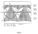
- FIG 3 shows the course of the voltage U P at the point P and the course of the current I L2a , wherein the zero line of the voltage U P and the current I L2a by the arrow for the channels 1, 3 on the left side of the diagram of FIG 3 is marked.
- the energy from the boost converter inductor L2a is discharged into the parasitic capacitances (left half of FIG. 3).
- the inductor L2a is now magnetized in the opposite direction.
- the negative rash, see the course of the current I L2a almost reaches the level of the previous positive maximum.
- the current I L2a is almost mean free. As a result, hardly any power is taken from the network.
- the invention is based on the recognition that this reversal of the current I L2a by the boost converter inductor L2a can be reduced if a decoupling diode is arranged in series with the boost converter switch T1. This reduces the negative precharge of the boost converter inductor L2a and thus improves the waveform of the grid current IN.
- a preferred embodiment is characterized in that the decoupling diode between the connection point P, via which the boost converter inductor is coupled to the boost converter diode, and the boost converter switch is coupled.
- An alternative to this is characterized in that the decoupling diode is coupled between the boost converter switch and a reference potential. In the latter embodiment, a shunt for current detection may be coupled between the decoupling diode and the reference potential.
- the already mentioned control device can be designed to control the boost converter switch in such a way that its switch-on time in stationary operation is fixed independently of the instantaneous voltage and the pause time is variable.
- the circuit arrangement comprises a device for detecting the change in direction of the current through the boost converter inductor, wherein the control device is designed to control the pause time in dependence on the change in direction of the current through the boost converter inductor.
- the control device is preferably designed to switch on the boost converter switch when the detected instantaneous value of the current through the boost converter throttle is equal to zero.
- FIG. 4 shows an exemplary embodiment of a circuit arrangement according to the invention, wherein the reference numbers introduced with reference to FIG. 1 for identical and identically acting elements have been adopted and will not be described again.
- the embodiment of the circuit arrangement illustrated in FIG. 4 differs from the circuit arrangement illustrated in FIG. 1 in that a decoupling diode D6 is inserted in series with the step-up converter switch T1.
- this is inserted between the point P and the boost converter switch T1.
- a decoupling diode could be inserted between the boost converter switch T1 and the reference potential.
Landscapes
- Engineering & Computer Science (AREA)
- Physics & Mathematics (AREA)
- Electromagnetism (AREA)
- General Physics & Mathematics (AREA)
- Radar, Positioning & Navigation (AREA)
- Automation & Control Theory (AREA)
- Dc-Dc Converters (AREA)
Priority Applications (1)
| Application Number | Priority Date | Filing Date | Title |
|---|---|---|---|
| EP06008130A EP1848099A1 (fr) | 2006-04-19 | 2006-04-19 | Ensemble de circuit et procédé pour le fonctionnement d' au moins une charge |
Applications Claiming Priority (1)
| Application Number | Priority Date | Filing Date | Title |
|---|---|---|---|
| EP06008130A EP1848099A1 (fr) | 2006-04-19 | 2006-04-19 | Ensemble de circuit et procédé pour le fonctionnement d' au moins une charge |
Publications (1)
| Publication Number | Publication Date |
|---|---|
| EP1848099A1 true EP1848099A1 (fr) | 2007-10-24 |
Family
ID=37403143
Family Applications (1)
| Application Number | Title | Priority Date | Filing Date |
|---|---|---|---|
| EP06008130A Withdrawn EP1848099A1 (fr) | 2006-04-19 | 2006-04-19 | Ensemble de circuit et procédé pour le fonctionnement d' au moins une charge |
Country Status (1)
| Country | Link |
|---|---|
| EP (1) | EP1848099A1 (fr) |
Citations (2)
| Publication number | Priority date | Publication date | Assignee | Title |
|---|---|---|---|---|
| EP0507393A2 (fr) * | 1991-04-04 | 1992-10-07 | Koninklijke Philips Electronics N.V. | Agencement de circuit |
| US5650925A (en) * | 1995-02-09 | 1997-07-22 | Magnetek, Inc. | Diode clamping arrangement for use in electronic ballasts |
-
2006
- 2006-04-19 EP EP06008130A patent/EP1848099A1/fr not_active Withdrawn
Patent Citations (2)
| Publication number | Priority date | Publication date | Assignee | Title |
|---|---|---|---|---|
| EP0507393A2 (fr) * | 1991-04-04 | 1992-10-07 | Koninklijke Philips Electronics N.V. | Agencement de circuit |
| US5650925A (en) * | 1995-02-09 | 1997-07-22 | Magnetek, Inc. | Diode clamping arrangement for use in electronic ballasts |
Similar Documents
| Publication | Publication Date | Title |
|---|---|---|
| DE102004033354B4 (de) | Verfahren zur Ansteuerung eines Schalters in einem Hochsetzsteller und Ansteuerschaltung | |
| DE69623394T2 (de) | Schaltkreis und Verfahren zum Steuerung eines Einschaltstrombegrenzers in ein Leistungswandler mit Leistungsfaktorkorrektur | |
| DE19909464C2 (de) | Verfahren zur Erzeugung einer geregelten Gleichspannung aus einer Wechselspannung und Stromversorgungseinrichtung zur Durchführung des Verfahrens | |
| DE112014004225T5 (de) | Ladungspumpenzeitsteuerung | |
| DE102015105488A1 (de) | System und verfahren für eine getaktete leistungsversorgung | |
| EP1892811A2 (fr) | Circuit convertisseur de puissance et procédé d'alimentation de réseau à partir d'une source de tension continue non constant | |
| DE102015112245B4 (de) | Gleichrichter | |
| EP3114898B1 (fr) | Led-driver | |
| DE102017222265A1 (de) | Gleichspannungswandler | |
| EP0637118B1 (fr) | Circuit pour limiter le courant de démarrage et surtension d'un ballast électronique | |
| DE102009042419B4 (de) | Schaltungsanordnung zum Betreiben mindestens einer LED | |
| DE102016220204A1 (de) | Verfahren zum Betreiben eines Gleichspannungswandlers, Steuervorrichtung für einen Gleichspannungswandler und Gleichspannungswandler | |
| EP2951912B1 (fr) | Procédé de réglage d'un onduleur et onduleur | |
| EP1848099A1 (fr) | Ensemble de circuit et procédé pour le fonctionnement d' au moins une charge | |
| DE102012005854A1 (de) | Elektrische Versorgungsvorrichtung | |
| WO2001089070A1 (fr) | Dispositif pour maintenir une tension d'alimentation | |
| WO2000079675A1 (fr) | Procede d'identification d'une charge connectable a la demande a un onduleur et systeme d'identification de charge correspondant | |
| LU101923B1 (de) | Aufwärtswandler für eine Stromversorgung eines elektrischen Verbrauchers sowie Stromversorgung und Verfahren zur Aufwärtswandlung der Eingangsspannung in einer Stromversorgung eines elektrischen Verbrauchers | |
| DE19505417A1 (de) | Schaltnetzteil, insbesondere PFC-bewerteter Tief-/Hochsetzsteller | |
| DE10307823B4 (de) | Schaltungsanordnung zur Lüfterregelung | |
| DE102009039770B4 (de) | Verfahren und Vorrichtung zum Betrieb eines Spannungszwischenkreis-Umrichters bei Transienten im speisenden Netz | |
| DE102008034989B4 (de) | Schaltungsanordnung und Verfahren zur Steuerung der Leistungsaufnahme von Beleuchtungsanlagen mit Wechselspannungsspeisung | |
| EP4200965A1 (fr) | Procédé de fonctionnement d'une unité d'alimentation électrique à découpage et dispositif d'alimentation en tension | |
| AT405228B (de) | Netzgleichrichterschaltung | |
| DE102004046283A1 (de) | Verfahren und Vorrichtung zum Versorgen von Wechselspannungsverbrauchern mit variabler Leistung |
Legal Events
| Date | Code | Title | Description |
|---|---|---|---|
| PUAI | Public reference made under article 153(3) epc to a published international application that has entered the european phase |
Free format text: ORIGINAL CODE: 0009012 |
|
| AK | Designated contracting states |
Kind code of ref document: A1 Designated state(s): AT BE BG CH CY CZ DE DK EE ES FI FR GB GR HU IE IS IT LI LT LU LV MC NL PL PT RO SE SI SK TR |
|
| AX | Request for extension of the european patent |
Extension state: AL BA HR MK YU |
|
| AKX | Designation fees paid | ||
| STAA | Information on the status of an ep patent application or granted ep patent |
Free format text: STATUS: THE APPLICATION IS DEEMED TO BE WITHDRAWN |
|
| 18D | Application deemed to be withdrawn |
Effective date: 20080425 |
|
| REG | Reference to a national code |
Ref country code: DE Ref legal event code: 8566 |