EP3114898B1 - Led-driver - Google Patents
Led-driver Download PDFInfo
- Publication number
- EP3114898B1 EP3114898B1 EP15702500.8A EP15702500A EP3114898B1 EP 3114898 B1 EP3114898 B1 EP 3114898B1 EP 15702500 A EP15702500 A EP 15702500A EP 3114898 B1 EP3114898 B1 EP 3114898B1
- Authority
- EP
- European Patent Office
- Prior art keywords
- switch
- output voltage
- vout
- voltage
- tdischarge
- Prior art date
- Legal status (The legal status is an assumption and is not a legal conclusion. Google has not performed a legal analysis and makes no representation as to the accuracy of the status listed.)
- Active
Links
Images

Classifications
-
- H—ELECTRICITY
- H02—GENERATION; CONVERSION OR DISTRIBUTION OF ELECTRIC POWER
- H02M—APPARATUS FOR CONVERSION BETWEEN AC AND AC, BETWEEN AC AND DC, OR BETWEEN DC AND DC, AND FOR USE WITH MAINS OR SIMILAR POWER SUPPLY SYSTEMS; CONVERSION OF DC OR AC INPUT POWER INTO SURGE OUTPUT POWER; CONTROL OR REGULATION THEREOF
- H02M3/00—Conversion of DC power input into DC power output
- H02M3/22—Conversion of DC power input into DC power output with intermediate conversion into AC
- H02M3/24—Conversion of DC power input into DC power output with intermediate conversion into AC by static converters
- H02M3/28—Conversion of DC power input into DC power output with intermediate conversion into AC by static converters using discharge tubes with control electrode or semiconductor devices with control electrode to produce the intermediate AC
- H02M3/325—Conversion of DC power input into DC power output with intermediate conversion into AC by static converters using discharge tubes with control electrode or semiconductor devices with control electrode to produce the intermediate AC using devices of a triode or a transistor type requiring continuous application of a control signal
- H02M3/335—Conversion of DC power input into DC power output with intermediate conversion into AC by static converters using discharge tubes with control electrode or semiconductor devices with control electrode to produce the intermediate AC using devices of a triode or a transistor type requiring continuous application of a control signal using semiconductor devices only
- H02M3/33507—Conversion of DC power input into DC power output with intermediate conversion into AC by static converters using discharge tubes with control electrode or semiconductor devices with control electrode to produce the intermediate AC using devices of a triode or a transistor type requiring continuous application of a control signal using semiconductor devices only with automatic control of the output voltage or current, e.g. flyback converters
- H02M3/33523—Conversion of DC power input into DC power output with intermediate conversion into AC by static converters using discharge tubes with control electrode or semiconductor devices with control electrode to produce the intermediate AC using devices of a triode or a transistor type requiring continuous application of a control signal using semiconductor devices only with automatic control of the output voltage or current, e.g. flyback converters with galvanic isolation between input and output of both the power stage and the feedback loop
-
- H—ELECTRICITY
- H05—ELECTRIC TECHNIQUES NOT OTHERWISE PROVIDED FOR
- H05B—ELECTRIC HEATING; ELECTRIC LIGHT SOURCES NOT OTHERWISE PROVIDED FOR; CIRCUIT ARRANGEMENTS FOR ELECTRIC LIGHT SOURCES, IN GENERAL
- H05B45/00—Circuit arrangements for operating light-emitting diodes [LED]
- H05B45/30—Driver circuits
- H05B45/37—Converter circuits
- H05B45/3725—Switched mode power supply [SMPS]
- H05B45/382—Switched mode power supply [SMPS] with galvanic isolation between input and output
-
- H—ELECTRICITY
- H05—ELECTRIC TECHNIQUES NOT OTHERWISE PROVIDED FOR
- H05B—ELECTRIC HEATING; ELECTRIC LIGHT SOURCES NOT OTHERWISE PROVIDED FOR; CIRCUIT ARRANGEMENTS FOR ELECTRIC LIGHT SOURCES, IN GENERAL
- H05B45/00—Circuit arrangements for operating light-emitting diodes [LED]
- H05B45/30—Driver circuits
- H05B45/37—Converter circuits
- H05B45/3725—Switched mode power supply [SMPS]
- H05B45/385—Switched mode power supply [SMPS] using flyback topology
Definitions
- the invention relates to an operating device for controlling lighting means such. LED routes, as well as a control unit for controlling such a control gear.
- the invention also relates to a method for controlling lighting means, such as e.g. LED routes.
- flyback converter it is known to use a flyback converter to operate an LED module.
- the flyback converter is part of a corresponding operating device and is used e.g. operated in Critical Conduction mode, also called Borderline mode.
- Critical Conduction mode also called Borderline mode.
- the switch of the flyback converter is switched on the primary side, so that in this switch-on phase, the primary-side current increases constantly. This causes a constant negative voltage on a detection winding on the flyback converter.
- the switch When the current has reached a predetermined peak value, the switch is turned off. After switching off, the voltage on the detection winding jumps to a positive value, oscillates for a certain period of time and then settles to a voltage value corresponding to the output voltage Vout.
- the secondary side current decreases linearly during this shutdown phase.
- the steady and preferably linear voltage on the detection winding decreases.
- the voltage at the detection winding thus buckles.
- Critical Conduction mode it is now necessary to use the To be able to detect zero point of the secondary-side current, and then turn on the switch of the flyback converter again.
- this switch-on threshold can more accurately detect the kinking of the detection voltage by sampling the steady-state voltage when the switch is switched off, and depending on this, ie, the switch-off threshold is selected as a function of the sampled voltage.
- the steady-state voltage which thus corresponds to the output voltage of the flyback converter, depends on the specific configuration of the LED module, in particular on the number of LEDs in the LED module.
- an operating device according to claim 1 is provided.
- Advantageous embodiments of the operating device according to the invention are defined by the dependent claims.
- a method according to claim 8 is also provided.
- An advantageous embodiment of the method according to the invention is defined by the dependent claim.
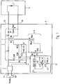
- the operating device 1 preferably has an input stage 2, a converter 3, a detection unit 4 and a control unit ST.
- the input stage 2 is optional and can be used to filter the mains supply voltage Vmains.
- the input stage 2 filter components or circuits (not shown).
- the input stage 2 can rectify the optionally filtered mains supply voltage Vmains, e.g. by a full-bridge rectifier with four diodes for converting the AC voltage into a pulsating DC voltage.
- the output of the optional input stage 2 is the voltage Vin and is supplied to the converter 3.
- This voltage Vin is preferably a rectified AC voltage, in particular a half-wave rectified AC voltage.
- the converter 3 is formed in the illustrated embodiment by a so-called flyback converter, which can also be referred to as flyback converter or high-buck converter.
- the converter 3 is a voltage converter or DC-DC converter and may also have alternative topologies, in particular topologies comprising a galvanic isolation.
- the flyback converter is in the embodiment of Fig. 1 that is, as an example of a clocked by at least one switch M1 electrically isolated converter, which may have a transformer for potential separation.
- the operating device 1 instead other clocked circuits, in particular with galvanic Have separation, such as a forward converter, also called forward converter, or a push-pull converter, also called push-pull converter, such as a push-pull converter with half-bridge or full bridge drive.
- the flyback converter 3 has a transformer T in the form of, for example, a transformer with a primary winding N1 and a secondary winding N2.
- the transformer T is used for potential separation between a primary side and a secondary side.
- the transformer T serves to transmit electrical energy from the primary winding N1 to the secondary winding N2 or from the primary side to the secondary side.
- the energy is preferably taken up in two different phases on the primary side and discharged again on the secondary side.
- a transformer in the form of a transformer therefore preferably has an air gap for temporarily storing the energy between the two phases.
- the flyback converter 3 comprises a controllable switch M1.
- a controllable switch M1 In a known manner can be transmitted to the secondary side of the flyback converter 3 by a corresponding alternately opening and closing the switch M1, the voltage applied from the input side to the flyback converter voltage Vin available. This transferred to the secondary side energy can be used to operate the secondary side connectable LED module 5. The energy transfer takes place in the open state of the switch M1, wherein for this purpose on the output side of the flyback converter 3, a diode D1 is further provided.
- the switch M1 is connected in series with the primary winding N1, so that by closing the controllable switch M1, a primary-side current can flow through this primary winding N1. When switch S1 is open, however, no current can flow through this primary winding N1.
- the switch M1 is designed, for example, as a controllable transistor, in particular as a FET or MOSFET transistor.
- the switch M1 is controlled by the control unit ST of the operating device.
- this control unit ST is located on the primary side of the flyback converter or the transformer T.
- the switch M1 is a MOSFET transistor, wherein the gate input of the switch M1 is designed as a control input and is connected to the control unit ST.
- the switch M1 is turned on and off via the control input by a control signal S / M1 generated by the control unit ST.
- the switch M1 of Fig. 1 is designed in particular as a p-channel, wherein the drain terminal is connected to a terminal of the primary winding N1.
- the source terminal of the switch M1 is preferably coupled to ground, ie to the primary side ground.
- the flyback converter 3 On the input side, the flyback converter 3 has a capacitor C_bulk, to which the input voltage Vin of the flyback converter 3 is applied.
- the diode D1 provided on the secondary side is connected in series with the secondary winding N2. Parallel to the series connection of the diode D1 and the secondary winding N2, a capacitor Cout is provided. The voltage across this capacitor Cout forms the output voltage Vout of the flyback converter 3, which in turn connects to two Output terminals K3, K4 is provided.
- the LED module 5 can be connected to these output terminals K3, K4.
- the LED module 5 has one or more LEDs, preferably an LED track comprising a plurality of LEDs connected in series.
- the LED module 5 may also comprise a parallel circuit of a plurality of LED paths or a mixed circuit of parallel and serially connected LEDs.
- a measuring resistor R1 can be provided between the switch M1 and ground. At this measuring resistor R1, a signal can be tapped, this signal VR1 the current 11 through the primary winding M1 reproduces. This measured signal is compared by a comparator Kp with a reference signal or with a reference voltage Vref_hi0. The output of the comparator Kp is fed to the control unit ST, as an alternative to the embodiment of the Fig. 1 the comparator Kp and the reference voltage Vref_hi0 may also be provided internally in the control unit ST.
- a maximum value I1max is provided for the primary-side current I1.
- This maximum value I1max can be externally supplied to the operating device 1, or can be determined by the operating device.
- the reference voltage Vref_hi0 is now preferably set so that when the primary-side current I1 reaches this maximum value I1max, then the measured signal VR1 corresponds to the reference Vref_hi0.
- the output of the comparator Kp thus provides the operating device 1 with information as to whether the primary-side current I1 is below the maximum value I1max or whether the primary-side current I1 has reached the maximum value I1max.
- the operating device 1 is thus able to switch M1 open as soon as the primary-side current I1 reaches the maximum value I1max or as soon as the measured signal VR1 reaches or exceeds the reference Vref_hi0.
- the typical time profile of the voltage VR1 representative of the current I1 is in Fig. 2 shown.
- the controllable switch M1 is controlled by the control unit ST of the operating device, preferably without electrical isolation between the switch M1 and the control unit ST.
- the transformer or the transformer T comprises in addition to the primary winding N1 and the secondary winding N2 nor an auxiliary winding or detection winding Naux, which is preferably located on the primary side of the transformer T.
- auxiliary winding Naux On the auxiliary winding Naux is a voltage Vaux, which reproduces the output voltage Vout.
- Vaux K1 * Vout, where K1 is a constant that depends on the winding ratios of the secondary winding and the auxiliary winding.
- an ohmic voltage divider consisting of two resistors R2, R3 is provided, at which a detection signal or a detection voltage VR3 for detecting the voltage Vaux at the auxiliary winding Naux is tapped.
- This tension VR3 is also representative of the output voltage Vout and proportional to the latter.
- the detection signal VR3 is supplied to the control unit ST.
- the detection winding Naux and the voltage divider R2, R3 together form the detection unit 4.
- the switch M1 When the switch M1 is switched on on the primary side, the current I1 rises constantly on the primary side, which induces a constant negative voltage Vaux in the detection unit 4. When the current I1 has reached the predetermined maximum value I1max, the power switch M1 is turned off. Thereafter, the detection voltage Vaux jumps to a positive value, oscillates for a certain period of time and then settles to a voltage value corresponding to the output voltage Vout.
- the detection voltage VR3 is preferably supplied to a first comparator K1 and a second comparator K2.
- the detection signal VR3 is compared with a first reference voltage Vref_lo.
- This reference voltage Vref_lo is preferably a switch-on threshold for switching on or switching back on the controllable switch M1.
- the switch M1 is turned on again on the primary side.
- this threshold Vref_lo is reached at time t4.
- the control signal S / M1 for switching on the switch M1 is then preferably increased, for example, from zero to a positive value.
- the switch M1 can be closed by the control unit ST as soon as the voltage at the auxiliary winding Naux reaches a corresponding lower threshold value. Since the detection voltage VR3 is representative of both the voltage Vaux on the auxiliary winding and the output voltage Vout, therefore, the switch M1 is closed again as soon as the output voltage Vout has reached a corresponding lower threshold value.
- the reference voltage Vref_lo is preferably a fixed comparator threshold, which can be preset, for example.
- the reference voltage Vref_lo can for example be predefined in the operating device 1, or it can be preset externally via a corresponding interface of the operating device 1. After the specification of a certain value Vref_lo, this reference voltage preferably remains constant. At least the reference Vref_lo remains constant for the duration of several switching cycles of the switch M1. In particular, the reference Vref_lo is independent of feedback values or measured values from the range of the operating device 1 or the LED module 5.
- the reference voltage Vref_lo is preferably less than half, in particular less than 20%, 10% or 5% of the detection voltage VR3 in the steady state after opening the switch M1.
- the flyback converter 3 can be operated according to a continuous current mode (current continuous conduction mode), a discontinuous current mode (discontinuous current mode), or according to an operation in the boundary region between continuous and discontinuous current current operation.
- the operating device 1 according to the invention is operated in this boundary region, which is also called critical conduction mode or borderline mode.
- critical conduction mode the switch M1 of the flyback converter 3 is turned on as soon as it is detected that the current through the secondary winding N2 has dropped to zero.
- the switch M1 is turned on when the detection voltage VR3 reaches or falls below the lower reference voltage Vref_lo.
- the current I2 through the secondary winding N2 is a measure of the current through the LEDs or through the LED module 5.
- the mean value of the current I2 corresponds to the mean value of the current through the LEDs.
- the second comparator K2 is now used in particular for accurately detecting the discharge time Tdischarge the secondary winding N2 between turning off the switch M1 and reaching the zero point by the secondary side current I2, wherein at the zero crossing of the current I2, the voltage Vaux on the auxiliary winding Naux or the detection voltage VR3 kinks.
- the second comparator K2 compares the detection voltage VR3 with a variable reference voltage in the form of an adaptive threshold Vref_hi.
- the sense voltage is also applied to a sample-and-hold circuit S + H, the latter being able to briefly hold the analog values of the sense voltage.
- This sample-and-hold circuit S + H is used in particular to sample the steady-state when the switch is turned off.
- the output of the sample-and-hold circuit is fed to an analog-to-digital converter ADC for converting the analog values into digital values.
- the adaptive threshold value Vref_hi is preferably dependent on the value of the output voltage Vout in the steady state state determined by the sample-and-hold circuit S + H and the analog-to-digital converter ADC. This dependence is in Fig. 1 represented by the arrow 8.
- an adaptive restart threshold Vref_hi is selected.
- the adaptive switch-on threshold Vref_hi may be selected as a certain percentage below the steady-state voltage, eg, 95%, 90%, or 80% of the value of the steady-state voltage VR3.
- This reference voltage Vref_lo is in particular smaller than the adaptive threshold value Vref_hi.
- the reference voltage Vref_lo is also preferably a non-variable value. Turning the switch M1 back on depending on the first comparator K1 is advantageous in that e.g. when the low reference voltage Vref_lo is reached, the mains voltage Vmains is also low, so that the losses in the switch M1 can be kept low.
- the undershooting of the adaptive, and thus higher selected, reclosing threshold Vref_hi is thus preferably taken only for more accurate determination of the discharge period Tdischarge for the indirect determination of the secondary-side current I2.
- the actual reconnection of the primary-side switch preferably takes place only when, in the further course of the decay of the detection voltage VR3, the threshold value Vref_lo, which is still fixed, is undershot.
- Fig. 2 shows the course of different sizes of the operating device 1 over a period Tperiod of the flyback converter 3, ie during the period of a complete switching cycle of the switch consisting of a switch-on time Ton of the switch M1 and a subsequent turn-off time Toff of the switch M1.
- Tperiod of the flyback converter 3 ie during the period of a complete switching cycle of the switch consisting of a switch-on time Ton of the switch M1 and a subsequent turn-off time Toff of the switch M1.
- Tperiod of the flyback converter 3 ie during the period of a complete switching cycle of the switch consisting of a switch-on time Ton of the switch M1 and a subsequent turn-off time Toff of the switch M1.
- the control unit ST generates the control signal S / M1 for driving the switch M1.
- the switch M1 is closed by the control unit ST by means of the control signal S / M1.
- the control signal S / M1 causes the opening of the switch M1 during a turn-off period toff.
- the switch M1 is alternately turned on and off, so that in operation after the in Fig. 2 turn off time toff again a turn-on time ton occurs.
- the switch-on time duration t on and the following switch-off time duration t off together form a period Tperiod of the operating device 1 or of the flyback converter 3. In operation, this results in a sequence of several periods Tperiod.
- the primary-side current I1 through the primary winding N1 and through the switch M1 is reproduced from the measuring voltage VR1, this measurement being picked up at the measuring resistor R1.
- a current flows through the primary winding N1.
- This primary-side current I1 rises linearly from a zero value.
- the measured signal VR1 also increases during the on-time period ton as in Fig. 2 shown.
- the control unit ST causes the switch M1 to be opened. Consequently, the diode D1 is operated in the forward direction and in the transformer energy stored during the turn-on period ton is transmitted to the secondary side of the transformer T. At time t1, therefore, the secondary-side current I2 through the diode D1 increases to a positive value and begins to decrease linearly again.
- Fig. 2 also shows the course of the voltage Vaux and the auxiliary winding Naux and the measured voltage VR3, these voltages are proportional to each other.
- the detected voltage has a constant negative value.
- the detection voltage jumps to a positive value, oscillates for a certain period of time and then settles to a voltage value corresponding to the output voltage Vout.
- the steady-state oscillation voltage after oscillation can remain constant or have a constant negative slope.
- this steady-state detection voltage has a kinking.
- this kinking occurs when the current I2 drops to zero through the secondary winding N2.
- the detection voltage Vaux oscillates the detection voltage Vaux, in which it preferably alternately drops to zero and rises again.
- the threshold value Vref_hi for detecting the discharge period Tdischarge is preferably dependent on the value of the settled detection voltage VR3.
- a waiting time WT can be stored in the control unit ST.
- This waiting time WT is in Fig. 2 represents and defines the period of time after Switching off the switch M1 must be awaited before the detection voltage VR3 is detected or sampled to determine the threshold value Vref_hi.
- the waiting time WT which must be met after switching off the switch to be sure that the output voltage or the detection voltage VR3 has settled, can be fixed as already seen.
- this waiting time WT can be fixed only at the beginning of the LED operation.
- this wait time WT can be adaptively redefined.
- the waiting time of a particular cycle may be a certain percentage of the discharge duration Tdischarge of the previous cycle.
- Fig. 2 shows, for example, that at the beginning of the LED operation, the output voltage or the detection voltage VR3 is detected after the predetermined waiting time WT.
- a waiting time WT ' is waited, this waiting time WT' being, for example, x% of the unloading time Tdischarge, eg 90% or 80%.
- correction factor .DELTA.T which depends on the sampled reference voltage VR3 is then determined as a correction factor.
- These correction values .DELTA.T can be empirical values, for example, which can be stored in a memory or in a look-up table within the control unit ST. The correspondence between the sampled reference voltage VR3 and the consequent correction value ⁇ T is stored in this memory or in this look-up table.
- the common denominator of these embodiments is therefore that the discharge period Tdischarge is preferably determined taking into account the detection of the detection voltage or the output voltage in the steady state.
- the comparator can be eliminated.
- the kinking of the detection voltage VR3 at the time t3 after the stationary state can be detected directly with a fast analog-to-digital converter.
- Comparator K2 is not needed and replaced by an analog-to-digital converter (not shown).
- the control unit ST checks the digital data generated by this analog-to-digital converter. As soon as the detection voltage VR3 is in the steady state, the control unit ST detects a possible bending of the detection voltage VR3 on the basis of this digital data. The detected time of the kinking is then determined by the control unit ST as the zero crossing of the current I2. Based on the time duration between the switching off of the switch M1 and the bending of the detection voltage, the control unit ST can finally determine the secondary current, as explained above.
- the output voltage Vout is detected indirectly, namely as the voltage which is stationary at the auxiliary winding Naux in the switched off switch state.
- a more direct detection of the output voltage can also be provided, in particular via the detection of a secondary-side parameter, for example via the detection of the output voltage Vout, and then transmission via the galvanic isolation, for example by means of optocouplers.
- the common denominator of the invention is therefore that the output voltage Vout is detected directly or indirectly, on the primary side or on the secondary side, and is included in the calculation of the discharge period Tdischarge as a variable.
Landscapes
- Engineering & Computer Science (AREA)
- Power Engineering (AREA)
- Dc-Dc Converters (AREA)
- Circuit Arrangement For Electric Light Sources In General (AREA)
- Led Devices (AREA)
Claims (9)
- Appareil de commande (1) pour la commande de moyens d'éclairage, comprenant :- un convertisseur cadencé à potentiel séparé (3) avec un transmetteur (T) comprenant un enroulement primaire (N1) et un enroulement secondaire (N2) et un commutateur contrôlable (M1) disposé côté primaire, le convertisseur (3) pouvant être alimenté côté primaire avec une tension d'alimentation et les moyens d'éclairage peuvent être alimentés côté secondaire par l'intermédiaire d'une tension de sortie (Vout) du convertisseur (3),- des moyens (4) pour la mesure directe ou indirecte de la tension de sortie (Vout) et- une unité de commande (ST) pour le contrôle du commutateur (M1),moyennant quoi, lorsque le commutateur (M1) est désactivé, le courant du secondaire (I2) à travers l'enroulement secondaire (N2) chute de manière linéaire à partir d'une valeur positive (I2max),
l'unité de commande (ST) étant conçue, pour la régulation du courant secondaire (I2), pour mesurer une durée de décharge (Tdischarge) entre une désactivation du commutateur (M1) et une chute suivante du courant secondaire (I2) à zéro,
caractérisé en ce que
l'unité de commande (ST) est conçue pour déterminer la durée de décharge (Tdischarge) en fonction d'une comparaison d'une tension de sortie mesurée avec une valeur seuil adaptative (Vref_hi). - Appareil de commande selon la revendication 1,
la durée de décharge (Tdischarge) étant déterminée en tenant compte de la mesure d'une tension de sortie (Vout) appliquée après la désactivation du commutateur (M1). - Appareil de commande selon la revendication 1,
la valeur seuil adaptative (Vref_hi) dépendant d'une valeur de la tension de sortie (Vout) appliquée après la désactivation du commutateur (M1). - Appareil de commande selon la revendication 3,
l'unité de commande (ST) étant conçue pour sélectionner la valeur seuil (Vref_hi) en tant que pourcentage déterminé en dessous de la valeur de la tension de sortie (Vout) appliquée après la désactivation du commutateur (M1). - Appareil de commande selon la revendication 1 ou 2,
moyennant quoi, pour la mesure de la durée de décharge (Tdischarge), un moment (t4) du passage en dessous d'une valeur seuil fixe (Vref_lo) est d'abord déterminé par la tension de sortie (Vout) mesurée puis ce moment (t4) est corrigé par une durée adaptative (ΔT). - Appareil de commande selon la revendication 5,
la durée adaptative (ΔT) dépendant d'une valeur mesurée de la tension de sortie (Vout) appliquée après la désactivation du commutateur (M1). - Appareil de commande (1) selon la revendication 1, comprenant :un convertisseur analogique-numérique pour la conversion de la tension de sortie analogique (Vout) mesurée en valeurs numériques,l'unité de commande (ST) étant conçue, pour la régulation du courant secondaire (I2), pour mesurer une durée de décharge (Tdischarge) entre une désactivation du commutateur (M1) et une chute suivante du courant secondaire (I2) à zéro en fonction des valeurs numériques.
- Procédé de commande de moyens d'éclairage
à l'aide d'un convertisseur cadencé à potentiel séparé (3) avec un transmetteur (T) comprenant un enroulement primaire (N1) et un enroulement secondaire (N2) et un commutateur contrôlable (M1) disposé côté primaire,
moyennant quoi, lorsque le commutateur (M1) est désactivé, le courant secondaire (I2) à travers l'enroulement secondaire (N2) chute de manière linéaire à partir d'une valeur positive (I2max),
le convertisseur (3) étant alimenté côté primaire avec une tension d'alimentation et les moyens d'éclairage étant alimentés côté secondaire par l'intermédiaire d'une tension de sortie (Vout) du convertisseur (3),
moyennant quoi, pour la régulation du courant secondaire (I2), une durée de décharge (Tdischarge) entre une désactivation du commutateur (M1) et une chute suivante du courant secondaire (I2) à zéro est mesurée,
caractérisé en ce que
la durée de décharge (Tdischarge) est déterminée en fonction d'une comparaison d'une tension de sortie (Vout) mesurée avec une valeur seuil adaptative (Vref_hi). - Procédé selon la revendication 8,
la tension de sortie (Vout) étant mesurée directement ou indirectement et converti en valeurs numériques et
pour la régulation du courant secondaire (I2), la durée de décharge (Tdischarge) entre une désactivation du commutateur (M1) et une chute suivante du courant secondaire (12) à zéro est mesurée en fonction des valeurs numériques.
Applications Claiming Priority (2)
| Application Number | Priority Date | Filing Date | Title |
|---|---|---|---|
| DE102014204127.9A DE102014204127A1 (de) | 2014-03-06 | 2014-03-06 | LED-Treiber |
| PCT/EP2015/052381 WO2015132032A2 (fr) | 2014-03-06 | 2015-02-05 | Led-treiber |
Publications (2)
| Publication Number | Publication Date |
|---|---|
| EP3114898A2 EP3114898A2 (fr) | 2017-01-11 |
| EP3114898B1 true EP3114898B1 (fr) | 2018-12-05 |
Family
ID=52446378
Family Applications (1)
| Application Number | Title | Priority Date | Filing Date |
|---|---|---|---|
| EP15702500.8A Active EP3114898B1 (fr) | 2014-03-06 | 2015-02-05 | Led-driver |
Country Status (5)
| Country | Link |
|---|---|
| US (1) | US10172195B2 (fr) |
| EP (1) | EP3114898B1 (fr) |
| CN (1) | CN106105394B (fr) |
| DE (1) | DE102014204127A1 (fr) |
| WO (1) | WO2015132032A2 (fr) |
Families Citing this family (8)
| Publication number | Priority date | Publication date | Assignee | Title |
|---|---|---|---|---|
| DE102015210710A1 (de) * | 2015-06-11 | 2016-12-15 | Tridonic Gmbh & Co Kg | Getaktete Sperrwandlerschaltung |
| DE102016222161A1 (de) * | 2016-11-11 | 2018-05-17 | Tridonic Gmbh & Co Kg | Sperrwandler zum Betreiben von einem oder mehreren Leuchtmitteln, dazugehöriges Verfahren und Betriebsgerät |
| CN108880274A (zh) * | 2017-05-15 | 2018-11-23 | 赤多尼科两合股份有限公司 | 一种谐振变换器的输出电流检测电路 |
| TWI629917B (zh) * | 2017-07-26 | 2018-07-11 | 大樑科技實業有限公司 | 照明系統 |
| CN108599108B (zh) * | 2018-04-30 | 2023-11-17 | 上海晶丰明源半导体股份有限公司 | 保护电路、驱动系统、芯片及电路保护方法、驱动方法 |
| EP3890445B1 (fr) * | 2020-03-31 | 2025-12-10 | Tridonic GmbH & Co. KG | Convertisseur à commutation côté primaire pour fournir une tension d'alimentation à une charge de del |
| EP4054066A1 (fr) * | 2021-03-02 | 2022-09-07 | Tridonic GmbH & Co. KG | Convertisseur indirect synchrone |
| DE102021113015B4 (de) | 2021-05-19 | 2023-07-27 | Steinel Gmbh | Schaltungsanordnung für ein Flyback-Netzteil zum Betrieb und zur Erfassung einer Temperatur zumindest einer LED |
Citations (2)
| Publication number | Priority date | Publication date | Assignee | Title |
|---|---|---|---|---|
| US20040052095A1 (en) * | 2001-11-29 | 2004-03-18 | Iwatt, Inc | Methods for digital regulation of power converters using primary-only feedback |
| EP2645819A1 (fr) * | 2012-03-30 | 2013-10-02 | Samsung Electro-Mechanics Co., Ltd | Appareil de commande de diode électroluminescente |
Family Cites Families (11)
| Publication number | Priority date | Publication date | Assignee | Title |
|---|---|---|---|---|
| DE19828038A1 (de) * | 1998-06-24 | 1999-12-30 | Philips Corp Intellectual Pty | Schaltnetzteil |
| US7016204B2 (en) | 2004-08-12 | 2006-03-21 | System General Corp. | Close-loop PWM controller for primary-side controlled power converters |
| JP4373995B2 (ja) * | 2005-06-24 | 2009-11-25 | フリボ モバイル パワー ゲーエムベーハー | スイッチモード電源における電流および電圧を制御するための制御回路 |
| EP2110938B1 (fr) * | 2008-04-14 | 2018-08-29 | Power Systems Technologies GmbH | Circuit de commande primaire pour un convertisseur électronique de puissance comportant un transformateur sans enroulement auxiliaire avec un réglage basé sur la durée de continuité de courant du côté secondaire |
| US9173261B2 (en) | 2010-07-30 | 2015-10-27 | Wesley L. Mokry | Secondary-side alternating energy transfer control with inverted reference and LED-derived power supply |
| US8912781B2 (en) | 2010-07-30 | 2014-12-16 | Cirrus Logic, Inc. | Integrated circuit switching power supply controller with selectable buck mode operation |
| CN102340911B (zh) | 2010-12-30 | 2013-08-07 | 矽力杰半导体技术(杭州)有限公司 | 一种led驱动器的控制电路及其控制方法 |
| US9313840B2 (en) | 2011-06-03 | 2016-04-12 | Cirrus Logic, Inc. | Control data determination from primary-side sensing of a secondary-side voltage in a switching power converter |
| KR20140017305A (ko) | 2012-07-31 | 2014-02-11 | 삼성전기주식회사 | 발광 다이오드 구동 장치 |
| CN103066872B (zh) * | 2013-01-17 | 2015-06-17 | 矽力杰半导体技术(杭州)有限公司 | 一种集成开关电源控制器以及应用其的开关电源 |
| AT14906U1 (de) * | 2013-11-28 | 2016-08-15 | Tridonic Gmbh & Co Kg | LED-Modul |
-
2014
- 2014-03-06 DE DE102014204127.9A patent/DE102014204127A1/de not_active Withdrawn
-
2015
- 2015-02-05 US US15/122,498 patent/US10172195B2/en active Active
- 2015-02-05 WO PCT/EP2015/052381 patent/WO2015132032A2/fr not_active Ceased
- 2015-02-05 CN CN201580011822.2A patent/CN106105394B/zh active Active
- 2015-02-05 EP EP15702500.8A patent/EP3114898B1/fr active Active
Patent Citations (2)
| Publication number | Priority date | Publication date | Assignee | Title |
|---|---|---|---|---|
| US20040052095A1 (en) * | 2001-11-29 | 2004-03-18 | Iwatt, Inc | Methods for digital regulation of power converters using primary-only feedback |
| EP2645819A1 (fr) * | 2012-03-30 | 2013-10-02 | Samsung Electro-Mechanics Co., Ltd | Appareil de commande de diode électroluminescente |
Also Published As
| Publication number | Publication date |
|---|---|
| US10172195B2 (en) | 2019-01-01 |
| WO2015132032A3 (fr) | 2016-01-07 |
| CN106105394B (zh) | 2019-05-07 |
| CN106105394A (zh) | 2016-11-09 |
| US20170079098A1 (en) | 2017-03-16 |
| WO2015132032A2 (fr) | 2015-09-11 |
| DE102014204127A1 (de) | 2015-09-10 |
| EP3114898A2 (fr) | 2017-01-11 |
Similar Documents
| Publication | Publication Date | Title |
|---|---|---|
| EP3114898B1 (fr) | Led-driver | |
| DE102012205312B4 (de) | Burstbetrieb eines Schaltwandlers | |
| DE102015102715B4 (de) | Leistungswandlung mit Verzögerungskompensation | |
| EP2249458B1 (fr) | Appareil d'éclairage de secours pour commander une source lumineuse, en particulier une DEL | |
| DE102013111348B4 (de) | Verfahren und Schaltungsanordnung zum Ermitteln einer Entmagnetisierungsnullstromzeit | |
| EP2837259B1 (fr) | Methode pour alimenter un convertisseur resonant llc pour une source lumineuse, et convertisseur et source de puissance pour led correspondante | |
| DE102013224749B4 (de) | Treiberschaltung für Leuchtmittel, insbesondere LEDs, LED-Modul und Leuchte, jeweils mit einer solchen Schaltung, sowie entsprechendes Verfahren | |
| DE102015104561A1 (de) | System und verfahren für einen getakteten leistungswandler | |
| DE10309189B4 (de) | Gleichspannungswandlerschaltung | |
| EP2837262B1 (fr) | Procédé permettant de faire fonctionner un transducteur à résonance llc pour un moyen d'éclairage, transducteur et convertisseur pour del | |
| EP3207628B1 (fr) | Circuit de fonctionnement pour alimenter un moyen d'éclairage, convertisseur et procédé pour faire fonctionner un circuit de fonctionnement | |
| DE102015101585A1 (de) | Voraussagendes Abtasten zum primärseitigen Erfassen in galvanisch getrennten Sperrwandlern | |
| DE102015101673A1 (de) | Leistungswandler | |
| WO2012139846A1 (fr) | Dispositif convertisseur | |
| DE102017106503B4 (de) | Ansteuerschaltung | |
| DE102014223377B4 (de) | Betriebsschaltung zur Versorgung eines Leuchtmittels, LED-Konverter, System und Verfahren zum Betreiben einer Betriebsschaltung | |
| EP1701434A2 (fr) | Circuit de commande pour le commutateur d'une alimentation de puissance à découpage | |
| AT17184U1 (de) | Konverterschaltung für Leuchtmittel mit einem Messpunkt zur Erfassung kombinierter elektrischer Parameter | |
| EP3439159B1 (fr) | Réduction de fluctuations de flux lumineux dans une commande de valeur seuil d'un convertisseur cadencé activement | |
| EP3815469B1 (fr) | Convertisseur indirect synchrone pour le fonctionnement d'un moyen d'éclairage | |
| AT14335U1 (de) | LED-Treiber | |
| EP3791692B1 (fr) | Circuit convertisseur à transfert indirect synchrone pour faire fonctionner une section de moyens d'éclairage | |
| EP2989863B1 (fr) | Circuit permettant de faire fonctionner des diodes électroluminescentes par mesure de la tension | |
| DE102018116972B3 (de) | Betriebsschaltkreis und Verfahren zum Betreiben einer elektrischen Last | |
| DE102024123155A1 (de) | Steuereinheit und verfahren zum steuern eines flyback-konverters |
Legal Events
| Date | Code | Title | Description |
|---|---|---|---|
| PUAI | Public reference made under article 153(3) epc to a published international application that has entered the european phase |
Free format text: ORIGINAL CODE: 0009012 |
|
| STAA | Information on the status of an ep patent application or granted ep patent |
Free format text: STATUS: REQUEST FOR EXAMINATION WAS MADE |
|
| 17P | Request for examination filed |
Effective date: 20160811 |
|
| AK | Designated contracting states |
Kind code of ref document: A2 Designated state(s): AL AT BE BG CH CY CZ DE DK EE ES FI FR GB GR HR HU IE IS IT LI LT LU LV MC MK MT NL NO PL PT RO RS SE SI SK SM TR |
|
| AX | Request for extension of the european patent |
Extension state: BA ME |
|
| DAX | Request for extension of the european patent (deleted) | ||
| STAA | Information on the status of an ep patent application or granted ep patent |
Free format text: STATUS: EXAMINATION IS IN PROGRESS |
|
| 17Q | First examination report despatched |
Effective date: 20170901 |
|
| REG | Reference to a national code |
Ref country code: DE Ref legal event code: R079 Ref document number: 502015007097 Country of ref document: DE Free format text: PREVIOUS MAIN CLASS: H05B0033080000 Ipc: H02M0003335000 |
|
| GRAP | Despatch of communication of intention to grant a patent |
Free format text: ORIGINAL CODE: EPIDOSNIGR1 |
|
| STAA | Information on the status of an ep patent application or granted ep patent |
Free format text: STATUS: GRANT OF PATENT IS INTENDED |
|
| RIC1 | Information provided on ipc code assigned before grant |
Ipc: H02M 3/335 20060101AFI20180827BHEP Ipc: H05B 33/08 20060101ALI20180827BHEP |
|
| INTG | Intention to grant announced |
Effective date: 20180917 |
|
| GRAS | Grant fee paid |
Free format text: ORIGINAL CODE: EPIDOSNIGR3 |
|
| GRAA | (expected) grant |
Free format text: ORIGINAL CODE: 0009210 |
|
| STAA | Information on the status of an ep patent application or granted ep patent |
Free format text: STATUS: THE PATENT HAS BEEN GRANTED |
|
| AK | Designated contracting states |
Kind code of ref document: B1 Designated state(s): AL AT BE BG CH CY CZ DE DK EE ES FI FR GB GR HR HU IE IS IT LI LT LU LV MC MK MT NL NO PL PT RO RS SE SI SK SM TR |
|
| REG | Reference to a national code |
Ref country code: GB Ref legal event code: FG4D Free format text: NOT ENGLISH |
|
| REG | Reference to a national code |
Ref country code: CH Ref legal event code: EP |
|
| REG | Reference to a national code |
Ref country code: AT Ref legal event code: REF Ref document number: 1074302 Country of ref document: AT Kind code of ref document: T Effective date: 20181215 |
|
| REG | Reference to a national code |
Ref country code: IE Ref legal event code: FG4D Free format text: LANGUAGE OF EP DOCUMENT: GERMAN |
|
| REG | Reference to a national code |
Ref country code: DE Ref legal event code: R096 Ref document number: 502015007097 Country of ref document: DE |
|
| REG | Reference to a national code |
Ref country code: NL Ref legal event code: MP Effective date: 20181205 |
|
| REG | Reference to a national code |
Ref country code: LT Ref legal event code: MG4D |
|
| PG25 | Lapsed in a contracting state [announced via postgrant information from national office to epo] |
Ref country code: FI Free format text: LAPSE BECAUSE OF FAILURE TO SUBMIT A TRANSLATION OF THE DESCRIPTION OR TO PAY THE FEE WITHIN THE PRESCRIBED TIME-LIMIT Effective date: 20181205 Ref country code: LV Free format text: LAPSE BECAUSE OF FAILURE TO SUBMIT A TRANSLATION OF THE DESCRIPTION OR TO PAY THE FEE WITHIN THE PRESCRIBED TIME-LIMIT Effective date: 20181205 Ref country code: HR Free format text: LAPSE BECAUSE OF FAILURE TO SUBMIT A TRANSLATION OF THE DESCRIPTION OR TO PAY THE FEE WITHIN THE PRESCRIBED TIME-LIMIT Effective date: 20181205 Ref country code: LT Free format text: LAPSE BECAUSE OF FAILURE TO SUBMIT A TRANSLATION OF THE DESCRIPTION OR TO PAY THE FEE WITHIN THE PRESCRIBED TIME-LIMIT Effective date: 20181205 Ref country code: BG Free format text: LAPSE BECAUSE OF FAILURE TO SUBMIT A TRANSLATION OF THE DESCRIPTION OR TO PAY THE FEE WITHIN THE PRESCRIBED TIME-LIMIT Effective date: 20190305 Ref country code: ES Free format text: LAPSE BECAUSE OF FAILURE TO SUBMIT A TRANSLATION OF THE DESCRIPTION OR TO PAY THE FEE WITHIN THE PRESCRIBED TIME-LIMIT Effective date: 20181205 Ref country code: NO Free format text: LAPSE BECAUSE OF FAILURE TO SUBMIT A TRANSLATION OF THE DESCRIPTION OR TO PAY THE FEE WITHIN THE PRESCRIBED TIME-LIMIT Effective date: 20190305 |
|
| PG25 | Lapsed in a contracting state [announced via postgrant information from national office to epo] |
Ref country code: GR Free format text: LAPSE BECAUSE OF FAILURE TO SUBMIT A TRANSLATION OF THE DESCRIPTION OR TO PAY THE FEE WITHIN THE PRESCRIBED TIME-LIMIT Effective date: 20190306 Ref country code: RS Free format text: LAPSE BECAUSE OF FAILURE TO SUBMIT A TRANSLATION OF THE DESCRIPTION OR TO PAY THE FEE WITHIN THE PRESCRIBED TIME-LIMIT Effective date: 20181205 Ref country code: SE Free format text: LAPSE BECAUSE OF FAILURE TO SUBMIT A TRANSLATION OF THE DESCRIPTION OR TO PAY THE FEE WITHIN THE PRESCRIBED TIME-LIMIT Effective date: 20181205 Ref country code: AL Free format text: LAPSE BECAUSE OF FAILURE TO SUBMIT A TRANSLATION OF THE DESCRIPTION OR TO PAY THE FEE WITHIN THE PRESCRIBED TIME-LIMIT Effective date: 20181205 |
|
| PG25 | Lapsed in a contracting state [announced via postgrant information from national office to epo] |
Ref country code: NL Free format text: LAPSE BECAUSE OF FAILURE TO SUBMIT A TRANSLATION OF THE DESCRIPTION OR TO PAY THE FEE WITHIN THE PRESCRIBED TIME-LIMIT Effective date: 20181205 |
|
| PG25 | Lapsed in a contracting state [announced via postgrant information from national office to epo] |
Ref country code: IT Free format text: LAPSE BECAUSE OF FAILURE TO SUBMIT A TRANSLATION OF THE DESCRIPTION OR TO PAY THE FEE WITHIN THE PRESCRIBED TIME-LIMIT Effective date: 20181205 Ref country code: CZ Free format text: LAPSE BECAUSE OF FAILURE TO SUBMIT A TRANSLATION OF THE DESCRIPTION OR TO PAY THE FEE WITHIN THE PRESCRIBED TIME-LIMIT Effective date: 20181205 Ref country code: PT Free format text: LAPSE BECAUSE OF FAILURE TO SUBMIT A TRANSLATION OF THE DESCRIPTION OR TO PAY THE FEE WITHIN THE PRESCRIBED TIME-LIMIT Effective date: 20190405 Ref country code: PL Free format text: LAPSE BECAUSE OF FAILURE TO SUBMIT A TRANSLATION OF THE DESCRIPTION OR TO PAY THE FEE WITHIN THE PRESCRIBED TIME-LIMIT Effective date: 20181205 |
|
| PG25 | Lapsed in a contracting state [announced via postgrant information from national office to epo] |
Ref country code: SM Free format text: LAPSE BECAUSE OF FAILURE TO SUBMIT A TRANSLATION OF THE DESCRIPTION OR TO PAY THE FEE WITHIN THE PRESCRIBED TIME-LIMIT Effective date: 20181205 Ref country code: EE Free format text: LAPSE BECAUSE OF FAILURE TO SUBMIT A TRANSLATION OF THE DESCRIPTION OR TO PAY THE FEE WITHIN THE PRESCRIBED TIME-LIMIT Effective date: 20181205 Ref country code: SK Free format text: LAPSE BECAUSE OF FAILURE TO SUBMIT A TRANSLATION OF THE DESCRIPTION OR TO PAY THE FEE WITHIN THE PRESCRIBED TIME-LIMIT Effective date: 20181205 Ref country code: RO Free format text: LAPSE BECAUSE OF FAILURE TO SUBMIT A TRANSLATION OF THE DESCRIPTION OR TO PAY THE FEE WITHIN THE PRESCRIBED TIME-LIMIT Effective date: 20181205 Ref country code: IS Free format text: LAPSE BECAUSE OF FAILURE TO SUBMIT A TRANSLATION OF THE DESCRIPTION OR TO PAY THE FEE WITHIN THE PRESCRIBED TIME-LIMIT Effective date: 20190405 |
|
| REG | Reference to a national code |
Ref country code: DE Ref legal event code: R097 Ref document number: 502015007097 Country of ref document: DE |
|
| REG | Reference to a national code |
Ref country code: CH Ref legal event code: PL |
|
| PLBE | No opposition filed within time limit |
Free format text: ORIGINAL CODE: 0009261 |
|
| STAA | Information on the status of an ep patent application or granted ep patent |
Free format text: STATUS: NO OPPOSITION FILED WITHIN TIME LIMIT |
|
| PG25 | Lapsed in a contracting state [announced via postgrant information from national office to epo] |
Ref country code: LU Free format text: LAPSE BECAUSE OF NON-PAYMENT OF DUE FEES Effective date: 20190205 Ref country code: SI Free format text: LAPSE BECAUSE OF FAILURE TO SUBMIT A TRANSLATION OF THE DESCRIPTION OR TO PAY THE FEE WITHIN THE PRESCRIBED TIME-LIMIT Effective date: 20181205 Ref country code: MC Free format text: LAPSE BECAUSE OF FAILURE TO SUBMIT A TRANSLATION OF THE DESCRIPTION OR TO PAY THE FEE WITHIN THE PRESCRIBED TIME-LIMIT Effective date: 20181205 Ref country code: DK Free format text: LAPSE BECAUSE OF FAILURE TO SUBMIT A TRANSLATION OF THE DESCRIPTION OR TO PAY THE FEE WITHIN THE PRESCRIBED TIME-LIMIT Effective date: 20181205 |
|
| 26N | No opposition filed |
Effective date: 20190906 |
|
| REG | Reference to a national code |
Ref country code: BE Ref legal event code: MM Effective date: 20190228 |
|
| REG | Reference to a national code |
Ref country code: IE Ref legal event code: MM4A |
|
| PG25 | Lapsed in a contracting state [announced via postgrant information from national office to epo] |
Ref country code: LI Free format text: LAPSE BECAUSE OF NON-PAYMENT OF DUE FEES Effective date: 20190228 Ref country code: CH Free format text: LAPSE BECAUSE OF NON-PAYMENT OF DUE FEES Effective date: 20190228 |
|
| PG25 | Lapsed in a contracting state [announced via postgrant information from national office to epo] |
Ref country code: IE Free format text: LAPSE BECAUSE OF NON-PAYMENT OF DUE FEES Effective date: 20190205 |
|
| PG25 | Lapsed in a contracting state [announced via postgrant information from national office to epo] |
Ref country code: BE Free format text: LAPSE BECAUSE OF NON-PAYMENT OF DUE FEES Effective date: 20190228 |
|
| PG25 | Lapsed in a contracting state [announced via postgrant information from national office to epo] |
Ref country code: TR Free format text: LAPSE BECAUSE OF FAILURE TO SUBMIT A TRANSLATION OF THE DESCRIPTION OR TO PAY THE FEE WITHIN THE PRESCRIBED TIME-LIMIT Effective date: 20181205 |
|
| PGFP | Annual fee paid to national office [announced via postgrant information from national office to epo] |
Ref country code: AT Payment date: 20200220 Year of fee payment: 6 |
|
| PG25 | Lapsed in a contracting state [announced via postgrant information from national office to epo] |
Ref country code: MT Free format text: LAPSE BECAUSE OF FAILURE TO SUBMIT A TRANSLATION OF THE DESCRIPTION OR TO PAY THE FEE WITHIN THE PRESCRIBED TIME-LIMIT Effective date: 20181205 |
|
| REG | Reference to a national code |
Ref country code: DE Ref legal event code: R084 Ref document number: 502015007097 Country of ref document: DE |
|
| PG25 | Lapsed in a contracting state [announced via postgrant information from national office to epo] |
Ref country code: CY Free format text: LAPSE BECAUSE OF FAILURE TO SUBMIT A TRANSLATION OF THE DESCRIPTION OR TO PAY THE FEE WITHIN THE PRESCRIBED TIME-LIMIT Effective date: 20181205 |
|
| PG25 | Lapsed in a contracting state [announced via postgrant information from national office to epo] |
Ref country code: HU Free format text: LAPSE BECAUSE OF FAILURE TO SUBMIT A TRANSLATION OF THE DESCRIPTION OR TO PAY THE FEE WITHIN THE PRESCRIBED TIME-LIMIT; INVALID AB INITIO Effective date: 20150205 |
|
| REG | Reference to a national code |
Ref country code: AT Ref legal event code: MM01 Ref document number: 1074302 Country of ref document: AT Kind code of ref document: T Effective date: 20210205 |
|
| PG25 | Lapsed in a contracting state [announced via postgrant information from national office to epo] |
Ref country code: AT Free format text: LAPSE BECAUSE OF NON-PAYMENT OF DUE FEES Effective date: 20210205 |
|
| PG25 | Lapsed in a contracting state [announced via postgrant information from national office to epo] |
Ref country code: MK Free format text: LAPSE BECAUSE OF FAILURE TO SUBMIT A TRANSLATION OF THE DESCRIPTION OR TO PAY THE FEE WITHIN THE PRESCRIBED TIME-LIMIT Effective date: 20181205 |
|
| P01 | Opt-out of the competence of the unified patent court (upc) registered |
Effective date: 20230530 |
|
| PGFP | Annual fee paid to national office [announced via postgrant information from national office to epo] |
Ref country code: GB Payment date: 20260223 Year of fee payment: 12 |
|
| PGFP | Annual fee paid to national office [announced via postgrant information from national office to epo] |
Ref country code: DE Payment date: 20260220 Year of fee payment: 12 |
|
| PGFP | Annual fee paid to national office [announced via postgrant information from national office to epo] |
Ref country code: FR Payment date: 20260224 Year of fee payment: 12 |