EP1850313A1 - Display-vorrichtung und verfahren zu ihrer ansteuerung - Google Patents
Display-vorrichtung und verfahren zu ihrer ansteuerung Download PDFInfo
- Publication number
- EP1850313A1 EP1850313A1 EP06711914A EP06711914A EP1850313A1 EP 1850313 A1 EP1850313 A1 EP 1850313A1 EP 06711914 A EP06711914 A EP 06711914A EP 06711914 A EP06711914 A EP 06711914A EP 1850313 A1 EP1850313 A1 EP 1850313A1
- Authority
- EP
- European Patent Office
- Prior art keywords
- sub
- field
- fields
- electrodes
- discharge cells
- Prior art date
- Legal status (The legal status is an assumption and is not a legal conclusion. Google has not performed a legal analysis and makes no representation as to the accuracy of the status listed.)
- Withdrawn
Links
Images








Classifications
-
- G—PHYSICS
- G09—EDUCATION; CRYPTOGRAPHY; DISPLAY; ADVERTISING; SEALS
- G09G—ARRANGEMENTS OR CIRCUITS FOR CONTROL OF INDICATING DEVICES USING STATIC MEANS TO PRESENT VARIABLE INFORMATION
- G09G3/00—Control arrangements or circuits, of interest only in connection with visual indicators other than cathode-ray tubes
- G09G3/20—Control arrangements or circuits, of interest only in connection with visual indicators other than cathode-ray tubes for presentation of an assembly of a number of characters, e.g. a page, by composing the assembly by combination of individual elements arranged in a matrix no fixed position being assigned to or needed to be assigned to the individual characters or partial characters
- G09G3/22—Control arrangements or circuits, of interest only in connection with visual indicators other than cathode-ray tubes for presentation of an assembly of a number of characters, e.g. a page, by composing the assembly by combination of individual elements arranged in a matrix no fixed position being assigned to or needed to be assigned to the individual characters or partial characters using controlled light sources
- G09G3/28—Control arrangements or circuits, of interest only in connection with visual indicators other than cathode-ray tubes for presentation of an assembly of a number of characters, e.g. a page, by composing the assembly by combination of individual elements arranged in a matrix no fixed position being assigned to or needed to be assigned to the individual characters or partial characters using controlled light sources using luminous gas-discharge panels, e.g. plasma panels
- G09G3/288—Control arrangements or circuits, of interest only in connection with visual indicators other than cathode-ray tubes for presentation of an assembly of a number of characters, e.g. a page, by composing the assembly by combination of individual elements arranged in a matrix no fixed position being assigned to or needed to be assigned to the individual characters or partial characters using controlled light sources using luminous gas-discharge panels, e.g. plasma panels using AC panels
- G09G3/296—Driving circuits for producing the waveforms applied to the driving electrodes
-
- G—PHYSICS
- G09—EDUCATION; CRYPTOGRAPHY; DISPLAY; ADVERTISING; SEALS
- G09G—ARRANGEMENTS OR CIRCUITS FOR CONTROL OF INDICATING DEVICES USING STATIC MEANS TO PRESENT VARIABLE INFORMATION
- G09G3/00—Control arrangements or circuits, of interest only in connection with visual indicators other than cathode-ray tubes
- G09G3/20—Control arrangements or circuits, of interest only in connection with visual indicators other than cathode-ray tubes for presentation of an assembly of a number of characters, e.g. a page, by composing the assembly by combination of individual elements arranged in a matrix no fixed position being assigned to or needed to be assigned to the individual characters or partial characters
- G09G3/2007—Display of intermediate tones
- G09G3/2018—Display of intermediate tones by time modulation using two or more time intervals
- G09G3/2022—Display of intermediate tones by time modulation using two or more time intervals using sub-frames
- G09G3/2037—Display of intermediate tones by time modulation using two or more time intervals using sub-frames with specific control of sub-frames corresponding to the least significant bits
-
- G—PHYSICS
- G09—EDUCATION; CRYPTOGRAPHY; DISPLAY; ADVERTISING; SEALS
- G09G—ARRANGEMENTS OR CIRCUITS FOR CONTROL OF INDICATING DEVICES USING STATIC MEANS TO PRESENT VARIABLE INFORMATION
- G09G3/00—Control arrangements or circuits, of interest only in connection with visual indicators other than cathode-ray tubes
- G09G3/20—Control arrangements or circuits, of interest only in connection with visual indicators other than cathode-ray tubes for presentation of an assembly of a number of characters, e.g. a page, by composing the assembly by combination of individual elements arranged in a matrix no fixed position being assigned to or needed to be assigned to the individual characters or partial characters
- G09G3/2007—Display of intermediate tones
- G09G3/2018—Display of intermediate tones by time modulation using two or more time intervals
- G09G3/2022—Display of intermediate tones by time modulation using two or more time intervals using sub-frames
- G09G3/204—Display of intermediate tones by time modulation using two or more time intervals using sub-frames the sub-frames being organized in consecutive sub-frame groups
-
- G—PHYSICS
- G09—EDUCATION; CRYPTOGRAPHY; DISPLAY; ADVERTISING; SEALS
- G09G—ARRANGEMENTS OR CIRCUITS FOR CONTROL OF INDICATING DEVICES USING STATIC MEANS TO PRESENT VARIABLE INFORMATION
- G09G3/00—Control arrangements or circuits, of interest only in connection with visual indicators other than cathode-ray tubes
- G09G3/20—Control arrangements or circuits, of interest only in connection with visual indicators other than cathode-ray tubes for presentation of an assembly of a number of characters, e.g. a page, by composing the assembly by combination of individual elements arranged in a matrix no fixed position being assigned to or needed to be assigned to the individual characters or partial characters
- G09G3/22—Control arrangements or circuits, of interest only in connection with visual indicators other than cathode-ray tubes for presentation of an assembly of a number of characters, e.g. a page, by composing the assembly by combination of individual elements arranged in a matrix no fixed position being assigned to or needed to be assigned to the individual characters or partial characters using controlled light sources
- G09G3/28—Control arrangements or circuits, of interest only in connection with visual indicators other than cathode-ray tubes for presentation of an assembly of a number of characters, e.g. a page, by composing the assembly by combination of individual elements arranged in a matrix no fixed position being assigned to or needed to be assigned to the individual characters or partial characters using controlled light sources using luminous gas-discharge panels, e.g. plasma panels
- G09G3/288—Control arrangements or circuits, of interest only in connection with visual indicators other than cathode-ray tubes for presentation of an assembly of a number of characters, e.g. a page, by composing the assembly by combination of individual elements arranged in a matrix no fixed position being assigned to or needed to be assigned to the individual characters or partial characters using controlled light sources using luminous gas-discharge panels, e.g. plasma panels using AC panels
- G09G3/291—Control arrangements or circuits, of interest only in connection with visual indicators other than cathode-ray tubes for presentation of an assembly of a number of characters, e.g. a page, by composing the assembly by combination of individual elements arranged in a matrix no fixed position being assigned to or needed to be assigned to the individual characters or partial characters using controlled light sources using luminous gas-discharge panels, e.g. plasma panels using AC panels controlling the gas discharge to control a cell condition, e.g. by means of specific pulse shapes
- G09G3/293—Control arrangements or circuits, of interest only in connection with visual indicators other than cathode-ray tubes for presentation of an assembly of a number of characters, e.g. a page, by composing the assembly by combination of individual elements arranged in a matrix no fixed position being assigned to or needed to be assigned to the individual characters or partial characters using controlled light sources using luminous gas-discharge panels, e.g. plasma panels using AC panels controlling the gas discharge to control a cell condition, e.g. by means of specific pulse shapes for address discharge
-
- H—ELECTRICITY
- H01—ELECTRIC ELEMENTS
- H01J—ELECTRIC DISCHARGE TUBES OR DISCHARGE LAMPS
- H01J11/00—Gas-filled discharge tubes with alternating current induction of the discharge, e.g. alternating current plasma display panels [AC-PDP]; Gas-filled discharge tubes without any main electrode inside the vessel; Gas-filled discharge tubes with at least one main electrode outside the vessel
- H01J11/20—Constructional details
-
- G—PHYSICS
- G09—EDUCATION; CRYPTOGRAPHY; DISPLAY; ADVERTISING; SEALS
- G09G—ARRANGEMENTS OR CIRCUITS FOR CONTROL OF INDICATING DEVICES USING STATIC MEANS TO PRESENT VARIABLE INFORMATION
- G09G2320/00—Control of display operating conditions
- G09G2320/02—Improving the quality of display appearance
- G09G2320/0228—Increasing the driving margin in plasma displays
-
- G—PHYSICS
- G09—EDUCATION; CRYPTOGRAPHY; DISPLAY; ADVERTISING; SEALS
- G09G—ARRANGEMENTS OR CIRCUITS FOR CONTROL OF INDICATING DEVICES USING STATIC MEANS TO PRESENT VARIABLE INFORMATION
- G09G2320/00—Control of display operating conditions
- G09G2320/02—Improving the quality of display appearance
- G09G2320/0261—Improving the quality of display appearance in the context of movement of objects on the screen or movement of the observer relative to the screen
-
- G—PHYSICS
- G09—EDUCATION; CRYPTOGRAPHY; DISPLAY; ADVERTISING; SEALS
- G09G—ARRANGEMENTS OR CIRCUITS FOR CONTROL OF INDICATING DEVICES USING STATIC MEANS TO PRESENT VARIABLE INFORMATION
- G09G2330/00—Aspects of power supply; Aspects of display protection and defect management
- G09G2330/02—Details of power systems and of start or stop of display operation
- G09G2330/021—Power management, e.g. power saving
-
- G—PHYSICS
- G09—EDUCATION; CRYPTOGRAPHY; DISPLAY; ADVERTISING; SEALS
- G09G—ARRANGEMENTS OR CIRCUITS FOR CONTROL OF INDICATING DEVICES USING STATIC MEANS TO PRESENT VARIABLE INFORMATION
- G09G2360/00—Aspects of the architecture of display systems
- G09G2360/16—Calculation or use of calculated indices related to luminance levels in display data
-
- G—PHYSICS
- G09—EDUCATION; CRYPTOGRAPHY; DISPLAY; ADVERTISING; SEALS
- G09G—ARRANGEMENTS OR CIRCUITS FOR CONTROL OF INDICATING DEVICES USING STATIC MEANS TO PRESENT VARIABLE INFORMATION
- G09G3/00—Control arrangements or circuits, of interest only in connection with visual indicators other than cathode-ray tubes
- G09G3/20—Control arrangements or circuits, of interest only in connection with visual indicators other than cathode-ray tubes for presentation of an assembly of a number of characters, e.g. a page, by composing the assembly by combination of individual elements arranged in a matrix no fixed position being assigned to or needed to be assigned to the individual characters or partial characters
- G09G3/22—Control arrangements or circuits, of interest only in connection with visual indicators other than cathode-ray tubes for presentation of an assembly of a number of characters, e.g. a page, by composing the assembly by combination of individual elements arranged in a matrix no fixed position being assigned to or needed to be assigned to the individual characters or partial characters using controlled light sources
- G09G3/28—Control arrangements or circuits, of interest only in connection with visual indicators other than cathode-ray tubes for presentation of an assembly of a number of characters, e.g. a page, by composing the assembly by combination of individual elements arranged in a matrix no fixed position being assigned to or needed to be assigned to the individual characters or partial characters using controlled light sources using luminous gas-discharge panels, e.g. plasma panels
- G09G3/288—Control arrangements or circuits, of interest only in connection with visual indicators other than cathode-ray tubes for presentation of an assembly of a number of characters, e.g. a page, by composing the assembly by combination of individual elements arranged in a matrix no fixed position being assigned to or needed to be assigned to the individual characters or partial characters using controlled light sources using luminous gas-discharge panels, e.g. plasma panels using AC panels
- G09G3/291—Control arrangements or circuits, of interest only in connection with visual indicators other than cathode-ray tubes for presentation of an assembly of a number of characters, e.g. a page, by composing the assembly by combination of individual elements arranged in a matrix no fixed position being assigned to or needed to be assigned to the individual characters or partial characters using controlled light sources using luminous gas-discharge panels, e.g. plasma panels using AC panels controlling the gas discharge to control a cell condition, e.g. by means of specific pulse shapes
- G09G3/293—Control arrangements or circuits, of interest only in connection with visual indicators other than cathode-ray tubes for presentation of an assembly of a number of characters, e.g. a page, by composing the assembly by combination of individual elements arranged in a matrix no fixed position being assigned to or needed to be assigned to the individual characters or partial characters using controlled light sources using luminous gas-discharge panels, e.g. plasma panels using AC panels controlling the gas discharge to control a cell condition, e.g. by means of specific pulse shapes for address discharge
- G09G3/2932—Addressed by writing selected cells that are in an OFF state
Definitions
- the present invention relates to a display device that displays an image by controlling discharges and a method of driving the same.
- Plasma display devices using PDPs have the advantages that thinning and larger screens are possible.
- images are displayed by utilizing light emission in inducing gas discharges.
- Fig. 13 is a diagram for explaining a method of driving a discharge cell in an AC-type PDP. As shown in Fig. 13, surfaces of opposed electrodes 301 and 302 are respectively covered with dielectric layers 303 and 304 in the discharge cell in the AC-type PDP.
- a pulse-shaped voltage (a write pulse) higher than the discharge start voltage is applied between the electrodes 301 and 302
- discharges are induced.
- negative charges move toward the electrode 301 to be stored on a wall surface of the dielectric layer 303
- positive charges move toward the electrode 302 to be stored on a wall surface of the dielectric layer 304.
- the charges stored on each of the wall surfaces of the dielectric layers 303 and 304 are referred to as wall charges.
- a voltage induced by the wall charges is referred to as a wall voltage.
- the negative wall charges are stored on the wall surface of the dielectric layer 303, and the positive wall charges are stored on the wall surface of the dielectric layer 304.
- the polarity of the wall voltage is opposite in direction to the polarity of an externally applied voltage. Therefore, an effective voltage in a discharge space decreases as the discharges advance, so that the discharges are automatically stopped.
- the positive and negative wall charges are respectively stored on the wall surfaces of the dielectric layers 303 and 304.
- the polarity of the wall voltage is opposite in direction to the polarity of the externally applied voltage. Therefore, the effective voltage in the discharge space decreases as the discharges advance, so that the discharges are stopped.
- the discharges can be sustained by reversing the polarity of an externally applied voltage (a sustain pulse) lower than the discharge start voltage by the function of the wall charges.
- a sustain pulse an externally applied voltage
- To start discharges by applying a write pulse is referred to as address discharges
- a time period during which address discharges are induced is referred to as an address time period
- sustain discharges to sustain discharges by applying sustain pulses alternately reversed
- sustain discharges a time period during which the sustain discharges are induced is referred to as a sustain time period.
- Fig. 14 is a block diagram showing the basic configuration of a conventional AC-type plasma display device.
- the plasma display device shown in Fig. 14 comprises an A/D converter (Analog-to-Digital Converter) 1, a video signal/sub-field corresponder 2, a sub-field processor 3, a data driver 4, a scan driver 5, a sustain driver 6, and a PDP (Plasma Display Panel) 7.
- A/D converter Analog-to-Digital Converter
- video signal/sub-field corresponder 2 a video signal/sub-field corresponder 2
- sub-field processor 3 a data driver 4
- a scan driver 5 a sustain driver 6
- PDP Plasma Display Panel
- An analog video signal VD is inputted to the A/D converter 1.
- the A/D converter 1 converts the video signal VD into digital image data, and outputs the digital image data to the video signal/sub-field corresponder 2.
- the video signal/sub-field corresponder 2 In order to divide one field into a plurality of sub-fields for display, the video signal/sub-field corresponder 2 generates image data SP corresponding to each of the sub-fields from image data corresponding to one field, and outputs the image data SP to the sub-field processor 3.
- the sub-field processor 3 generates a data driver driving control signal DS, a scan driver driving control signal CS, and a sustain driver driving control signal US from the image data SP for each sub-field, and respectively outputs the signals to the data driver 4, the scan driver 5, and the sustain driver 6.
- the PDP 7 comprises a plurality of address electrodes (data electrodes) 11, a plurality of scan electrodes 12, and a plurality of sustain electrodes 13.
- the plurality of address electrodes 11 are arranged in the vertical direction on a screen, and the plurality of scan electrodes 12 and the plurality of sustain electrodes 13 are arranged in the horizontal direction on the screen. Further, the plurality of sustain electrodes 13 are commonly connected to one another.
- a discharge cell 14 is formed at each of intersections of the address electrodes 11, the scan electrodes 12, and the sustain electrodes 13. Each of the discharge cells 14 composes a pixel on the screen.
- the data driver 4 is connected to the plurality of address electrodes 11 in the PDP 7.
- the scan driver 5 contains a drive circuit provided for each of the scan electrodes 13, and each of the drive circuits is connected to the corresponding scan electrode 12 in the PDP 7.
- the sustain driver 6 is connected to the plurality of sustain electrodes 12 in the PDP 7.
- the data driver 4 applies a data pulse to the corresponding address electrode 11 in the PDP 7 in response to the image data SP in an address time period in accordance with the data driver driving control signal DS.
- the scan driver 5 successively applies a write pulse to the plurality of scan electrodes 12 in the PDP 7 while shifting a shift pulse in a vertical scanning direction in the address time period in accordance with the scan driver driving control signal CS. Consequently, address discharges are induced in the corresponding discharge cell 14.
- the scan driver 5 applies a periodical sustain pulse to the plurality of scan electrodes 12 in the PDP 7 in a sustain time period in accordance with the scan driver driving control signal CS.
- the sustain driver 6 simultaneously applies a sustain pulse whose phase is shifted by 180 degrees from the sustain pulse applied to the scan electrode 12 to the plurality of sustain electrodes 13 in the PDP 7 in the sustain time period in accordance with the sustain driver driving control signal US. Consequently, sustain discharges are induced in the corresponding discharge cell 14.
- Fig. 15 is a schematic sectional view of the discharge cell 14 shown in Fig. 14.
- a scan electrode 12 and a sustain electrode 13 that are paired on a surface glass substrate 201 are formed in the horizontal direction on a screen, and the scan electrode 12 and the sustain electrode 13 are covered with a transparent dielectric layer 202 and a protective layer 203.
- an address electrode 11 is formed in the vertical direction on the screen on a back surface glass substrate 204 opposed to the surface glass substrate 201, and a transparent dielectric layer 205 is formed on the address electrode 11.
- a fluorescent member 206 is applied on the transparent dielectric layer 205.
- address discharges are induced between the address electrode 11 and the scan electrode 12 by applying a write pulse between the address electrode 11 and the scan electrode 12, and sustain discharges are then induced between the scan electrode 12 and the sustain electrode 13 by applying periodical sustain pulses that are alternatively reversed between the scan electrode 12 and the sustain electrode 13.
- an ADS Address and Display-period Separated system for separating an address time period during which address discharges are induced and a sustain time period during which sustain discharges are induced to discharge a discharge cell has been used (see Patent Document 1, for example).
- Fig. 16 is a diagram for explaining the ADS system.
- the vertical axis indicates the scanning direction (vertical scanning direction) of scan electrodes from the first line to the m-th line, and the horizontal axis indicates time.
- 256 gray scale expression is performed in units of eight bits, for example, one field is divided into eight sub-fields.
- Each of the sub-fields is divided into an address time period during which address discharges are induced for selecting a lighting cell and a sustain time period (a light emitting time period) during which sustain discharges for display are induced.
- one field is divided into four sub-fields SF1, SF2, SF3, and SF4 on the time basis.
- the sub-field SF1 is separated into an address time period AD1 and a sustain time period SUS1
- the sub-field SF2 is separated into an address time period AD2 and a sustain time period SUS2
- the sub-field SF3 is separated into an address time period AD3 and a sustain time period SUS3
- the sub-field SF4 is separated into an address time period AD4 and a sustain time period SUS4.
- the whole surface of the PDP from the first line to the m-th line in each of the sub-fields is scanned by address discharges, and sustain discharges are induced when the address discharges on the whole surface of the PDP are terminated.
- gray scale expression can be performed by selecting a sustain time period during which discharge cells on the PDP light up.
- Fig. 17 is a timing chart showing an example of driving voltages respectively applied to the electrodes in the PDP 7 shown in Fig. 14.
- an initial setup pulse Pset is simultaneously applied to the plurality of scan electrodes 12. Thereafter, in an address time period, a write pulse Pw is successively applied to the plurality of scan electrodes 12, and a data pulse Pda is applied to the selected address electrode 11 in synchronization with the write pulse Pw. Consequently, sequential address discharges are induced in the selected discharge cell 14 on the PDP 7.
- a sustain pulse Psc is periodically applied to the plurality of scan electrodes 12, and a sustain pulse Psu is periodically applied to the sustain electrodes 13.
- the phase of the sustain pulse Psu is shifted by 180 degrees from the phase of the sustain pulse Psc. Consequently, sustain discharges are induced in the discharge cell 14 in which address discharges are induced in the address time period. As a result, the discharge cell 14 lights up, so that an image is displayed on the PDP 7.
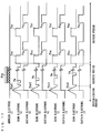
- Fig. 18 is a schematic view showing an example of a state where each of the discharge cells 14 in the sub-field SF1 lights up.
- Fig. 18 shows an example in which the states of the four discharge cells 14 provided on each of address electrodes 11a to 11d are "non-lighting", “lighting”, “non-lighting”, and "lighting” in descending order. In Fig. 18, only a part of the PDP 7 shown in Fig. 14 is illustrated.
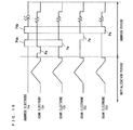
- Fig. 19 is a timing chart showing an example of respective driving voltages applied to the address electrode 11a and the scan electrodes 12a to 12d in the address time period in the sub-field SF1 when the discharge cells 14 on the PDP 7 are in the state shown in Fig. 18.
- the discharge cells 14 assume the state shown in Fig. 18 in the sub-field SF1
- the data pulse Pda is applied to the address electrode 11a in synchronization with the write pulse Pw applied to the scan electrode 12b
- the data pulse Pda is applied thereto in synchronization with the write pulse Pw applied to the scan electrode 12d, as shown in Fig. 19.
- address discharges are induced in each of the discharge cells 14 on an intersection of the address electrode 11a and the scan electrode 12b and the discharge cell 14 on an intersection of the address electrode 11a and the scan electrode 12d in Fig. 18, and the discharge cells 14 light up in the sustain time period.
- the data pulse Pda is also applied to the address electrodes 11b to 11d in synchronization with the write pulse Pw applied to the scan electrodes 12b and 12d, which is not illustrated.
- address discharges are induced in each of the discharge cells 14 on the scan electrodes 12b and 12d, and the discharge cells 14 light up in the sustain time period.
- Power is consumed at the time of the rise and the fall of the data pulse applied to each of the electrodes. Therefore, the power consumption is increased in proportion to the number of times of the rise and the number of times of the fall of the data pulse.
- driving pulses in a reset time period, an address time period, and a sustain time period are stopped for a sub-field in which no image bit information exists, which causes power consumption to be reduced.
- Patent Documents 2 to 4 are effective because all driving pulses are stopped for a sub-field in which a discharge cell enters a non-lighting state.
- power consumed in a sub-field in which a discharge cell enters a lighting state cannot be reduced.
- discharge cells alternately enter a lighting state and a non-lighting state as described above, the power consumption cannot be sufficiently reduced.
- the power consumption of a data driver is estimated by monitoring display data in a transition pattern, to perform such driving as to reduce a sub-field when the estimated power consumption is high.
- the power consumption can be also reduced in a sub-field in which a discharge cell enters a non-lighting state.
- the power consumption of the data electrode driver is monitored in a display pattern, so that the power consumption cannot be reduced only in a particular display pattern. For example, there are a case where the power consumption can be reduced and a case where it cannot be reduced depending on a transition pattern for display even if the respective numbers of pixels displayed on one screen in the cases are the same. That is, in the method disclosed in the above-mentioned Patent Document 5, the power consumption cannot, in some cases, be sufficiently reduced depending on the display pattern.
- An object of the present invention is to provide a display device capable of sufficiently reducing power consumption in various display patterns while preventing the image quality from being degraded and a method of driving the same.
- the information based on the number of the discharge cells that simultaneously light up out of the plurality of discharge cells in the first sub-field is detected.
- the first electrode is held at the constant potential in the address time period in the second sub-field depending on the detected information.
- Each of the plurality of gray levels is displayed in the combination of the respective emission or non-emission states in the plurality of sub-fields.
- the second sub-field has a lower weight than the weight of the first sub-field. In this case, when the number of the discharge cells that light up in the first sub-field increases, the average luminance level of an image increases, which makes it difficult to determine the difference between the luminance levels in the emission state and the non-emission state in the second sub-field.
- the potential of the first electrode is kept constant in the address time period in the second sub-field depending on the detected information.
- the respective numbers of the rise and the fall of the pulse applied to the first electrode are reduced in the address time period in the second sub-field, which allows the power consumed at the time of the rise and the fall of the pulse to be reduced.
- the potential of the first electrode is kept constant in the address time period in the second sub-field. Therefore, all the discharge cells enter the emission state or the non-emission state in the second sub-field irrespective of the image to be displayed, so that an error occurs in the luminance level of the image.
- the image quality is hardly degraded. The results allow the power consumption of the display device to be sufficiently reduced while preventing the image quality from being degraded.
- the potential of the first electrode is controlled on the basis of the number of the discharge cells that simultaneously light up in the first sub-field, which allows the power consumption to be reduced irrespective of a display pattern. That is, the power consumption of the display device can be sufficiently reduced in various display patterns.
- the power consumption of a display device can be sufficiently reduced in various display patterns while preventing the image quality from being degraded.
- Fig. 1 is a block diagram showing the configuration of a plasma display device according to a first embodiment of the present invention.
- a plasma display device shown in Fig. 1 comprises an A/D converter (Analog-to-Digital Converter) 1, a video signal/sub-field corresponder 2, a sub-field processor 3, a data driver 4, a scan driver 5, a sustain driver 6, a PDP (Plasma Display Panel) 7, a sub-field lighting rate measuring unit 8, and a blank signal generator 9.
- A/D converter Analog-to-Digital Converter
- sub-field processor 3 a data driver 4
- a scan driver 5 a sustain driver 6
- PDP Plasma Display Panel
- sub-field lighting rate measuring unit 8 a blank signal generator 9.
- An analog video signal VD is inputted to the A/D converter 1.
- the A/D converter 1 converts the analog video signal VD into digital image data, and outputs the digital image data to the video signal/sub-field corresponder 2.
- the video signal/sub-field corresponder 2 Since the video signal/sub-field corresponder 2 divides one field into a plurality of sub-fields to perform display, it generates image data SP corresponding to each of the sub-fields from image data corresponding to one field, and outputs the generated image data SP to the sub-field processor 3 and the sub-field lighting rate measuring unit 8.
- the sub-field lighting rate measuring unit 8 detects the respective lighting rates of discharge cells 14 simultaneously driven on the PDP 7 from the image data SP for each sub-field, and outputs the results of the detection to the blank signal generator 9 as a sub-field lighting rate signal SL.
- the sub-field lighting rate measuring unit 8 separately calculates the lighting rates in all the sub-fields using video signal information, which is decomposed into one-bit information representing lighting/non-lighting of the discharge cell 14 for each of the sub-fields, produced by the video signal/sub-field corresponder 2, and outputs the results of the calculation to the blank signal generator 9 as a sub-field lighting rate signal SL.
- the sub-field lighting rate measuring unit 8 contains a counter, and finds for each of the sub-fields the total number of the discharge cells 14 that light up by increasing the value of the counter one at a time when the video signal information decomposed into the one-bit information representing lighting/non-lighting indicates lighting, and divides the total number of the discharge cells 14 by the number of all the discharge cells 14 on the PDP 7, to find the lighting rate.
- the sub-field processor 3 generates a data driver driving control signal DS, a scan driver driving control signal CS, and a sustain driver driving control signal US from the image data SP for each of the sub-fields, and respectively outputs the signals to the data driver 4, the scan driver 5, and the sustain driver 6.
- the sub-field processor 3 outputs a sub-field number SN to the blank signal generator 9.
- the blank signal generator 9 generates a blank signal BLK on the basis of the sub-field lighting rate signal SL and the sub-field number SN, and outputs the generated blank signal BLK to the data driver 4.
- the PDP 7 comprises a plurality of address electrodes (data electrodes) 11, a plurality of scan electrodes 12, and a plurality of sustain electrodes 13.
- the plurality of address electrodes 11 are arranged in the vertical direction on a screen, and the plurality of scan electrodes 12 and the plurality of sustain electrodes 13 are arranged in the horizontal direction on the screen.
- the plurality of sustain electrodes 13 are commonly connected to one another.
- a discharge cell 14 is formed at each of intersections of the address electrodes 11, the scan electrodes 12, and the sustain electrodes 13. Each of the discharge cells 14 composes a pixel on the screen.
- the data driver 4 is connected to the plurality of address electrodes 11 in the PDP 7.
- the scan driver 5 contains a drive circuit provided for each of the scan electrodes 12, and each of the drive circuits is connected to the corresponding scan electrode 12 in the PDP 7.
- the sustain driver 6 is connected to the plurality of sustain electrodes 13 in the PDP 7.
- the data driver 4 applies a write pulse to the corresponding address electrode 11 in the PDP 7 in response to the image data SP in an address time period in accordance with the data driver driving control signal DS and the blank signal BLK.
- the scan driver 5 successively applies a write pulse to the plurality of scan electrodes 12 in the PDP 7 while shifting a shift pulse in a vertical scanning direction in the address time period in accordance with the scan driver driving control signal CS. This causes address discharges to be induced in the corresponding discharge cell 14.
- the scan driver 5 applies a periodical sustain pulse Psc to the plurality of scan electrodes 12 in the PDP 7 in a sustain time period in accordance with the scan driver driving control signal CS.
- the sustain driver 6 simultaneously applies a sustain pulse Psu whose phase is shifted by 180 degrees from the sustain pulse Psc in the scan electrode 12 to the plurality of sustain electrodes 13 in the PDP 7 in the sustain time period in accordance with the sustain driver driving control signal US. This causes sustain discharges to be induced in the corresponding discharge cell 14.
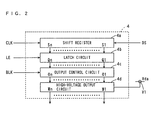
- Fig. 2 is a block diagram showing the configuration of the data driver 4 shown in Fig. 1.
- the data driver 4 shown in Fig. 2 comprises a shift register 4a, a latch circuit 4b, an output control circuit 4c, and a high-voltage output circuit 4d.
- a clock signal CLK is inputted from a clock generation circuit (not shown), and a data driver driving control signal DS is serially inputted from the sub-field processor 3 shown in Fig. 1.
- the shift register 4a converts the data driver driving control signal DS serially inputted into parallel driving control signals S1 to Sn and outputs the driving control signals S1 to Sn in response to the clock signal CLK. Note that n is an arbitrary integer.
- a latch enable signal LE is inputted from a latch enable signal generation circuit (not shown), and the driving control signals S1 to Sn are inputted from the shift register 4a.
- the latch circuit 4b respectively outputs the driving control signals S1 to Sn as driving control signals Q1 to Qn in response to the latch enable signal LE, and holds the driving control signals Q1 to Qn.
- a blank signal BLK is inputted from the blank signal generation circuit 9 shown in Fig. 1, and the driving control signals Q1 to Qn are inputted from the latch circuit 4b.
- the output control circuit 4c outputs the driving control signals Q1 to Qn as they are as output control signals O1 to On or outputs the output control signals O1 to On fixed to a low level.
- a power supply terminal V1 receiving a voltage Vda is connected to the high-voltage output circuit 4d.
- the output control signals O1 to On are inputted to the high-voltage output circuit 4d from the output control circuit 4c.
- the high-voltage output circuit 4d respectively outputs data signals W1 to Wn having a data pulse at the voltage Vda to the plurality of address electrodes 11 shown in Fig. 1 in response to the output control signals O1 to On.
- i is an arbitrary integer from 1 to n.
- Fig. 3 is a diagram for explaining the relationship among the driving control signal Qi, the blank signal BLK, the output control signal Oi, and the data signal Wi.
- the output control circuit 4c when the blank signal BLK is at a high level, the output control circuit 4c outputs the driving control signal Qi as it is as the output control signal Oi.
- the output control signal Oi has a pulse Po corresponding to a pulse Pq of the driving control signal Qi.
- the high-voltage output circuit 4d outputs the data signal Wi having a data pulse Pda at the voltage Vda to the address electrode 11 in response to the pulse Po of the output control signal Oi.
- the output control circuit 4c fixes the output control signal Oi to a low level.
- the data signal Wi does not have the data pulse Pda, and is held at 0 V.
- the level of the blank signal BLK is thus controlled, which makes it possible to choose whether or not the voltage Vda is applied to the address electrode 11.
- an ADS (Address Display-Period Separation) system is used as a gray scale expression driving system.
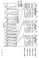
- Fig. 4 is a diagram for explaining the ADS system applied to the plasma display device shown in Fig. 1.
- Fig. 4 schematically shows driving voltages respectively applied to one sustain electrode 13, n scan electrodes 12, and one address electrode 11.
- Fig. 4 shows an example of a pulse of positive polarity for inducing discharges at the time of the rise of a driving waveform, the basic operation is the same as the following even in the case of a pulse of negative polarity for inducing discharges at the time of the fall thereof.
- one field is divided into sub-fields SF1 to SF11.
- Each of the sub-fields SF1 to SF11 is separated into an initialization time period T1, an address time period T2, and a sustain time period T3.
- the initialization operation of each of the sub-fields is performed in the initialization time period T1, address discharges for selecting the discharge cell 14 that lights up are induced in the address time period T2, and sustain discharges for display are induced in the sustain time period T3.
- an initialization setup pulse Pset is simultaneously applied to the plurality of scan electrodes 12.
- a write pulse Pw is successively applied to the plurality of scan electrodes 12, and a data pulse Pda is applied to the selected address electrode 11 in synchronization with the write pulse Pw.
- the initialization setup pulse Pset in the initialization time period T1 need not be applied to all the sub-fields but may be applied to some of the sub-fields.
- a sustain pulse Psc is applied to the plurality of scan electrodes 12, and a sustain pulse Psu is applied to the sustain electrode 13.
- the phase of the sustain pulse Psu is shifted by 180 degrees from the phase of the sustain pulse Psc. This causes sustain discharges to be induced in the discharge cell 14 that has induced address discharges in the address time period T2.
- the number of times the sustain pulses Psu and Psc are applied differs depending on the sub-field. Consequently, the number of times of sustain discharges induced in the sustain time period T3 differs depending on the sub-field. This causes each of the sub-fields SF1 to SF11 to be weighted.
- the shift in the phase between the sustain pulse Psu and the sustain pulse Psc need not be 180 degrees.
- respective parts of both the sustain pulses may be overlapped with each other on the time basis.
- the sustain pulse Psu is applied once to the sustain electrode 13, the sustain pulse Psc is applied once to the scan electrode 12, and the selected discharge cell 14 induces sustain discharges twice in the address time period T2.
- the sustain pulse Psu is applied twice to the sustain electrode 13
- the sustain pulse Psc is applied twice to the scan electrode 12
- the selected discharge cell 14 induces sustain discharges four times in the address time period T2.
- the sustain pulse Psu is applied four times to the sustain electrode 13
- the sustainpulse Psc is applied four times to the scan electrode 12, and the selected discharge cell 14 induces sustain discharges eight times in the address time period T2.
- the weights of the sub-fields SF1 to SF3 are respectively taken as 1, 2, and 4.
- Each of the gray levels can be displayed by combining respective emission or non-emission states in the sub-fields SF1 to SF11.
- the number of divisions into the sub-fields, the weight of each of the sub-fields, and the like are not particularly limited to those in the above-mentioned example, but can be subjected to various changes. Further, a time interval between the sub-fields need not be always constant but can be changed depending on the number of divisions into the sub-fields or the weight of each of the sub-fields.
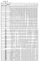
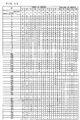
- Fig. 5 is a coding table showing an example of gray scale expression in the plasma display device according to the present embodiment.
- “1" to "11" in the first row in Fig. 5 respectively indicate sub-fields SF1 to SF11, and in the second row respectively indicate the weights of the sub-fields SF1 to SF11.
- figures in the leftmost column respectively indicate gray levels.
- “1" indicates the sub-field that enters the emission state
- "0" indicates the sub-field that does not enter the emission state.
- the weights of the sub-fields SF1 to SF11 are respectively 1, 2, 4, 6, 12, 22, 36, 60, 88, 120 and 160, and the weight of each of the sub-fields corresponds to the number of times of sustain discharges in the discharge cell 14 in the sustain time period T3 in the sub-field.
- each of the gray levels 0 to 511 is displayed by combining the respective emission or non-emission states in the sub-fields SF1 to SF11.
- sustain discharges are induced in each of the respective sustain time periods P3 in the sub-fields SF1, SF2, and SF3.
- a driving voltage applied to the address electrode 11 will be then described in detail.
- the sub-field SF3 does not enter the emission state until the gray level 4 is displayed, and the sub-field SF5 does not enter the emission state until the gray level 14 is displayed, for example.
- each of the sub-fields SF1 to SF10 does not enter the emission state until any one of the gray levels 1 to 351 is displayed, and the sub-field SF11 does not enter the emission state until the gray level 352 is displayed. That is, when combinations of emission and non-emission states in each of the sub-fields are arranged in the order in which the gray levels increase in the coding table shown in Fig. 5, the sub-field SF11 finally enters the emission state.
- the sub-field that finally enters the emission state when the combinations of emission and non-emission states in each of the sub-fields are arranged in the order in which the gray levels increase is referred to as a final sub-field LSF.
- the final sub-field LSF need not necessarily be positioned last on the time basis within one field.
- the lighting rate in each of the sub-fields is measured by the sub-field lighting rate measuring unit 8 shown in Fig. 1.
- the data pulse Pda is not applied to the address electrode 11 in the sub-field SF1 having the lowest weight in the same field.
- the discharge cell 14 does not light up in the sub-field SF1
- the average luminance level of an image (PDP7) is high when the lighting rate in the final sub-field LSF is high. Therefore, a viewer hardly feels the degradation of the image quality.
- the threshold value of the lighting rate makes it possible to prevent the image quality from being degraded because the sub-field SF1 does not enter the emission state.
- the threshold value of the lighting rate is 40 %, for example. Description is now made of the driving method using the drawings.
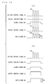
- Fig. 6 is a timing chart showing an example of signals and driving voltages in the sub-field SF1 in a case where the lighting rate in the final sub-field LSF does not exceed the threshold value
- Fig. 7 is a timing chart showing an example of signals and driving voltages in the sub-field SF1 in a case where the lighting rate in the final sub-field LSF exceeds the threshold value.
- Figs. 6 and 7 show an example of a driving voltage of one of the plurality of address electrodes 11. Further, the plurality of scan electrodes 12 are respectively assigned reference numerals 12 (1) to 12 (n) in order to distinguish their driving voltages.
- a driving control signal Qi having a plurality of pulses Pq is outputted from the latch circuit 4b shown in Fig. 2 in an address time period T2.
- the plurality of pulses Pq are respectively synchronized with write pulses Pw applied to the alternate scan electrodes 12 (1), 12 (3), ..., 12 (n).
- the blank signal generator 9 brings a blank signal BLK into a high level in the address time period T2, as shown in Fig. 6.
- the output control circuit 4c (see Fig. 3) outputs the driving control signal Qi as it is as an output control signal Oi.
- the output control signal Oi has pulses Po respectively corresponding to the pulses Pq of the driving control signal Qi.
- the high-voltage output circuit 4d (see Fig.
- the blank signal generator 9 maintains the blank signal BLK at a low level in the address time period T2, as shown in Fig. 7.
- the output control circuit 4c fixes the output control signal Oi to a low level in the address time period T2.
- the data signal Wi does not have the data pulses Pda, and is held at 0 V.
- the sub-field SF1 does not enter the emission state in all the discharge cells 14.
- the average luminance level of an image is high, so that a viewer hardly feels the degradation of the image quality.
- the data pulses Pda are not thus appliedto the address electrode 11 in the sub-field SF1 having the lowest weight in the same field. This allows the power consumption of the plasma display device to be sufficiently reduced while preventing the image quality from being degraded.
- the power consumption of the plasma display device can be reduced irrespective of a displaypattern. That is, the power consumption of the plasma display device can be sufficiently reduced in various display patterns.
- the sub-field in which the data pulses Pda are not applied is not limited to the sub-field SF1.
- the data pulses Pda need not be applied in the sub-fields SF1 and SF2, and the data pulses Pda need not be applied in the sub-fields SF1 to SF3.
- the threshold value is also adjusted, which allows the power consumption of the plasma display device to be sufficiently reduced in various display patterns while preventing the image from being degraded.
- a plasma display device differs from the plasma display device according to the first embodiment in the following points.
- Fig. 8 is a block diagram showing the configuration of the plasma display device according to the second embodiment of the present invention
- Fig. 9 is a block diagram showing the configuration of a data driver 4 shown in Fig. 8.
- a blank signal generator 9 generates a blank signal BLK and an output forcing signal PC on the basis of a sub-field lighting rate signal SL and a sub-field number SN, and outputs the generated signals to a data driver 4.
- the blank signal BLK and the output forcing signal PC are inputted to an output control circuit 4c in the data driver 4.
- the output control circuit 4c outputs driving control signals Q1 to Qn as they are as output control signals O1 to On, as output control signals O1 to On fixed to a low level, or as output control signals 01 to On fixed to a high level on the basis of the blank signal BLK and the output forcing signal PC.
- Fig. 10 is a diagram showing the relationship among the driving control signal Qi, the output forcing signal PC, the blank signal BLK, the output control signal Oi, and a data signal Wi.
- the output control circuit 4c when the output forcing signal PC is at a low level and the blank signal BLK is at a high level, the output control circuit 4c outputs the driving control signal Qi as it is as the output control signal Oi.
- the output control signal Oi has a pulse Po corresponding to a pulse Pq of the driving control signal Qi.
- the high-voltage output circuit 4d outputs the data signal Wi having a data pulse Pda at a voltage Vda to an address electrode 11 in response to the pulse Po of the output control signal Oi.
- the output control circuit 4c fixes the output control signal Oi to a high level.
- the data signal Wi is held at the voltage Vda.
- the data signal Wi is held at 0 V irrespective of the level of the output forcing signal PC, which is not illustrated.
- the respective levels of the output forcing signal PC and the blank signal BLK are thus controlled, which makes it possible to choose whether or not the voltage Vda is applied to the address electrode 11.
- Fig. 11 is a timing chart showing an example of signals and driving voltages in a sub-field SF1 in a case where the lighting rate in a final sub-field LSF exceeds a threshold value.
- the output control circuit 4c fixes the output control signal Oi to a high level in the address time period T2.
- the high voltage output circuit 4d fixes the data signal Wi to the voltage Vda in the address time period T2 and outputs the data signal Wi to the address electrode 11.
- the respective numbers of times of the rise and the fall of the data pulse Pda are one in the address time period T2, power consumed at the time of the rise and the fall of the data pulse Pda can be reduced.
- the sub-field SF1 enters an emission state in all discharge cells 14 when the lighting rate in the final sub-field LSF exceeds the threshold value.
- the average luminance level of an image is high, so that a viewer hardly feels the degradation of the image quality.
- the data pulse Pda for sustaining the voltage Vda is applied in the address time period T2 in the sub-field SF1 having the lowest weight in the same field. This allows the power consumption of the plasma display to be sufficiently reduced while preventing the image quality from being degraded.
- the power consumption of the plasma display device can be reduced irrespective of a display pattern. That is, the power consumption of the plasma display device can be sufficiently reduced in various display patterns.
- the sub-fields are arranged such that the weights thereof successively increase on the time axis of light emission, the sub-fields may be arranged as follows.
- Fig. 12 is a coding table showing another example of gray scale expression in a plasma display device.
- sub-fields can be partitioned into a first sub-field group comprising sub-fields SF1 to SF9 and a second sub-field group comprising sub-fields SF10 to SF14.
- the sub-fields SF1 to SF9 are arranged such that the weights thereof successively increase on the time axis.
- the sub-fields SF10 to SF14 are arranged such that the weights thereof successively increase on the time axis.
- the sub-fields in the second sub-field group enter an emission state subsequently to the sub-fields in the first sub-field group.
- the sub-field SF9 that does not enter the emission state when the gray level 327 and the preceding gray levels are displayed finally enters the emission state at the gray level 328. That is, in the coding table shown in Fig. 12, the sub-field SF9 becomes the final sub-field LSF.
- the data pulse Pda applied to the address electrode 11 is controlled on the basis of the lighting rate in the final sub-field LSF
- the data pulses Pda may be controlled on the basis of the number of times of lighting in the final sub-field LSF.
- the same effect as that in the foregoing case can be obtained by setting a threshold value of the number of times of lighting.
- the address electrode 11 corresponds to a first electrode
- the scan electrode 12 corresponds to a second electrode
- the sustain electrode 13 corresponds to a third electrode
- the sub-field lighting rate measuring unit 8 corresponds to detection means
- the final sub-field LSF corresponds to a first sub-field
- the sub-field SF1 corresponds to a second sub-field
- the first sub-field group and the second sub-field group correspond to a plurality of ranges.
- the present invention is applicable to display of various videos.
Landscapes
- Engineering & Computer Science (AREA)
- Physics & Mathematics (AREA)
- Computer Hardware Design (AREA)
- General Physics & Mathematics (AREA)
- Theoretical Computer Science (AREA)
- Plasma & Fusion (AREA)
- Power Engineering (AREA)
- Control Of Indicators Other Than Cathode Ray Tubes (AREA)
- Control Of Gas Discharge Display Tubes (AREA)
- Liquid Crystal Display Device Control (AREA)
Applications Claiming Priority (2)
| Application Number | Priority Date | Filing Date | Title |
|---|---|---|---|
| JP2005017399 | 2005-01-25 | ||
| PCT/JP2006/300645 WO2006080218A1 (ja) | 2005-01-25 | 2006-01-18 | 表示装置およびその駆動方法 |
Publications (2)
| Publication Number | Publication Date |
|---|---|
| EP1850313A1 true EP1850313A1 (de) | 2007-10-31 |
| EP1850313A4 EP1850313A4 (de) | 2009-10-21 |
Family
ID=36740252
Family Applications (1)
| Application Number | Title | Priority Date | Filing Date |
|---|---|---|---|
| EP06711914A Withdrawn EP1850313A4 (de) | 2005-01-25 | 2006-01-18 | Display-vorrichtung und verfahren zu ihrer ansteuerung |
Country Status (7)
| Country | Link |
|---|---|
| US (1) | US20090015516A1 (de) |
| EP (1) | EP1850313A4 (de) |
| JP (1) | JP4772033B2 (de) |
| KR (2) | KR20070096043A (de) |
| CN (1) | CN101107646B (de) |
| TW (1) | TW200636655A (de) |
| WO (1) | WO2006080218A1 (de) |
Cited By (1)
| Publication number | Priority date | Publication date | Assignee | Title |
|---|---|---|---|---|
| EP2264691A1 (de) * | 2009-06-18 | 2010-12-22 | Thomson Licensing | Verfahren und Vorrichtung zur Reduktion des Antriebsenergieverbrauchs |
Families Citing this family (7)
| Publication number | Priority date | Publication date | Assignee | Title |
|---|---|---|---|---|
| JP5003191B2 (ja) * | 2007-02-14 | 2012-08-15 | パナソニック株式会社 | プラズマディスプレイ装置の駆動方法 |
| US20130241972A1 (en) * | 2010-12-02 | 2013-09-19 | Panasonic Corporation | Method of driving plasma display device and plasma display device |
| KR101470296B1 (ko) * | 2011-07-13 | 2014-12-08 | 주식회사 실리콘웍스 | 저전압 차동신호 방식에서의 블랭크 구간 주기 감지방법 |
| US9501980B2 (en) * | 2011-12-28 | 2016-11-22 | Stmicroelectronics International N.V. | Display panel and display panel system |
| KR102056754B1 (ko) | 2018-05-18 | 2020-01-22 | (주)반도옵티칼 | 조립식 안경 |
| KR102465753B1 (ko) | 2020-07-29 | 2022-11-11 | (주) 명진아이웨어 | 안경테용 힌지 조립체 |
| TWI795857B (zh) * | 2021-08-02 | 2023-03-11 | 大陸商集創北方(珠海)科技有限公司 | 螢幕烙印避免方法及利用其之顯示器和資訊處理裝置 |
Family Cites Families (27)
| Publication number | Priority date | Publication date | Assignee | Title |
|---|---|---|---|---|
| JP3555995B2 (ja) * | 1994-10-31 | 2004-08-18 | 富士通株式会社 | プラズマディスプレイ装置 |
| JPH08223507A (ja) | 1995-02-20 | 1996-08-30 | Fujitsu General Ltd | 映像信号振幅制限回路 |
| US6100859A (en) * | 1995-09-01 | 2000-08-08 | Fujitsu Limited | Panel display adjusting number of sustaining discharge pulses according to the quantity of display data |
| JP3712802B2 (ja) * | 1996-10-29 | 2005-11-02 | 富士通株式会社 | 中間調表示方法および表示装置 |
| JPH10177365A (ja) | 1996-12-16 | 1998-06-30 | Victor Co Of Japan Ltd | プラズマディスプレイパネル表示装置の駆動制御装置 |
| JP3559135B2 (ja) | 1997-01-30 | 2004-08-25 | パイオニア株式会社 | プラズマディスプレイパネルの駆動方法 |
| JP3173469B2 (ja) * | 1998-08-19 | 2001-06-04 | 日本電気株式会社 | プラズマ表示方法及びプラズマ表示装置 |
| JP2000098972A (ja) | 1998-09-28 | 2000-04-07 | Matsushita Electric Ind Co Ltd | プラズマディスプレイパネル駆動装置 |
| TW516014B (en) * | 1999-01-22 | 2003-01-01 | Matsushita Electric Industrial Co Ltd | Driving method for AC plasma display panel |
| JP3915297B2 (ja) | 1999-01-22 | 2007-05-16 | 松下電器産業株式会社 | Ac型プラズマディスプレイパネルの駆動方法 |
| JP2001075529A (ja) * | 1999-09-07 | 2001-03-23 | Matsushita Electric Ind Co Ltd | 表示装置およびその輝度制御方法 |
| JP3369535B2 (ja) * | 1999-11-09 | 2003-01-20 | 松下電器産業株式会社 | プラズマディスプレイ装置 |
| US6900781B1 (en) * | 1999-11-12 | 2005-05-31 | Matsushita Electric Industrial Co., Ltd. | Display and method for driving the same |
| TW518555B (en) * | 2000-04-21 | 2003-01-21 | Matsushita Electric Industrial Co Ltd | Gray-scale image display device that can reduce power consumption when writing data |
| US6791515B2 (en) * | 2000-08-23 | 2004-09-14 | Matsushita Electric Industrial Co., Ltd. | Image display apparatus for writing display information with reduced electric consumption |
| JP2002156942A (ja) * | 2000-08-23 | 2002-05-31 | Matsushita Electric Ind Co Ltd | 画像表示装置 |
| US7050022B2 (en) * | 2000-09-13 | 2006-05-23 | Matsushita Electric Industrial Co., Ltd. | Display and its driving method |
| JP2004529389A (ja) | 2001-05-29 | 2004-09-24 | コーニンクレッカ フィリップス エレクトロニクス エヌ ヴィ | 画素を表示するディスプレイ駆動ユニット及び画素を表示する方法及びそのようなディスプレイ駆動ユニットを有する画像表示装置 |
| KR100467447B1 (ko) * | 2001-11-12 | 2005-01-24 | 삼성에스디아이 주식회사 | 플라즈마 디스플레이 패널의 화상 표시 방법 및 그 장치 |
| JP4308488B2 (ja) * | 2002-03-12 | 2009-08-05 | 日立プラズマディスプレイ株式会社 | プラズマディスプレイ装置 |
| JP4165108B2 (ja) * | 2002-04-12 | 2008-10-15 | 松下電器産業株式会社 | プラズマディスプレイ装置 |
| US20040061709A1 (en) * | 2002-09-17 | 2004-04-01 | Lg Electronics Inc. | Method and apparatus for driving plasma display panel |
| JP2004118084A (ja) * | 2002-09-27 | 2004-04-15 | Nec Corp | Ac型プラズマディスプレイパネルの駆動方法およびac型プラズマディスプレイパネル |
| JP2004151162A (ja) * | 2002-10-28 | 2004-05-27 | Nec Corp | 階調表示方法 |
| JP4050724B2 (ja) * | 2003-07-11 | 2008-02-20 | 松下電器産業株式会社 | 表示装置およびその駆動方法 |
| JP2005234369A (ja) * | 2004-02-20 | 2005-09-02 | Fujitsu Hitachi Plasma Display Ltd | 画像表示装置およびその駆動方法 |
| KR100560502B1 (ko) * | 2004-10-11 | 2006-03-14 | 삼성에스디아이 주식회사 | 플라즈마 표시 장치 및 그 구동 방법 |
-
2006
- 2006-01-18 CN CN2006800028706A patent/CN101107646B/zh not_active Expired - Fee Related
- 2006-01-18 EP EP06711914A patent/EP1850313A4/de not_active Withdrawn
- 2006-01-18 KR KR1020077019243A patent/KR20070096043A/ko not_active Ceased
- 2006-01-18 WO PCT/JP2006/300645 patent/WO2006080218A1/ja not_active Ceased
- 2006-01-18 KR KR1020087031977A patent/KR20090008481A/ko not_active Abandoned
- 2006-01-18 JP JP2007500469A patent/JP4772033B2/ja not_active Expired - Fee Related
- 2006-01-18 US US11/814,514 patent/US20090015516A1/en not_active Abandoned
- 2006-01-24 TW TW095102671A patent/TW200636655A/zh unknown
Cited By (3)
| Publication number | Priority date | Publication date | Assignee | Title |
|---|---|---|---|---|
| EP2264691A1 (de) * | 2009-06-18 | 2010-12-22 | Thomson Licensing | Verfahren und Vorrichtung zur Reduktion des Antriebsenergieverbrauchs |
| EP2264692A1 (de) * | 2009-06-18 | 2010-12-22 | Thomson Licensing | Verfahren und Vorrichtung zur Reduktion des Antriebsenergieverbrauchs |
| US8576216B2 (en) | 2009-06-18 | 2013-11-05 | Thomson Licensing | Method and apparatus for reducing driver energy consumption |
Also Published As
| Publication number | Publication date |
|---|---|
| JP4772033B2 (ja) | 2011-09-14 |
| CN101107646B (zh) | 2010-06-16 |
| WO2006080218A1 (ja) | 2006-08-03 |
| US20090015516A1 (en) | 2009-01-15 |
| TW200636655A (en) | 2006-10-16 |
| EP1850313A4 (de) | 2009-10-21 |
| JPWO2006080218A1 (ja) | 2008-06-19 |
| CN101107646A (zh) | 2008-01-16 |
| KR20070096043A (ko) | 2007-10-01 |
| KR20090008481A (ko) | 2009-01-21 |
Similar Documents
| Publication | Publication Date | Title |
|---|---|---|
| KR100737194B1 (ko) | 플라즈마 디스플레이 장치 | |
| EP1850313A1 (de) | Display-vorrichtung und verfahren zu ihrer ansteuerung | |
| CN100463035C (zh) | 等离子显示面板的驱动方法和等离子显示装置 | |
| KR100342280B1 (ko) | 표시 장치 및 그 구동 방법 | |
| CN101101725B (zh) | 等离子显示装置、等离子显示装置用驱动电路和等离子显示装置的图像显示方法 | |
| JP4318666B2 (ja) | プラズマ表示装置とその駆動方法 | |
| KR100884798B1 (ko) | 플라즈마 디스플레이 패널 및 그의 구동 방법 | |
| KR20090054229A (ko) | 플라즈마 표시 장치 및 그 구동 방법 | |
| JPH11265163A (ja) | Ac型pdpの駆動方法 | |
| KR100844834B1 (ko) | 플라즈마 디스플레이 장치의 구동방법 | |
| JP2002108278A (ja) | プラズマディスプレイ装置およびその駆動方法 | |
| KR20070042426A (ko) | 플라즈마 디스플레이 장치 및 그의 구동방법 | |
| KR100822213B1 (ko) | 플라즈마 디스플레이 패널 구동 방법 및 그 장치 | |
| EP1775704A1 (de) | Plasmaanzeigevorrichtung und Verfahren zu ihrer Ansteuerung | |
| KR100747169B1 (ko) | 플라즈마 디스플레이 장치 및 플라즈마 디스플레이 장치의구동 방법 | |
| KR100551016B1 (ko) | 플라즈마 표시 패널의 계조 표현 방법 및 플라즈마 표시장치 | |
| CN100426351C (zh) | 等离子显示设备及其驱动方法 | |
| KR100551066B1 (ko) | 플라즈마 표시 장치의 계조 표현 방법 및 플라즈마 표시장치 | |
| KR100603394B1 (ko) | 플라즈마 디스플레이 패널의 계조 확장 방법 | |
| EP1775701A2 (de) | Plasmaanzeigevorrichtung und Verfahren zu ihrer Ansteuerung | |
| CN100576298C (zh) | 等离子体显示器、控制装置及驱动方法 | |
| KR100553767B1 (ko) | 플라즈마 디스플레이 패널의 구동방법 및 구동장치 | |
| KR100637173B1 (ko) | 플라즈마 디스플레이 패널의 계조 확장 방법 | |
| KR20070087743A (ko) | 플라즈마 표시장치 및 그 구동방법 | |
| EP1923853A2 (de) | Plasmaanzeigevorrichtung und Verfahren zu ihrer Ansteuerung |
Legal Events
| Date | Code | Title | Description |
|---|---|---|---|
| PUAI | Public reference made under article 153(3) epc to a published international application that has entered the european phase |
Free format text: ORIGINAL CODE: 0009012 |
|
| 17P | Request for examination filed |
Effective date: 20070808 |
|
| AK | Designated contracting states |
Kind code of ref document: A1 Designated state(s): AT BE BG CH CY CZ DE DK EE ES FI FR GB GR HU IE IS IT LI LT LU LV MC NL PL PT RO SE SI SK TR |
|
| DAX | Request for extension of the european patent (deleted) | ||
| RAP1 | Party data changed (applicant data changed or rights of an application transferred) |
Owner name: PANASONIC CORPORATION |
|
| A4 | Supplementary search report drawn up and despatched |
Effective date: 20090918 |
|
| 17Q | First examination report despatched |
Effective date: 20100423 |
|
| STAA | Information on the status of an ep patent application or granted ep patent |
Free format text: STATUS: THE APPLICATION IS DEEMED TO BE WITHDRAWN |
|
| 18D | Application deemed to be withdrawn |
Effective date: 20120801 |