EP1852909A1 - Procédé d'integration d'une cellule de mémoire non-volatile dans un procédé CMOS à haute tension - Google Patents
Procédé d'integration d'une cellule de mémoire non-volatile dans un procédé CMOS à haute tension Download PDFInfo
- Publication number
- EP1852909A1 EP1852909A1 EP06009365A EP06009365A EP1852909A1 EP 1852909 A1 EP1852909 A1 EP 1852909A1 EP 06009365 A EP06009365 A EP 06009365A EP 06009365 A EP06009365 A EP 06009365A EP 1852909 A1 EP1852909 A1 EP 1852909A1
- Authority
- EP
- European Patent Office
- Prior art keywords
- forming
- oxide
- active area
- gate
- cmos transistor
- Prior art date
- Legal status (The legal status is an assumption and is not a legal conclusion. Google has not performed a legal analysis and makes no representation as to the accuracy of the status listed.)
- Withdrawn
Links
- 238000000034 method Methods 0.000 title claims abstract description 28
- 229910052581 Si3N4 Inorganic materials 0.000 claims abstract description 12
- HQVNEWCFYHHQES-UHFFFAOYSA-N silicon nitride Chemical compound N12[Si]34N5[Si]62N3[Si]51N64 HQVNEWCFYHHQES-UHFFFAOYSA-N 0.000 claims abstract description 12
- 238000004519 manufacturing process Methods 0.000 claims abstract description 7
- 230000003647 oxidation Effects 0.000 claims description 13
- 238000007254 oxidation reaction Methods 0.000 claims description 13
- 239000000758 substrate Substances 0.000 claims description 9
- 230000008719 thickening Effects 0.000 claims description 8
- 238000000151 deposition Methods 0.000 claims description 6
- 125000006850 spacer group Chemical group 0.000 claims description 5
- 238000002955 isolation Methods 0.000 claims description 3
- VYPSYNLAJGMNEJ-UHFFFAOYSA-N Silicium dioxide Chemical compound O=[Si]=O VYPSYNLAJGMNEJ-UHFFFAOYSA-N 0.000 claims description 2
- 229910052814 silicon oxide Inorganic materials 0.000 claims description 2
- 230000002542 deteriorative effect Effects 0.000 abstract 1
- 229910021420 polycrystalline silicon Inorganic materials 0.000 description 8
- 229920005591 polysilicon Polymers 0.000 description 8
- XUIMIQQOPSSXEZ-UHFFFAOYSA-N Silicon Chemical compound [Si] XUIMIQQOPSSXEZ-UHFFFAOYSA-N 0.000 description 5
- 229910052710 silicon Inorganic materials 0.000 description 5
- 239000010703 silicon Substances 0.000 description 5
- 230000015572 biosynthetic process Effects 0.000 description 3
- 230000007547 defect Effects 0.000 description 3
- 230000035876 healing Effects 0.000 description 3
- 230000008021 deposition Effects 0.000 description 2
- 230000001590 oxidative effect Effects 0.000 description 2
- 230000001419 dependent effect Effects 0.000 description 1
- 238000005516 engineering process Methods 0.000 description 1
- 230000006870 function Effects 0.000 description 1
- 230000000873 masking effect Effects 0.000 description 1
- 239000004065 semiconductor Substances 0.000 description 1
- 238000010561 standard procedure Methods 0.000 description 1
- 238000001039 wet etching Methods 0.000 description 1
Images

Classifications
-
- H—ELECTRICITY
- H10—SEMICONDUCTOR DEVICES; ELECTRIC SOLID-STATE DEVICES NOT OTHERWISE PROVIDED FOR
- H10B—ELECTRONIC MEMORY DEVICES
- H10B41/00—Electrically erasable-and-programmable ROM [EEPROM] devices comprising floating gates
- H10B41/40—Electrically erasable-and-programmable ROM [EEPROM] devices comprising floating gates characterised by the peripheral circuit region
- H10B41/42—Simultaneous manufacture of periphery and memory cells
- H10B41/49—Simultaneous manufacture of periphery and memory cells comprising different types of peripheral transistor
Definitions
- the invention relates to a process for manufacturing a device comprising at least one MOS FET transistor and a non-volatile memory cell. Such devices are useful for programmable logic circuits especially for ASICS.
- the intermediate dielectric between floating gate and control gate needs a good control of oxide thickness.
- the polysilicon floating gates of the EEPROM will oxidize during the oxide growth process of the CMOS structure and thus the EEPROM high voltage gate oxide regions will end up with a too thick oxide slowing down the maximum operation speed of the EEPROM. It is further necessary that processing the EEPROM cell does not deteriorate the oxide quality of the CMOS structure.
- the formation of the EEPROM cell has to take place before the gate oxide growth e.g. a high voltage gate oxide.
- a gate oxide growth e.g. a high voltage gate oxide.
- this protection is achieved by covering these regions with a non oxidizing protection layer (e.g. silicon nitride) to prevent oxidation. After the growth of the high voltage gate oxide the protection layer can be removed and the normal manufacturing process flow of the CMOS structure is continued.
- the proposed manufacturing process comprises the following steps which can be successfully performed in the given sequence:
- the gate oxides have to suffer only the step of stripping of resists and of removing said silicon nitride layer. Structuring of the floating gate is performed before the gate oxide formation to spare the gate oxides the polysilicon etch.
- all oxides produced are subjected to a common thermal oxidation step thereby healing possible defects in the oxide structures and raising the thickness of the oxide structures to the desired values.
- a further oxide of a thickness which is small with respect to the other gate oxides may be formed on a silicon surface in a third active area. The healing of the oxides is performed until the desired thickness of the oxide in the third active area is reached.
- All oxide forming processes i.e. the steps of forming the tunnel oxide, the intermediate dielectric and the gate oxide of the CMOS transistor may be performed by thermal oxidation. It is also possible to form a part of the total oxide thickness by vapour or plasma deposition. In these cases it is preferred that the last step forming the oxides is a thermal oxidation step healing all possible defects which may be produced during oxide deposition.
- At least a third active area is formed for producing a second or a further CMOS transistor therein.
- the step of forming the gate oxide of the CMOS transistor may comprise the following steps
- the oxide thickness in the second active area is thus the sum of the first oxide layer thickness and the amount resulting from thickening. While removing the first oxide layer in the third active area, it is possible to stop this removing, which is usually a wet etching step but may be also a dry etch step, at a given remaining oxide layer thickness. But totally removing the oxide layer is a process which can be better controlled. Stripping the resist does not deteriorate the oxide quality there below. The more so as the following oxidation step heals any defects.
- This step sequence results in different oxide layer thicknesses in the second and the third active area providing different gate oxides for different transistors operating at different voltages.
- One of the transistors may be a high voltage transistor working at a voltage of 20V for example. This transistor can be used as a selection transistor for the EEPROM cell. According to the desired functions of the device the operating voltage may even be higher.
- the transistor formed in the second active area is the transistor operating with the highest voltage as this transistor can be processed with the highest gate oxide thickness.
- a further step of a thermal oxidation to densify the intermediate dielectric can follow. This step can be combined with the before mentioned step of thickening the oxide layer in the second and forming the (new) the oxide in the third active area.
- the total process starts with defining the active areas of the transistors and other structures to be produced in the substrate.
- Field oxide areas are produced by thermal oxidation of the substrate.
- the active areas which are to be prevented from oxidation are covered with a protection layer usually a silicon nitride layer.
- a protection layer usually a silicon nitride layer.
- the Field oxide areas are surrounding the active areas and each active area is defined and isolated against adjacent active areas by this field oxide.
- shallow trench isolation can be used to define the active areas.
- Wells in the semiconductor substrate may be formed before and/or after the field oxide formation for isolating the transistors to be produced later therein against substrate.
- the gates are produced. This can be done by depositing a polysilicon layer and structuring the layer.
- Next step is forming the polysilicon 2 plane comprising the steps of depositing a layer of polysilicon in a thickness necessary for the control gate of the EEPROM cell, structuring the polysilicon 2 layer and forming spacers at the side edges of the multilayer stack comprising floating gate, intermediate dielectric and control gate as well as at the gates of the CMOS transistors.
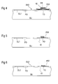
- Figure 1 to 7 show schematic cross sections of an electronic device at different stages of processing.
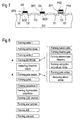
- FIG. 8 shows the sequence of process modules.
- Isolating wells for the transistor structures are formed in a silicon substrate SU (not shown in the figures). Then at least three active areas AA1, AA2 and AA3 are defined by forming field oxide areas FO or shallow trench isolations (not shown in the figure).
- a thin tunnel oxide TO for the EEPROM cell is formed and structured to remain in the first active area AA1 only.
- a first polysilicon layer is deposited and structured to form the floating gate PS1 in the first active area AA1.
- the intermediate dielectric IO is produced by thermal growth and depositing silicon oxide up to a first thickness and then thickening it to a second thickness. The oxide is then masked and etched back to remain only in the first active area AA1.
- Figure 1 shows the device after this step.
- a silicon nitride protection layer SN is deposited and structured to only cover the first active area AA1.
- a first oxide layer OL1 is formed in the remaining active areas AA2 and AA3 where the silicon of the substrate SU is exposed.
- Figure 2 shows the device after this step.
- a resist layer RL is produced to cover only the oxide layer OL1 in the second active area AA2 as shown in figure 3. Exposed areas of the oxide layer OL1 are then removed by wet etch or plasma etch to expose the silicon surface in the third active area AA3.
- Figure 4 shows the device after stripping the resist RL1.
- Figure 5 shows the device after removing the silicon nitride SN. Exposed silicon substrate in the third active area AA3 is oxidized to produce a third oxide layer OL3 there. Remaining first oxide OL1 and intermediate dielectric are thickened up by this step.
- Figure 6 shows the device after this step showing a oxide layer OL2 of a second higher thickness in the first active area and a newly formed third oxide layer OL3 of a third small thickness in the third active area AA3.
- Figure 7 shows the device after proceeding further steps as already described above.
- second and third active area AA2 two CMOS transistors have been completed by forming gates G2, G3, spacers SP2, SP3 and by doping source and drain regions S,D. Different gate oxide thickness allows to operate these two transistors with different voltages.
- the control gate PS2 and further spacers SP1 are formed.
- Figure 8 shows the sequence of process modules necessary to manufacture the device comprising at least one CMOS structure and a EEPROM cell.
- the modules are listed of which the two modules characterized with an asterix are new (first module) or modified (second module) with respect to a known CMOS process sequence. These new modules each comprise a series of different steps which are listed in the right column.
- transistors which may have a deviating gate oxide thickness may be formed according to the given process sequence.
- the arrangement of the device areas may be different and comprise further structure elements not belonging to the mentioned one but part of the circuit formed in the device.
Landscapes
- Engineering & Computer Science (AREA)
- Manufacturing & Machinery (AREA)
- Metal-Oxide And Bipolar Metal-Oxide Semiconductor Integrated Circuits (AREA)
- Semiconductor Memories (AREA)
- Non-Volatile Memory (AREA)
Priority Applications (1)
| Application Number | Priority Date | Filing Date | Title |
|---|---|---|---|
| EP06009365A EP1852909A1 (fr) | 2006-05-05 | 2006-05-05 | Procédé d'integration d'une cellule de mémoire non-volatile dans un procédé CMOS à haute tension |
Applications Claiming Priority (1)
| Application Number | Priority Date | Filing Date | Title |
|---|---|---|---|
| EP06009365A EP1852909A1 (fr) | 2006-05-05 | 2006-05-05 | Procédé d'integration d'une cellule de mémoire non-volatile dans un procédé CMOS à haute tension |
Publications (1)
| Publication Number | Publication Date |
|---|---|
| EP1852909A1 true EP1852909A1 (fr) | 2007-11-07 |
Family
ID=37055769
Family Applications (1)
| Application Number | Title | Priority Date | Filing Date |
|---|---|---|---|
| EP06009365A Withdrawn EP1852909A1 (fr) | 2006-05-05 | 2006-05-05 | Procédé d'integration d'une cellule de mémoire non-volatile dans un procédé CMOS à haute tension |
Country Status (1)
| Country | Link |
|---|---|
| EP (1) | EP1852909A1 (fr) |
Cited By (1)
| Publication number | Priority date | Publication date | Assignee | Title |
|---|---|---|---|---|
| CN114335179A (zh) * | 2020-09-30 | 2022-04-12 | 意法半导体(鲁塞)公司 | 三栅极mos晶体管及此类晶体管的制造方法 |
Citations (4)
| Publication number | Priority date | Publication date | Assignee | Title |
|---|---|---|---|---|
| EP0610643A1 (fr) * | 1993-02-11 | 1994-08-17 | STMicroelectronics S.r.l. | Cellule EEPROM et transistor MOS périphérique |
| US5911104A (en) * | 1998-02-20 | 1999-06-08 | Texas Instruments Incorporated | Integrated circuit combining high frequency bipolar and high power CMOS transistors |
| US5911105A (en) * | 1996-07-12 | 1999-06-08 | Nec Corporation | Flash memory manufacturing method |
| US6689653B1 (en) * | 2003-06-18 | 2004-02-10 | Chartered Semiconductor Manufacturing Ltd. | Method of preserving the top oxide of an ONO dielectric layer via use of a capping material |
-
2006
- 2006-05-05 EP EP06009365A patent/EP1852909A1/fr not_active Withdrawn
Patent Citations (4)
| Publication number | Priority date | Publication date | Assignee | Title |
|---|---|---|---|---|
| EP0610643A1 (fr) * | 1993-02-11 | 1994-08-17 | STMicroelectronics S.r.l. | Cellule EEPROM et transistor MOS périphérique |
| US5911105A (en) * | 1996-07-12 | 1999-06-08 | Nec Corporation | Flash memory manufacturing method |
| US5911104A (en) * | 1998-02-20 | 1999-06-08 | Texas Instruments Incorporated | Integrated circuit combining high frequency bipolar and high power CMOS transistors |
| US6689653B1 (en) * | 2003-06-18 | 2004-02-10 | Chartered Semiconductor Manufacturing Ltd. | Method of preserving the top oxide of an ONO dielectric layer via use of a capping material |
Cited By (2)
| Publication number | Priority date | Publication date | Assignee | Title |
|---|---|---|---|---|
| CN114335179A (zh) * | 2020-09-30 | 2022-04-12 | 意法半导体(鲁塞)公司 | 三栅极mos晶体管及此类晶体管的制造方法 |
| US12125913B2 (en) | 2020-09-30 | 2024-10-22 | STMicroelectronicsa (Rousset) SAS | Triple-gate MOS transistor and method for manufacturing such a transistor |
Similar Documents
| Publication | Publication Date | Title |
|---|---|---|
| US7687387B2 (en) | Semiconductor device and method of manufacturing the same | |
| JP2002343879A (ja) | 半導体装置及びその製造方法 | |
| US6462370B2 (en) | Integrated circuit memory devices having non-volatile memory transistors and methods of fabricating the same | |
| US8325516B2 (en) | Semiconductor device with split gate memory cell and fabrication method thereof | |
| US6787419B2 (en) | Method of forming an embedded memory including forming three silicon or polysilicon layers | |
| US20040147099A1 (en) | Method of producing semiconductor device | |
| JP2008244352A (ja) | 半導体装置 | |
| JP2003060094A (ja) | 不揮発性半導体記憶装置の製造方法 | |
| EP1852909A1 (fr) | Procédé d'integration d'une cellule de mémoire non-volatile dans un procédé CMOS à haute tension | |
| US8034695B2 (en) | Semiconductor device and method of manufacturing the same | |
| US8450199B2 (en) | Integrating diverse transistors on the same wafer | |
| JP4098208B2 (ja) | 半導体装置の製造方法 | |
| JP5141069B2 (ja) | 半導体装置 | |
| US7556999B2 (en) | Method for fabricating non-volatile memory | |
| US7910444B2 (en) | Process for forming differential spaces in electronics device integrated on a semiconductor substrate | |
| US8927370B2 (en) | Method for fabricating memory | |
| JP2000353796A (ja) | 半導体装置およびその製造方法 | |
| KR100580581B1 (ko) | 반도체 장치의 제조 방법 | |
| KR101128698B1 (ko) | 고전압 트랜지스터 및 이를 구비한 반도체 소자의 제조방법 | |
| KR100511898B1 (ko) | 반도체 소자의 제조방법 | |
| JP2007012779A (ja) | 半導体装置およびその製造方法 | |
| JP4989076B2 (ja) | 半導体装置の製造方法 | |
| JP2005294739A (ja) | 半導体記憶装置の製造方法 | |
| US20050112824A1 (en) | Method of forming gate oxide layers with multiple thicknesses on substrate | |
| JP5458547B2 (ja) | 半導体装置の製造方法 |
Legal Events
| Date | Code | Title | Description |
|---|---|---|---|
| PUAI | Public reference made under article 153(3) epc to a published international application that has entered the european phase |
Free format text: ORIGINAL CODE: 0009012 |
|
| AK | Designated contracting states |
Kind code of ref document: A1 Designated state(s): AT BE BG CH CY CZ DE DK EE ES FI FR GB GR HU IE IS IT LI LT LU LV MC NL PL PT RO SE SI SK TR |
|
| AX | Request for extension of the european patent |
Extension state: AL BA HR MK YU |
|
| AKX | Designation fees paid | ||
| STAA | Information on the status of an ep patent application or granted ep patent |
Free format text: STATUS: THE APPLICATION IS DEEMED TO BE WITHDRAWN |
|
| 18D | Application deemed to be withdrawn |
Effective date: 20080508 |
|
| REG | Reference to a national code |
Ref country code: DE Ref legal event code: 8566 |