EP1852911B1 - Dispositif a semi-conducteur - Google Patents
Dispositif a semi-conducteur Download PDFInfo
- Publication number
- EP1852911B1 EP1852911B1 EP06714028.5A EP06714028A EP1852911B1 EP 1852911 B1 EP1852911 B1 EP 1852911B1 EP 06714028 A EP06714028 A EP 06714028A EP 1852911 B1 EP1852911 B1 EP 1852911B1
- Authority
- EP
- European Patent Office
- Prior art keywords
- region
- semiconductor
- semiconductor element
- transistor
- ratio
- Prior art date
- Legal status (The legal status is an assumption and is not a legal conclusion. Google has not performed a legal analysis and makes no representation as to the accuracy of the status listed.)
- Expired - Lifetime
Links
Images



Classifications
-
- H—ELECTRICITY
- H10—SEMICONDUCTOR DEVICES; ELECTRIC SOLID-STATE DEVICES NOT OTHERWISE PROVIDED FOR
- H10D—INORGANIC ELECTRIC SEMICONDUCTOR DEVICES
- H10D12/00—Bipolar devices controlled by the field effect, e.g. insulated-gate bipolar transistors [IGBT]
- H10D12/411—Insulated-gate bipolar transistors [IGBT]
- H10D12/441—Vertical IGBTs
-
- H—ELECTRICITY
- H10—SEMICONDUCTOR DEVICES; ELECTRIC SOLID-STATE DEVICES NOT OTHERWISE PROVIDED FOR
- H10W—GENERIC PACKAGES, INTERCONNECTIONS, CONNECTORS OR OTHER CONSTRUCTIONAL DETAILS OF DEVICES COVERED BY CLASS H10
- H10W90/00—Package configurations
-
- H—ELECTRICITY
- H10—SEMICONDUCTOR DEVICES; ELECTRIC SOLID-STATE DEVICES NOT OTHERWISE PROVIDED FOR
- H10W—GENERIC PACKAGES, INTERCONNECTIONS, CONNECTORS OR OTHER CONSTRUCTIONAL DETAILS OF DEVICES COVERED BY CLASS H10
- H10W90/00—Package configurations
- H10W90/701—Package configurations characterised by the relative positions of pads or connectors relative to package parts
- H10W90/751—Package configurations characterised by the relative positions of pads or connectors relative to package parts of bond wires
- H10W90/753—Package configurations characterised by the relative positions of pads or connectors relative to package parts of bond wires between laterally-adjacent chips
-
- H—ELECTRICITY
- H10—SEMICONDUCTOR DEVICES; ELECTRIC SOLID-STATE DEVICES NOT OTHERWISE PROVIDED FOR
- H10W—GENERIC PACKAGES, INTERCONNECTIONS, CONNECTORS OR OTHER CONSTRUCTIONAL DETAILS OF DEVICES COVERED BY CLASS H10
- H10W90/00—Package configurations
- H10W90/701—Package configurations characterised by the relative positions of pads or connectors relative to package parts
- H10W90/751—Package configurations characterised by the relative positions of pads or connectors relative to package parts of bond wires
- H10W90/756—Package configurations characterised by the relative positions of pads or connectors relative to package parts of bond wires between a chip and a stacked lead frame, conducting package substrate or heat sink
Definitions
- the present invention relates to a semiconductor device in which a plurality of semiconductor elements are mounted on a single support substrate.
- an H-shaped bridge circuit 80 shown in FIG. 8 is used.
- the H-shaped bridge circuit 80 comprises a first transistor 81 and third transistor 83 at a high side, and a second transistor 82 and fourth transistor 84 at a low side.
- a load 86 such as, for example, a cold cathode fluorescent discharge tube, etc. is connected between a connection node A1 between the emitter electrode of the first transistor 81 and the collector electrode of the second transistor 82, and a connection node A2 between the emitter of the third transistor 83 and the collector of the fourth transistor 84.
- a control circuit 85 switches on or off the first transistor 81 and fourth transistor 84, and the second transistor 82 and third transistor 83 alternately in the H-shaped bridge circuit 80, a current flows across the connection node A1 and the connection node A2 alternately, thereby enabling the load 86 to operate. In this manner, a direct-current voltage is converted into an alternating current in the H-shaped bridge circuit 80, making it possible to light, for example, a cold cathode fluorescent discharge tube.
- the semiconductor device according to the stacking method disclosed in the above-indicated Unexamined Japanese Patent Application KOKAI Publication No. S55-111151 has a possibility of its elements being ruined, due to occurrence of a thermal runaway, because heat emitted from the semiconductor elements during operation is not radiated favorably.
- semiconductor elements placed on lower levels easily gather heat, due to heat generated during operation and heat transmitted from the semiconductor elements stacked on upper levels, thus easily cause a thermal runaway.
- the present invention is made in view of the above-described circumstance, and an object of the present invention is to provide a semiconductor device which has a favorable heat radiation performance.
- a semiconductor device comprises:
- the first region is formed so as to correspond to a region where the second semiconductor element is placed.
- the first region is formed to have generally a same area as the second semiconductor element.
- the first semiconductor element and the second semiconductor element may be switched alternately.
- a heat radiation layer may be formed between the first semiconductor element and the second semiconductor element.
- the second semiconductor region may be formed in a belt shape.
- An impurity concentration of the second semiconductor region may be relatively high in the first region of the semiconductor base, and relatively low in the second region.
- the semiconductor device may further comprise a first electrode formed on the second semiconductor region via an insulating film, and a film thickness of the insulating film may be relatively thick in the first region of the semiconductor base, and relatively thin in the second region.
- the semiconductor base may further comprise a third region formed between the first region and the second region, and a rate at which the third semiconductor region in the third region occupies the second semiconductor region may be higher than the first rate and lower than the second rate.
- the second semiconductor element may comprise a semiconductor base which comprises: a fourth semiconductor region of the first conductivity type; a fifth semiconductor region of the second conductivity type formed in a surface region of the fourth semiconductor region; and a sixth semiconductor region of the first conductivity type formed in a surface region of the fifth semiconductor region, and the semiconductor base of the second semiconductor element may comprise: a fourth region formed at a center part of the semiconductor base with a fourth rate of the sixth semiconductor region with respect to the fifth semiconductor region; and a fifth region in which the sixth semiconductor region occupies the fifth semiconductor region at a fifth rate higher than the fourth rate and which is formed in an annular shape at a circumferential part of the semiconductor base so as to surround the fourth region.
- a semiconductor device comprising: a support substrate; a first semiconductor element placed on the support substrate; a second semiconductor element placed on the first semiconductor element; a third semiconductor element formed on the support substrate; and a fourth semiconductor element placed on the third semiconductor element,
- the first region of the first semiconductor element may be formed in a region where the second semiconductor element is placed, and the first region of the third semiconductor element may be formed in a region where the fourth semiconductor element is placed.
- a heat radiation layer may be formed between the first semiconductor element and the second semiconductor element, and between the third semiconductor element and the fourth semiconductor element.
- a semiconductor element for a controlling purpose may further be formed on the support substrate, and the first semiconductor element and the fourth semiconductor element, and the second semiconductor element and the third semiconductor element may be switched alternately by the semiconductor element for the controlling purpose.
- a semiconductor device comprising: a first semiconductor element placed on a support substrate; and a second semiconductor element placed on the first semiconductor element and having a semiconductor region which faces a semiconductor region of the first semiconductor element,
- a semiconductor device is a semiconductor device, comprising a plurality of semiconductor elements sequentially stacked on a support substrate,
- IGBT insulated gate bipolar transistors
- FIG. 1 is a plan view showing the semiconductor device 10.
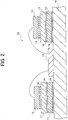
- FIG. 2 is a cross sectional view of the semiconductor device 10 shown in FIG. 1 as taken along a line X-X'.
- the semiconductor device 10 according to the present invention constitutes the H-shaped bridge circuit 80 shown in FIG. 8
- the semiconductor device 10 comprises a first transistor 11, a second transistor 12, a third transistor 13, a fourth transistor 14, a control circuit 15, a substrate 16, heat radiation layers 17, and solder layers 18, and is sealed by a resin sealing body 21, as shown in FIG. 1 and FIG. 2 .
- the first transistor 11, the second transistor 12, the third transistor 13, and the fourth transistor 14 each comprise an IGBT, and perform switching operations by the control circuit 15.
- the first transistor 11 is placed on the substrate 16 via the solder layer 18 as shown in FIG. 2 .
- the emitter regions of the first transistor 11 comprise a first region formed at the center part of the first transistor 11, and a second region formed at the peripheral part of the first transistor 11 so as to surround the first region.
- the first region of the emitter regions has generally the same area as that of the second transistor 12, and is formed so as to correspond to the position at which the second transistor 12 is placed.
- the first region and second region of the emitter regions have different rates of area occupied in the base regions. The rate of area occupied in the base regions in the first region is smaller, as compared with the second region.
- the second transistor 12 is placed, via the solder layer 18, on the heat radiation layer 17, which is placed on the first transistor 11 via the solder layer 18.
- the first transistor 11 and the second transistor 12 are electrically connected via the heat radiation layer 17.
- the second transistor 12 is formed to have a uniform area distribution for its emitter regions.
- the third transistor 13 is disposed on the substrate 16 via the solder layer 18, as shown in FIG. 2 .
- the emitter regions of the third transistor 13 comprise a first region formed at the center part of the third transistor 13 and a second region formed at the peripheral part of the first transistor 13 so as to surround the first region.
- the first region has generally the same area as that of the fourth transistor 14, and is formed so as to correspond to the position at which the second transistor 12 is placed.
- the first region and second region of the emitter regions have different rates of area occupied in the base regions. The rate of area occupied in the base regions in the first region is smaller, as compared with the second region.
- the fourth transistor 14 is placed, via the solder layer 18, on the heat radiation layer 17, which is placed on the third transistor 13 via the solder layer 18, as shown in FIG. 2 .
- the third transistor 13 and the fourth transistor 14 are electrically connected via the heat radiation layer 17.
- the fourth transistor 14 is also formed to have a uniform area distribution for its emitter regions.
- the control circuit 15 is connected to the gate electrode of each of the first transistor 11 to the fourth transistor 14, as shown in FIG. 1 .
- Each transistor is switched to be on or off by the control circuit 15, such that the second transistor 12 and the third transistor 13 are off when the first transistor 11 and the fourth transistor 14 are on, and the second transistor 12 and the third transistor 13 are on when the first transistor 11 and the fourth transistor 14 are off.
- an alternating current flows through the load 86 of the H-shaped bridge circuit 80 shown in FIG. 8 .
- the substrate 16 is formed of a metal plate of copper, aluminum, or the like. Heat emitted from the first transistor 11 and third transistor 13 is radiated via the substrate 16.
- the heat radiation layers 17 are formed of a metal plate of copper, aluminum, or the like, and formed between the first transistor 11 and the second transistor, and between the third transistor 13 and the fourth transistor 14. Heat emitted from the respective transistors is transmitted to the heat radiation layers 17 via the solder layers 18 and radiated therefrom.
- the heat radiation layers 17 may be formed not only of a metal plate, but of a thin solder layer.
- the first transistor 11 will specifically be explained by using FIG. 3 to FIG. 6 . Since the third transistor 13 has the same configuration as that of the first transistor 11 except that the first region of the emitter region thereof is formed to correspond to the region where the fourth transistor 14 is placed, explanation will be given by employing only the first transistor 11 as an example.
- FIG. 3 is a plan view showing an example of the structure of the first transistor 11.
- FIG. 4 is a plan view showing a region 11a enclosed by a dashed line in the first transistor 11 shown in FIG. 3 .
- FIG. 5 is a plan view showing a region 11b enclosed by a dashed line in the first transistor 11 shown in FIG. 3 .
- FIG. 6 is a cross sectional view of the first transistor 11 shown in FIG. 4 as taken along Y-Y'.
- an emitter electrode 35, gate electrodes 37, and interlayer insulating films 39 which are to be described later, are omitted, and the shapes of the N type emitter regions 33 are illustrated as rectangles unlike in FIG. 4 and FIG. 5 .
- the emitter electrode 35 to be described later is omitted.
- the first transistor 11 comprises a semiconductor base 41, an emitter electrode 35, a collector electrode 36, gate electrodes 37, gate insulating films 38, and interlayer insulating films 39.
- the semiconductor base 41 comprises an N type base region 30, a P type collector region 31, P type base regions 32, N type emitter regions 33, and an N type buffer region 34.
- the N type base region 30 is formed of an N type semiconductor region in which an N type (first conductivity type) impurity such as, for example, phosphorus or the like is diffused.
- the N type base region 30 is formed to have a thickness of, for example, about 45 ⁇ m and an impurity concentration of about 2 ⁇ 10 14 cm -3 .
- the P type collector region 31 is formed of a P type semiconductor region in which a P type (second conductivity type) impurity such as, for example, boron or the like is diffused, and is formed on the lower surface of the N type buffer region 34 as shown in FIG. 6 .
- the collector electrode 36 is formed on the lower surface of the P type collector region 31. While the first transistor 11 is operating, the P type collector region 31 injects holes (positive holes) into the N type base region 30 and brings about conductivity modulation.
- the P type collector region 31 is formed to have a thickness of, for example, about 200 ⁇ m.
- the P type impurity concentration of the P type collector region 31 is higher than the impurity concentration of the P type base regions 32, and formed to be an impurity concentration of, for example, about 4 ⁇ 10 18 cm -3 .
- the P type base regions 32 are formed of a P type semiconductor region in which a P type impurity is diffused, and are formed in the surface regions of the N type base region 30 as shown in FIG. 6 .
- the P type base regions 32 are formed in a belt shape as shown in FIG. 6 , and formed side by side so as to be spaced apart from each other.
- the gate electrodes 37 are formed, via the gate insulating films 38, on the P type base regions 32, which are between the N type base region 30 and the N type emitter regions 33. When a voltage equal to or greater than a threshold voltage is applied to the gate electrodes 37, channels are formed in the P type base regions 32.
- the P type base regions 32 are formed to have a thickness of, for example, about 3 ⁇ m.
- the P type impurity concentration of the P type base regions 32 is lower than the impurity concentration of the P type collector region 31, and formed to be an impurity concentration of, for example, about 2 ⁇ 10 17 cm -3 .
- the N type emitter regions 33 are formed of an N type semiconductor region in which an N type impurity is diffused, and are formed in the surface regions of the P type base regions 32.
- the emitter electrode 35 is formed on the upper surface of the N type emitter regions 33 as shown in FIG. 6 .
- the N type emitter regions 33 are formed to have a thickness of, for example, about 0.5 ⁇ m.
- the N type impurity concentration of the N type emitter regions 33 is higher than the N type base region 30, and formed to be an impurity concentration of, for example, about 5 ⁇ 10 19 cm -3 .
- the N type emitter regions 33 comprises a first region which is formed at the center part of the first transistor 11 and in which the N type emitter regions 33 have a low rate of occupation in the P type base regions 32, and a second region which is formed so as to surround the first region and in which the N type emitter regions 33 have a higher rate of occupation in the P type base regions 32 as compared with the first region.
- the first region of the N type emitter regions 33 is formed so as to correspond to the region at which the second transistor 12 is placed.
- the center part of the first transistor 11, at which the first region of the N type emitter regions 33 is formed is constructed such that a width Te1 of the N type emitter regions 33 under the gate electrodes 37 and interlayer insulating films 39 is 3 ⁇ m, a width Te2 of the N type emitter regions 33 under the emitter electrode 35 is 4.5 ⁇ m, an interval De1 between adjoining N type emitter regions 33 under the interlayer insulating film 39 is 12 ⁇ m, and an interval De2 between adjoining N type emitter regions 33 under the emitter electrode 35 is 10.5 ⁇ m, as shown in FIG. 4 .
- the peripheral part of the first transistor 11, at which the second region of the N type emitter regions 33 is formed is constructed such that a width Te1' of the N type emitter regions 33 under the interlayer insulating films 39 is 6 ⁇ m, a width Te2 of the N type emitter regions 33 under the emitter electrode 35 is 4.5 ⁇ m, an interval Del' between adjoining N type emitter regions 33 under the interlayer insulating film 39 is 9 ⁇ m, and an interval De2 between adjoining N type emitter regions 33 under the emitter electrode 35 is 10.5 ⁇ m.
- an emitter thinning ratio calculated by dividing the distance between adjoining N type emitter regions 33 by the sum of the width of the N type emitter regions 33 and the distance between the adjoining N type emitter regions 33 is used for expediency.
- the width of the N type emitter regions 33 under the emitter electrode 35 is formed to be uniform, the width of the N type emitter regions 33 and distance between adjoining N type emitter regions 33, which are under the interlayer insulating films 39, are used.
- the emitter thinning ratio is 80%.
- the width Te1' of the N type emitter regions 33 is 6 ⁇ m and the width De1' for spacing the N type emitter regions 33 is 9 ⁇ m in the peripheral part shown in FIG. 5 of the first transistor 11, the emitter thinning ratio is 60%. Accordingly, the first transistor 11 of the present embodiment, when expressed by using emitter thinning ratio, is formed to have an emitter thinning ratio of 80% in the center part and an emitter thinning ratio of 60% in the peripheral part.
- the N type buffer region 34 is formed of an N type semiconductor region in which an N type impurity is diffused, and is formed on the upper surface of the P type collector region 31.
- the N type buffer region 34 suppresses positive hole injection into the N type base region 30.
- the emitter region 35 is formed of aluminum or the like, and formed on the upper surface of the N type emitter regions 33, etc.
- the emitter region 35 and the gate electrodes 37 are insulated by the interlayer insulating films 39 of a silicon-base film or the like. As shown in FIG. 4 and FIG. 5 , the interval between adjoining interlayer insulating films 39 is 5 ⁇ m.
- the collector electrode 36 is formed of aluminum or the like, and formed on the lower surface of the P type collector region 31 as shown in FIG. 6 .
- the gate electrodes 37 are formed of polysilicon or the like, and disposed, via the gate insulating films 38 of a silicon-base film or the like, on the P type base regions 32 between the N type base region 30 and the N type emitter regions 33, as shown in FIG. 6 .
- a width Tg of the gate electrodes 37 shown in FIG. 4 and FIG. 5 is 26 ⁇ m.
- a width Dg between adjoining gate electrodes 37 is 8 ⁇ m.
- the first transistor 11 is formed such that the rate of area occupied by the N type emitter regions 33 in the P type base regions 32 in the center part of the first transistor 11 is smaller than the rate of area occupied by the N type emitter regions 33 in the base regions 32 in the peripheral part. Accordingly, when the first transistor 11 is being on, the currents that flow through the center part of the first transistor 11 are smaller as compared with the peripheral part, and heat generated in the center part is smaller as compared with the peripheral part. As a result, a thermal runaway becomes less likely to occur in the center part of the first transistor 11 even in a case where heat generated in the peripheral part is transmitted and adds up to the heat generated in the center part.
- the distribution of the temperature of the semiconductor base of the semiconductor element is shown in FIGS. 7A to 7C , where, for example, the emitter thinning ratio at the peripheral part of the semiconductor element is 60%, and the emitter thinning ratio at the center part is varied among 60%, 80% and 100%.
- the semiconductor element needs to be formed such that the emitter regions in the peripheral part have a larger rate of area as compared with a case of the emitter thinning ratio being 60% in order to secure the same current capacity as that of the case of the emitter thinning ratio being 60% or 80%. Therefore, heat generation particularly at the peripheral part becomes high.
- the temperature increases from the peripheral part of the semiconductor element to the center thereof as shown in FIG. 7B .
- the center part will not get it remarkably high even if heat is transmitted thereto from the peripheral part. Accordingly, the center part of the first transistor 11, which adopts the same structure as the semiconductor element of FIG. 7B , will not bring about heat concentration, making it possible to suppress a thermal runaway in the first transistor 11.
- the first region of the N type emitter regions 33 of the first transistor 11 is formed so as to correspond to the region where the second transistor 12 is placed. Accordingly, even in a case where there is not only the heat emitted from the first transistor 11 itself but also heat transmitted from the second transistor 12 via the heat radiation layer 17, heat concentration can be suppressed and a thermal runaway can be prevented.
- the semiconductor element according to the present embodiment has the rate of area occupied by the N type emitter regions 33 in the P type base regions 32 reduced only in the center part where heat particularly gets concentrated, it can secure the current amount of the peripheral part where heat does not concentrate, making is possible to suppress reduction in the current capacity of the first transistor 11 on the whole.
- the semiconductor device 10 alternately operates, by means of the control circuit 15, such that the second transistor 12 and the third transistor 13 are off when the first transistor 11 and the fourth transistor 14 are on.
- the operation timings of the respective transistors stacked are staggered and the timings of heat generation are staggered, making it possible to prevent heat concentration on the first transistor 11 and third transistor 13 placed on the lower level.
- the semiconductor device 10 according to the present invention can further favorably radiate heat emitted from the respective transistors placed above and under the heat radiation layers 17.
- the first transistor 11 and the second transistor 12, and the third transistor 13 and the fourth transistor 14 are electrically connected via the heat radiation layers 17, there is no need of doing wire bonding or the like at another occasion, and the structure of the semiconductor device 10 is not complicated.
- Varying the rate of the base regions occupied by the emitter regions between the center part and circumferential part of the element as in the present invention not only enhances the heat radiation performance of the first transistor 11 and third transistor 13, but also provides an effective means as a method for improving the resistance of F-ASO, etc. having an intimate relation with heat generation and heat radiation.
- the explanation has been given by employing, as an example, a structure in which the second transistor 12 and fourth transistor 14 have their emitter regions formed uniformly unlike the first transistor 11.
- the N type emitter regions of the second transistor 12 and fourth transistor 14 may also be varied as needed, likewise in the first transistor 11.
- the explanation has been given by employing, as an example, a structure in which the emitter thinning ratio of the first region of the emitter regions of the first transistor 11 is 80% and the emitter thinning ratio of the second region is 60%.
- the thinning ratio may be varied in accordance with the performance required of the first transistor 11 completed, the operation environment, etc.
- the emitter thinning ratio of the first region may be set to 70% to 90%, and that of the second region may be set to 40% to 60%.
- the emitter regions are not limited to the case of being built up of the first region and the second region, but may be structured to further comprise a third region formed between the first region and the second region. In this case, the emitter thinning ratio is reduced in the order of the first region, the third region, and the second region.
- a method based on a cell thinning ratio is employed in order to set the degree of the element's behavior in the cell unit, but this is not the only case.
- a scheme of raising the threshold voltage at the center part of the first transistor 11, in order to suppress heat generation at the center part of the first transistor 11, i.e., to reduce the current amount For example, it is possible to employ a scheme of thickening the gate insulating films 38 at the center part of the first transistor 11, or a scheme of raising the impurity concentration of the P type base regions 32 at the center part of the first transistor 11.
- the thickness of the gate insulating films 38 or the concentration in the P type base regions 32 is adjusted from the performance required of the first transistor 11, the operation environment, etc. It is also possible to arbitrarily combine the scheme of increasing the emitter thinning ratio of the first transistor 11, the scheme of thickening the thickness of the gate insulating films 38 at the center part of the first transistor 11, and the scheme of raising the impurity concentration of the P type base regions 32 at the center part.
- the first transistor 11 on the substrate 16, above which the second transistor 12 is placed is formed to make the rate of area occupied by the N type emitter regions 33 in the P type base regions 32 in the center part smaller than the rate of area occupied by the N type emitter regions 33 in the P type base regions 32 in the peripheral region. Further, the thickness of the gate insulating films 38 or the impurity concentration of the P type base regions 32 are varied between the center part and the peripheral part, so that the threshold voltage at the center part of the first transistor 11 may be raised.
- the semiconductor device 10 comprising the first transistor 11 and the second transistor 12, which are stacked on the substrate 16, has been explained.
- the present invention can be applied to a semiconductor device comprising semiconductor elements stacked in multiple layers of three or more, not only two layers.
- any semiconductor element that has any semiconductor region that faces an adjoining semiconductor element may be structured such that the N type emitter regions occupy the P type base regions at a first rate at the center part and the N type emitter regions occupy the P type base regions at a second rate higher than the first rate at the peripheral part which surrounds the center part.
- the first region match the area of the stacked portion of the adjoining semiconductor element.
- the thickness of the gate insulating films or the impurity concentration of the P type base regions may be varied between the center part and the peripheral part as described above.
- the present invention can be applied to a semiconductor element in which unit cells are repeatedly disposed, such as an IGBT, a MOSFET (Metal Oxide Semiconductor Field Effect Transistor), etc. Further, the present invention can also be applied to a reverse-conductivity type semiconductor element.
- a semiconductor element in which unit cells are repeatedly disposed such as an IGBT, a MOSFET (Metal Oxide Semiconductor Field Effect Transistor), etc.
- MOSFET Metal Oxide Semiconductor Field Effect Transistor
Landscapes
- Bipolar Integrated Circuits (AREA)
- Semiconductor Integrated Circuits (AREA)
- Bipolar Transistors (AREA)
Claims (9)
- Dispositif à semi-conducteur, comprenant : un substrat de support (16), un premier élément semi-conducteur (11) disposé sur ledit substrat de support (16) ; et un deuxième élément semi-conducteur (12) disposé sur ledit premier élément semi-conducteur (11), dans lequel un bord externe du deuxième élément semi-conducteur (12) est plus petit qu'un bord externe du premier élément semi-conducteur (11),
dans lequel ledit premier élément semi-conducteur (11) comprend une base semi-conductrice (41) qui comprend : une première région semi-conductrice (30) d'un premier type de conductivité ; une deuxième région semi-conductrice (32) d'un deuxième type de conductivité formée dans une région de surface de ladite première région semi-conductrice (30) ; et une troisième région semi-conductrice (33) du premier type de conductivité formée dans une région de surface de ladite deuxième région semi-conductrice (32), et
ladite base semi-conductrice (41) dudit premier élément semi-conducteur (11) comprend : une première région dans laquelle ladite troisième région semi-conductrice (33) occupe ladite deuxième région semi-conductrice (32) à un premier rapport et qui est formée au niveau d'une partie centrale de ladite base semi-conductrice (41) ; et une deuxième région dans laquelle ladite troisième région semi-conductrice (33) occupe ladite deuxième région semi-conductrice (32) à un deuxième rapport supérieur au premier rapport et qui est formée au niveau d'une partie circonférentielle de ladite base semi-conductrice (41) de manière à entourer ladite première région,
dans lequel la deuxième région semi-conductrice (32) et la troisième région semi-conductrice (33) ont chacune une zone de surface,
dans lequel le premier rapport et le deuxième rapport sont chacun un rapport de la zone de surface de ladite troisième région semi-conductrice (33) par rapport à ladite zone de surface de ladite deuxième région semi-conductrice (32),
dans lequel la première région est formée de manière à correspondre à une région où le deuxième élément semi-conducteur est placé, la première région étant formée pour avoir généralement une même zone que le deuxième élément semi-conducteur (12). - Dispositif à semi-conducteur selon la revendication 1,
dans lequel ledit premier élément semi-conducteur (11) et ledit deuxième élément semi-conducteur (12) sont destinés à la commande de commutation de manière alternée. - Dispositif à semi-conducteur selon la revendication 1,
dans lequel une concentration en impureté de ladite deuxième région semi-conductrice (32) est relativement élevée dans ladite première région de ladite base semi-conductrice, et relativement faible dans ladite deuxième région. - Dispositif à semi-conducteur selon la revendication 1,
dans lequel ledit dispositif à semi-conducteur comprend en outre une première électrode formée sur ladite deuxième région semi-conductrice (32) par l'intermédiaire d'un film isolant, et une épaisseur de film dudit film isolant est relativement épaisse dans ladite première région de ladite base semi-conductrice, et relativement mince dans ladite deuxième région (32). - Dispositif à semi-conducteur selon la revendication 1,
dans lequel ladite base semi-conductrice (41) comprend en outre une troisième région formée entre ladite première région et ladite deuxième région, et un troisième rapport auquel ladite troisième région semi-conductrice (33) dans ladite troisième région occupe ladite deuxième région semi-conductrice (32) est supérieur au premier rapport et inférieur au deuxième rapport, le troisième rapport étant un rapport de la zone de surface de ladite troisième région semi-conductrice (33) par rapport à ladite zone de surface de ladite région semi-conductrice. - Dispositif à semi-conducteur selon la revendication 1, comprenant en outre : un troisième élément semi-conducteur formé sur ledit substrat de support ; et un quatrième élément semi-conducteur placé sur ledit troisième élément semi-conducteur,
dans lequel un bord externe du deuxième élément semi-conducteur (12) est plus petit qu'un bord externe du premier élément semi-conducteur (11) et un bord externe du quatrième élément semi-conducteur est plus petit qu'un bord externe du troisième élément semi-conducteur,
dans lequel ledit troisième élément semi-conducteur comprend une base semi-conductrice qui comprend : ladite première région semi-conductrice (30) dudit premier type de conductivité ; ladite deuxième région semi-conductrice (32) dudit deuxième type de conductivité formée dans une région de surface de ladite première région semi-conductrice (30) ; et ladite troisième région semi-conductrice (33) dudit premier type de conductivité formée dans une région de surface de ladite deuxième région semi-conductrice (32), et
chaque base semi-conductrice comprend : une première région formée au niveau d'une partie centrale de ladite base semi-conductrice avec un premier rapport de ladite troisième région semi-conductrice par rapport à ladite deuxième région semi-conductrice ; et une deuxième région dans laquelle ladite troisième région semi-conductrice occupe ladite deuxième région semi-conductrice à un deuxième rapport supérieur au premier rapport et qui est formée au niveau d'une partie circonférentielle de ladite base semi-conductrice de manière à entourer ladite première région,
dans lequel la première région du troisième élément semi-conducteur est formée de manière à correspondre à une région où le quatrième élément semi-conducteur est placé, la première région étant formée pour avoir généralement une même zone que ledit quatrième élément semi-conducteur. - Dispositif à semi-conducteur selon la revendication 6,
dans lequel un élément semi-conducteur destiné à la commande est en outre formé sur ledit substrat de support, et ledit premier élément semi-conducteur et ledit quatrième élément semi-conducteur, et ledit deuxième élément semi-conducteur et ledit troisième élément semi-conducteur sont commutés de manière alternée par ledit élément semi-conducteur destiné à la commande. - Dispositif à semi-conducteur selon la revendication 1, ledit deuxième élément semi-conducteur (12) étant placé sur ledit premier élément semi-conducteur (11) et ayant une région semi-conductrice qui fait face à une région semi-conductrice dudit premier élément semi-conducteur,
dans lequel au moins l'un dudit premier élément semi-conducteur et dudit deuxième élément semi-conducteur comprend dans ladite région semi-conductrice : une première région semi-conductrice d'un premier type de conductivité ; une deuxième région semi-conductrice d'un deuxième type de conductivité formée dans une région de surface de ladite première région semi-conductrice ; et une troisième région semi-conductrice du premier type de conductivité formée dans une région de surface de ladite deuxième région semi-conductrice, et
ledit au moins un élément semi-conducteur comprend : une première région dans laquelle ladite troisième région semi-conductrice occupe ladite deuxième région semi-conductrice à un premier rapport et qui est formée au niveau d'une partie centrale de ladite région semi-conductrice ; et une deuxième région dans laquelle ladite troisième région semi-conductrice occupe ladite deuxième région semi-conductrice à un deuxième rapport supérieur au premier rapport et qui est formée au niveau d'une partie circonférentielle de ladite région semi-conductrice de manière à entourer ladite première région. - Dispositif à semi-conducteur selon la revendication 1, comprenant une pluralité d'éléments semi-conducteurs empilés séquentiellement sur un substrat de support,
dans lequel parmi ladite pluralité d'éléments semi-conducteurs, chaque élément semi-conducteur de ce type possède une région semi-conductrice qui fait face au moins partiellement à un élément semi-conducteur adjacent, ladite région semi-conductrice comprenant : une première région semi-conductrice d'un premier type de conductivité ; une deuxième région semi-conductrice d'un deuxième type de conductivité formée dans une région de surface de ladite première région semi-conductrice ; et une troisième région semi-conductrice du premier type de conductivité formée dans une région de surface de ladite deuxième région semi-conductrice, et dans lequel
une première région dans laquelle ladite troisième région semi-conductrice occupe ladite deuxième région semi-conductrice à un premier rapport est formée au niveau d'une partie centrale de ladite région semi-conductrice, et une deuxième région dans laquelle ladite troisième région semi-conductrice occupe ladite deuxième région semi-conductrice à un deuxième rapport supérieur au premier rapport est formée au niveau d'une partie circonférentielle de ladite région semi-conductrice de manière à entourer ladite première région, un bord externe de l'élément semi-conducteur supérieur étant plus petit qu'un bord externe de l'élément semi-conducteur inférieur, la première région étant formée de manière à correspondre à une région où l'élément semi-conducteur supérieur est placé, la première région étant formée pour avoir généralement une même zone que l'élément semi-conducteur supérieur.
Applications Claiming Priority (2)
| Application Number | Priority Date | Filing Date | Title |
|---|---|---|---|
| JP2005044676A JP4179292B2 (ja) | 2005-02-21 | 2005-02-21 | 半導体装置 |
| PCT/JP2006/302887 WO2006088161A1 (fr) | 2005-02-21 | 2006-02-17 | Dispositif a semi-conducteur |
Publications (3)
| Publication Number | Publication Date |
|---|---|
| EP1852911A1 EP1852911A1 (fr) | 2007-11-07 |
| EP1852911A4 EP1852911A4 (fr) | 2012-06-27 |
| EP1852911B1 true EP1852911B1 (fr) | 2019-01-02 |
Family
ID=36916558
Family Applications (1)
| Application Number | Title | Priority Date | Filing Date |
|---|---|---|---|
| EP06714028.5A Expired - Lifetime EP1852911B1 (fr) | 2005-02-21 | 2006-02-17 | Dispositif a semi-conducteur |
Country Status (5)
| Country | Link |
|---|---|
| US (1) | US7880222B2 (fr) |
| EP (1) | EP1852911B1 (fr) |
| JP (1) | JP4179292B2 (fr) |
| CN (1) | CN100483710C (fr) |
| WO (1) | WO2006088161A1 (fr) |
Families Citing this family (2)
| Publication number | Priority date | Publication date | Assignee | Title |
|---|---|---|---|---|
| CN100463218C (zh) * | 2005-02-10 | 2009-02-18 | 三垦电气株式会社 | 半导体元件 |
| JP7076398B2 (ja) * | 2019-04-12 | 2022-05-27 | 三菱電機株式会社 | 半導体装置 |
Citations (2)
| Publication number | Priority date | Publication date | Assignee | Title |
|---|---|---|---|---|
| JPS55111151A (en) * | 1979-02-20 | 1980-08-27 | Nec Corp | Integrated circuit device |
| US20020027281A1 (en) * | 2000-08-29 | 2002-03-07 | Toshinori Goto | Semiconductor device |
Family Cites Families (31)
| Publication number | Priority date | Publication date | Assignee | Title |
|---|---|---|---|---|
| US4199774A (en) | 1978-09-18 | 1980-04-22 | The Board Of Trustees Of The Leland Stanford Junior University | Monolithic semiconductor switching device |
| US5191396B1 (en) | 1978-10-13 | 1995-12-26 | Int Rectifier Corp | High power mosfet with low on-resistance and high breakdown voltage |
| US4532534A (en) | 1982-09-07 | 1985-07-30 | Rca Corporation | MOSFET with perimeter channel |
| US4639762A (en) | 1984-04-30 | 1987-01-27 | Rca Corporation | MOSFET with reduced bipolar effects |
| US4860072A (en) | 1986-03-05 | 1989-08-22 | Ixys Corporation | Monolithic semiconductor device and method of manufacturing same |
| JPH01120359A (ja) | 1987-11-05 | 1989-05-12 | Toshiba Corp | ドットプリンタ |
| US4881106A (en) | 1988-05-23 | 1989-11-14 | Ixys Corporation | DV/DT of power MOSFETS |
| JPH0396282A (ja) | 1989-09-08 | 1991-04-22 | Fuji Electric Co Ltd | 絶縁ゲート型半導体装置 |
| JP2675659B2 (ja) | 1990-08-10 | 1997-11-12 | 株式会社東芝 | 集積回路のセルレイアウト方法 |
| JP2894814B2 (ja) | 1990-09-28 | 1999-05-24 | 株式会社東芝 | スタンダード・セル方式の半導体集積回路 |
| US5237481A (en) | 1991-05-29 | 1993-08-17 | Ixys Corporation | Temperature sensing device for use in a power transistor |
| FR2677171B1 (fr) * | 1991-05-31 | 1994-01-28 | Sgs Thomson Microelectronics Sa | Transistor de gain en courant predetermine dans un circuit integre bipolaire. |
| JP3052648B2 (ja) * | 1993-02-21 | 2000-06-19 | 日産自動車株式会社 | 半導体装置 |
| US5691218A (en) | 1993-07-01 | 1997-11-25 | Lsi Logic Corporation | Method of fabricating a programmable polysilicon gate array base cell structure |
| JP3260509B2 (ja) | 1993-09-03 | 2002-02-25 | エヌイーシーマイクロシステム株式会社 | 半導体集積回路装置 |
| US5973376A (en) | 1994-11-02 | 1999-10-26 | Lsi Logic Corporation | Architecture having diamond shaped or parallelogram shaped cells |
| US5557127A (en) | 1995-03-23 | 1996-09-17 | International Rectifier Corporation | Termination structure for mosgated device with reduced mask count and process for its manufacture |
| JP2723868B2 (ja) | 1995-11-02 | 1998-03-09 | 日本電気株式会社 | 半導体装置 |
| US6002153A (en) | 1995-12-07 | 1999-12-14 | Kabushiki Kaisha Toshiba | MOS type semiconductor device with a current detecting function |
| US5631484A (en) | 1995-12-26 | 1997-05-20 | Motorola, Inc. | Method of manufacturing a semiconductor device and termination structure |
| JPH1093085A (ja) * | 1996-09-19 | 1998-04-10 | Hitachi Ltd | 半導体デバイスのパッケージ及びそれを用いた電力変換装置 |
| US6140184A (en) | 1998-06-01 | 2000-10-31 | Motorola, Inc. | Method of changing the power dissipation across an array of transistors |
| JP2000164800A (ja) | 1998-11-30 | 2000-06-16 | Mitsubishi Electric Corp | 半導体モジュール |
| DE60043651D1 (de) | 1999-02-01 | 2010-02-25 | Renesas Tech Corp | Integrierte halbleiterschaltung und nichtflüchtiges speicherelement |
| JP2001043985A (ja) * | 1999-07-30 | 2001-02-16 | Denso Corp | 放電灯装置 |
| US6710405B2 (en) | 2001-01-17 | 2004-03-23 | Ixys Corporation | Non-uniform power semiconductor device |
| US6798019B2 (en) * | 2002-01-18 | 2004-09-28 | Fairchild Semiconductor Corporation | IGBT with channel resistors |
| US6747300B2 (en) * | 2002-03-04 | 2004-06-08 | Ternational Rectifier Corporation | H-bridge drive utilizing a pair of high and low side MOSFETs in a common insulation housing |
| JP2004111656A (ja) | 2002-09-18 | 2004-04-08 | Nec Electronics Corp | 半導体装置及び半導体装置の製造方法 |
| JP4705748B2 (ja) * | 2003-05-30 | 2011-06-22 | ルネサスエレクトロニクス株式会社 | 半導体装置の製造方法 |
| US7109581B2 (en) * | 2003-08-25 | 2006-09-19 | Nanoconduction, Inc. | System and method using self-assembled nano structures in the design and fabrication of an integrated circuit micro-cooler |
-
2005
- 2005-02-21 JP JP2005044676A patent/JP4179292B2/ja not_active Expired - Lifetime
-
2006
- 2006-02-17 CN CNB2006800001968A patent/CN100483710C/zh not_active Expired - Lifetime
- 2006-02-17 EP EP06714028.5A patent/EP1852911B1/fr not_active Expired - Lifetime
- 2006-02-17 WO PCT/JP2006/302887 patent/WO2006088161A1/fr not_active Ceased
- 2006-02-17 US US11/587,881 patent/US7880222B2/en active Active
Patent Citations (3)
| Publication number | Priority date | Publication date | Assignee | Title |
|---|---|---|---|---|
| JPS55111151A (en) * | 1979-02-20 | 1980-08-27 | Nec Corp | Integrated circuit device |
| US20020027281A1 (en) * | 2000-08-29 | 2002-03-07 | Toshinori Goto | Semiconductor device |
| JP2002076248A (ja) * | 2000-08-29 | 2002-03-15 | Oki Micro Design Co Ltd | マルチチップパッケージ |
Also Published As
| Publication number | Publication date |
|---|---|
| EP1852911A4 (fr) | 2012-06-27 |
| CN100483710C (zh) | 2009-04-29 |
| EP1852911A1 (fr) | 2007-11-07 |
| JP2006229169A (ja) | 2006-08-31 |
| US7880222B2 (en) | 2011-02-01 |
| CN1943032A (zh) | 2007-04-04 |
| JP4179292B2 (ja) | 2008-11-12 |
| WO2006088161A1 (fr) | 2006-08-24 |
| US20080247148A1 (en) | 2008-10-09 |
Similar Documents
| Publication | Publication Date | Title |
|---|---|---|
| JP4357753B2 (ja) | 高耐圧半導体装置 | |
| US6781200B2 (en) | Insulated gate semiconductor device for realizing low gate capacity and a low short-circuit current | |
| US9087829B2 (en) | Semiconductor arrangement | |
| EP1833041A2 (fr) | Appareil d'affichage à plasma | |
| US10461157B2 (en) | Flat gate commutated thyristor | |
| US7791308B2 (en) | Semiconductor element and electrical apparatus | |
| CN107112353A (zh) | 反向传导半导体装置 | |
| US11973132B2 (en) | Semiconductor device comprising insulated gate bipolar transistor (IGBT), diode, and well region | |
| CN110140220B (zh) | 半导体装置 | |
| EP1848040B1 (fr) | Élément semi-conducteur | |
| US11848375B2 (en) | IGBT chip having folded composite gate structure | |
| JPH10173170A (ja) | 半導体装置 | |
| EP1852911B1 (fr) | Dispositif a semi-conducteur | |
| JPH09246523A (ja) | 半導体装置 | |
| US8143645B2 (en) | Semiconductor device having a stacked multi structure that has layered insulated gate-type bipolar transistors | |
| US20240421152A1 (en) | Semiconductor device and method for manufacturing semiconductor device | |
| US20050127434A1 (en) | MOS power component with a reduced surface area | |
| JP2002505525A (ja) | 絶縁ゲートバイポーラトランジスタ | |
| JP7814817B2 (ja) | 半導体装置の制御方法 | |
| US20240421021A1 (en) | Semiconductor device with an active device region and a current sensor region | |
| JP7780380B2 (ja) | 半導体装置 | |
| CN100463218C (zh) | 半导体元件 | |
| US20250287624A1 (en) | Power semiconductor device | |
| JP2025094856A (ja) | トレンチゲートタイプigbtおよびその駆動方法 | |
| CN120264786A (zh) | 逆导型绝缘栅双极晶体管及制造方法 |
Legal Events
| Date | Code | Title | Description |
|---|---|---|---|
| PUAI | Public reference made under article 153(3) epc to a published international application that has entered the european phase |
Free format text: ORIGINAL CODE: 0009012 |
|
| 17P | Request for examination filed |
Effective date: 20061027 |
|
| AK | Designated contracting states |
Kind code of ref document: A1 Designated state(s): DE FR IT |
|
| RBV | Designated contracting states (corrected) |
Designated state(s): DE FR IT |
|
| DAX | Request for extension of the european patent (deleted) | ||
| RIC1 | Information provided on ipc code assigned before grant |
Ipc: H01L 25/07 20060101AFI20120516BHEP Ipc: H01L 29/739 20060101ALI20120516BHEP |
|
| A4 | Supplementary search report drawn up and despatched |
Effective date: 20120525 |
|
| RIC1 | Information provided on ipc code assigned before grant |
Ipc: H01L 29/739 20060101ALI20121123BHEP Ipc: H01L 25/07 20060101AFI20121123BHEP |
|
| REG | Reference to a national code |
Ref country code: DE Ref legal event code: R079 Ref document number: 602006057197 Country of ref document: DE Free format text: PREVIOUS MAIN CLASS: H01L0025070000 Ipc: H01L0025160000 |
|
| RIC1 | Information provided on ipc code assigned before grant |
Ipc: H01L 25/07 20060101ALI20180604BHEP Ipc: H01L 25/16 20060101AFI20180604BHEP Ipc: H01L 29/739 20060101ALI20180604BHEP |
|
| GRAP | Despatch of communication of intention to grant a patent |
Free format text: ORIGINAL CODE: EPIDOSNIGR1 |
|
| INTG | Intention to grant announced |
Effective date: 20180717 |
|
| GRAS | Grant fee paid |
Free format text: ORIGINAL CODE: EPIDOSNIGR3 |
|
| GRAA | (expected) grant |
Free format text: ORIGINAL CODE: 0009210 |
|
| AK | Designated contracting states |
Kind code of ref document: B1 Designated state(s): DE FR IT |
|
| REG | Reference to a national code |
Ref country code: DE Ref legal event code: R096 Ref document number: 602006057197 Country of ref document: DE |
|
| REG | Reference to a national code |
Ref country code: DE Ref legal event code: R097 Ref document number: 602006057197 Country of ref document: DE |
|
| PG25 | Lapsed in a contracting state [announced via postgrant information from national office to epo] |
Ref country code: IT Free format text: LAPSE BECAUSE OF FAILURE TO SUBMIT A TRANSLATION OF THE DESCRIPTION OR TO PAY THE FEE WITHIN THE PRESCRIBED TIME-LIMIT Effective date: 20190102 |
|
| PLBE | No opposition filed within time limit |
Free format text: ORIGINAL CODE: 0009261 |
|
| STAA | Information on the status of an ep patent application or granted ep patent |
Free format text: STATUS: NO OPPOSITION FILED WITHIN TIME LIMIT |
|
| 26N | No opposition filed |
Effective date: 20191003 |
|
| P01 | Opt-out of the competence of the unified patent court (upc) registered |
Effective date: 20230503 |
|
| PGFP | Annual fee paid to national office [announced via postgrant information from national office to epo] |
Ref country code: FR Payment date: 20241231 Year of fee payment: 20 |
|
| PGFP | Annual fee paid to national office [announced via postgrant information from national office to epo] |
Ref country code: DE Payment date: 20241231 Year of fee payment: 20 |
|
| REG | Reference to a national code |
Ref country code: DE Ref legal event code: R079 Ref document number: 602006057197 Country of ref document: DE Free format text: PREVIOUS MAIN CLASS: H01L0025160000 Ipc: H10W0090000000 |
|
| REG | Reference to a national code |
Ref country code: DE Ref legal event code: R071 Ref document number: 602006057197 Country of ref document: DE |