EP1857823B1 - Vorrichtung zur Strommessung - Google Patents
Vorrichtung zur Strommessung Download PDFInfo
- Publication number
- EP1857823B1 EP1857823B1 EP20070107590 EP07107590A EP1857823B1 EP 1857823 B1 EP1857823 B1 EP 1857823B1 EP 20070107590 EP20070107590 EP 20070107590 EP 07107590 A EP07107590 A EP 07107590A EP 1857823 B1 EP1857823 B1 EP 1857823B1
- Authority
- EP
- European Patent Office
- Prior art keywords
- current
- housing
- magnetic field
- circuit board
- printed circuit
- Prior art date
- Legal status (The legal status is an assumption and is not a legal conclusion. Google has not performed a legal analysis and makes no representation as to the accuracy of the status listed.)
- Not-in-force
Links
- 238000005259 measurement Methods 0.000 title description 10
- 230000005291 magnetic effect Effects 0.000 claims description 63
- 239000004020 conductor Substances 0.000 claims description 26
- 239000004065 semiconductor Substances 0.000 claims description 16
- 239000000696 magnetic material Substances 0.000 claims description 2
- 238000005516 engineering process Methods 0.000 description 10
- 230000005294 ferromagnetic effect Effects 0.000 description 6
- 239000000243 solution Substances 0.000 description 3
- 125000006850 spacer group Chemical group 0.000 description 3
- 230000005611 electricity Effects 0.000 description 2
- 239000003302 ferromagnetic material Substances 0.000 description 2
- RYGMFSIKBFXOCR-UHFFFAOYSA-N Copper Chemical compound [Cu] RYGMFSIKBFXOCR-UHFFFAOYSA-N 0.000 description 1
- 240000001439 Opuntia Species 0.000 description 1
- 235000004727 Opuntia ficus indica Nutrition 0.000 description 1
- 239000000853 adhesive Substances 0.000 description 1
- 230000001070 adhesive effect Effects 0.000 description 1
- 230000015572 biosynthetic process Effects 0.000 description 1
- 239000003990 capacitor Substances 0.000 description 1
- 238000005266 casting Methods 0.000 description 1
- 229910052802 copper Inorganic materials 0.000 description 1
- 239000010949 copper Substances 0.000 description 1
- 230000001419 dependent effect Effects 0.000 description 1
- 239000003814 drug Substances 0.000 description 1
- 229940079593 drug Drugs 0.000 description 1
- 230000000694 effects Effects 0.000 description 1
- 238000009429 electrical wiring Methods 0.000 description 1
- 238000001746 injection moulding Methods 0.000 description 1
- 238000009434 installation Methods 0.000 description 1
- 238000009413 insulation Methods 0.000 description 1
- 230000007774 longterm Effects 0.000 description 1
- 238000004519 manufacturing process Methods 0.000 description 1
- 239000002184 metal Substances 0.000 description 1
- 229910052751 metal Inorganic materials 0.000 description 1
- 238000001465 metallisation Methods 0.000 description 1
- 230000001681 protective effect Effects 0.000 description 1
- 230000035945 sensitivity Effects 0.000 description 1
Images




Classifications
-
- G—PHYSICS
- G01—MEASURING; TESTING
- G01R—MEASURING ELECTRIC VARIABLES; MEASURING MAGNETIC VARIABLES
- G01R15/00—Details of measuring arrangements of the types provided for in groups G01R17/00 - G01R29/00, G01R33/00 - G01R33/26 or G01R35/00
- G01R15/14—Adaptations providing voltage or current isolation, e.g. for high-voltage or high-current networks
- G01R15/20—Adaptations providing voltage or current isolation, e.g. for high-voltage or high-current networks using galvano-magnetic devices, e.g. Hall-effect devices, i.e. measuring a magnetic field via the interaction between a current and a magnetic field, e.g. magneto resistive or Hall effect devices
- G01R15/207—Constructional details independent of the type of device used
Definitions
- the invention relates to a device for current measurement.
- This current sensor is suitable for the measurement of large currents, but is expensive to manufacture.
- DE 19741417 A1 is a current sensor with a U-shaped bent conductor and a Hall element known.
- the Hall element is located on a circuit board, which is arranged perpendicular to a second motherboard and connected thereto.
- a shield shields the current sensor against external magnetic fields.
- WO 03/038452 A1 is a technology known, which is particularly suitable for the measurement of smaller currents. The technology is based on semiconductor technology.
- the current conductor is formed as part of a leadframe.
- the magnetic field sensor is mounted on the conductor and potted with the conductor into a housing. Such current sensors are available as IC. A disadvantage of these sensors is that the shield against external magnetic interference is expensive.
- an arrangement for measuring an electric current in which a magnetic field sensor is arranged in a cylindrical or partially cylindrical housing.
- the magnetic field sensor is looped around by an electric current conductor in the form of an ⁇ -shaped clamp.
- the clamp also serves to attach the magnetic field sensor on a support.
- the clamp may be made of a ferromagnetic material or copper and coated on its outside with a ferromagnetic drug to shield the magnetic field sensor against interference.
- the transducer consists of a three-limbed ferromagnetic core whose center leg consists of at least one web and is at least partially surrounded by an electrical conductor U-shaped. Each web has at least three air gaps, wherein at least one magnetic field sensor is arranged in one of the air gaps.
- the invention has for its object to develop a current sensor for the measurement of relatively small currents in the range of typically 0 to 10A or 0 to 20A, which takes up little space, is inexpensive to produce and easy to use.
- the invention solves the above object by a modular structure in which the individual components are optimally matched to each other and to a variety of possible applications.
- the device for measuring current can be integrated in a simple manner on a printed circuit board, the printed circuit board forming part of the device.
- the device further comprises a current conductor, a housing with a magnetic field sensor disposed in the housing for measuring the magnetic field generated by the current flowing through the current conductor, and a closed screen of magnetic material for shielding external magnetic interference fields.
- the housing is mounted on the circuit board, at the same time the electrical connections between the magnetic field sensor and the circuit board are made.
- the conductor comprises at least one U-shaped Strombügel with three substantially orthogonal sections. The current bar is slipped over the housing and soldered to the circuit board.
- the current to be measured is fed to and removed from the current bar via a current path integrated in the circuit board.
- the three sections of the U-shaped current loop define a plane E. It is possible to juxtapose or stack a plurality of current bars wired in parallel or in series via respective current paths in the circuit board.
- the current to be measured is supplied via a cable which is wound around the housing. The cable takes over the function of the / the current bar.
- the housing with the magnetic field sensor is preferably arranged on the edge of the printed circuit board and provided with printed circuit board from the edge slits, so that the cable can be easily wrapped around the housing.
- the magnetic field sensor comprises a semiconductor chip and is sensitive to a magnetic field that runs parallel to the active surface of the semiconductor chip and perpendicular to the plane E.
- Two opposing outer walls of the housing have a groove that receives the first and the third portion of the power strip or the cable.
- the screen is slipped over the housing and abuts the outer walls on both sides of the groove.
- the depth of the groove is dimensioned so large that in any case there is an air gap between the current bar and the screen, so that the current bar and the screen are electrically separated from each other, without further measures such as an additional insulation layer are necessary.
- This device is characterized by a compact design and easy installation.
- the individual components - housing with the magnetic field sensor, current bar or cable, shield - are mounted one after the other.
- the Fig. 1 shows in perspective and transparent representation of a housing 1 with a magnetic field sensor 2 and an electronic circuit for the operation of the magnetic field sensor 2.
- the housing 1 has a relatively flat, substantially cuboidal shape.
- the housing 1 is designed for edgewise mounting on a printed circuit board 4, ie a narrow longitudinal wall of the housing 1 rests on the printed circuit board 4.
- the magnetic field sensor 2 is sensitive to a magnetic field directed in the x direction.
- the electronic circuit comprises a semiconductor chip 5 with integrated circuits, and optionally separate electronic components 6 such as protective capacitors.
- Various types of magnetic field sensors are suitable.
- the Indian Fig. 1 magnetic field sensor 2 shown comprises two separated by an air gap 7 magnetic field concentrators 8 and 9 and a Hall element 10.
- the magnetic field concentrators 8 and 9 are arranged on the active surface of the semiconductor chip 5.
- the Hall element 10 is integrated in the semiconductor chip 5 and is located in the region of the air gap 7 between the magnetic field concentrators 8 and 9, wherein the magnetic field concentrator 8 outgoing field lines of the magnetic field flow through the Hall element 10 and impinge on the other magnetic field concentrator 9.
- the Hall element is a so-called horizontal Hall element which is sensitive to a magnetic field which is perpendicular to the active surface of the semiconductor chip 5.
- the Hall element 10 can also be a vertical Hall element that is sensitive to a magnetic field that runs parallel to the active surface of the semiconductor chip 5.
- the vertical Hall element is therefore preferably arranged in the middle of the air gap 7.
- the magnetic field sensor 2 should essentially only be sensitive to the x component of an external magnetic field and insensitive to the y and z component of the external magnetic field.
- the magnetic field sensor 2 described above with the two magnetic field concentrators 8, 9 and the Hall element 10 fulfills these requirements to a great extent.
- the magnetic field sensor 2 may also be another sensor that meets this requirement, eg. As an AMR (anisotropic magnetic resistance) or GMR (giant magnetic resistance) sensor. These sensors comprise a ferromagnetic resistance element whose electrical resistance depends on the strength of the magnetic field.
- the magnetic field sensor 2 can also be a fluxgate sensor.
- a fluxgate sensor comprises a ferromagnetic core.
- the ferromagnetic resistance element or the ferromagnetic core is arranged on the active surface of the semiconductor chip 5 and influences the course of the magnetic field lines in a manner similar to the magnetic field concentrators 8 and 9 in the previous example.
- the housing 1 is manufactured in the technology known as MID (molded interconnect device).
- MID molded interconnect device
- a metallizable and a non-metallizable plastic are injected successively by injection molding, whereby a three-dimensional housing base is formed.
- the lower housing part is metallized for the formation of conductor tracks 11 and, if necessary, galvanically reinforced.
- the lower housing part is completed, for example, by casting with a plastic to the complete housing 1.
- the conductor tracks 11 end on a narrow side of the housing 1 as SMD contacts, so that the housing 1 in the SMD (surface mount device) technology on the circuit board 4 can be attached.
- at least the surface of the housing 1, on which the semiconductor chip 5 rests metallized in order to achieve an electrical shielding effect.
- the MID technology offers a second level of metallization, which is advantageously used to achieve optimal electrical shielding and designed accordingly.
- the housing 1 is manufactured in a conventional IC technology, in which the semiconductor chip 5 is mounted on a so-called leadframe, wired and encapsulated with plastic, the electrical contact with the circuit board 4 via electrical connection legs, which consists of a narrow side of the housing. 1 protrude.
- the circuit board 4 can, for. B. have vias for the connecting legs of the housing 1.
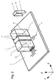
- the Fig. 2 shows an embodiment in which the current to be measured is supplied via an interconnect formed in the printed circuit board 4 to one end of a power strip 16 made of metal and away from the other end of the power strip 16 again.
- the current bar 16 is shown next to the circuit board 4 again, it is U-shaped, ie the current bar 16 consists of three mutually orthogonal sections 17, 18 and 19, wherein the ends of the current bar 16 are formed so that they are on the circuit board 4th can be fixed in contact with the conductor 15.
- the two opposite, extending in the x direction wide outer walls 12 and 13 of the housing 1 are provided with a groove 14 which receives the first portion 17 and the third portion 19 of the power strip 16.
- the depth T of the groove 14 is greater than the thickness D of the current loop 16, so that the current bar 16 does not electrically come into contact with a screen mounted at the end, which serves to shield external magnetic fields.
- the housing 1 can also, as in the Fig. 3 is shown to be provided with two or three or more grooves 14, each groove 14 receives a current bar 16.
- the current bumps 16 are electrically connected in series if the magnetic field generated by the current to be measured at the location of the magnetic field sensor 2 is to be increased.
- the current bars 16 are electrically connected in parallel, if the electrical load and the thermal load caused by the electrical load of the current bar 16 to be reduced. If the current bar 16 side by side not find space, because Its cross section must reach a predetermined minimum size, which is designed for a certain maximum current, the current bar 16 may also be arranged one above the other. This embodiment is in the Fig. 4 shown.
- the current lugs 16 are preferably glued together with electrically non-conductive and thus insulating adhesive together to form a single component.
- the Fig. 5 shows an embodiment in which the current to be measured is supplied via a cable 20.
- the housing 1 with the magnetic field sensor 2 is located at the edge of the circuit board 4 and the circuit board 4 is provided with two outgoing from the edge slots 21 and 22 which extend parallel to the outer walls 12 and 13.
- the cable 20 takes over the functions of the conductor 15 and the / the current bar 16 according to the previous embodiments.
- the cable 20 is inserted into the slot 21 and the slot 22 and the groove 14, so that it encloses the housing 1 in the same manner as a current strap U-shaped.
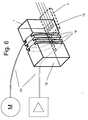
- the Fig. 6 shows an embodiment in which the cable 20 is wound around the housing 1 several times.
- the circuit board 4 serves only as a contacting member between the housing 1 and a connecting cable, which includes the electrical lines to the magnetic field sensor 2.
- the circuit board 4 may be formed as a plug to make a detachable connection with the connection cable can. This solution makes it possible to use the device for measuring current at any location. In the example, it measures the current flowing through a motor M.
- the cable 20 connects the output stage of a control unit to the motor M.
- the cable 20 can be wound around the housing 1 without having to be detached from the control unit or from the motor M.
- the Fig. 7 shows the fully assembled device for current measurement, which consists of the circuit board 4, the housing 1 with the integrated magnetic field sensor 2 and the groove 14, at least one current bar 16 and the cable 20 and a shield 23 for the shielding of an external magnetic field.
- the screen 23 abuts against the outer walls 12 and 13 on both sides of the groove 14. Between the current bar 16 and the screen 23 is a small air gap.
- the depth of the groove 14 is, as explained above, so dimensioned that the contour of the housing 1 acts as a spacer for the screen 23, such that the screen 23 does not come into contact with the current bar 16.
- the screen 23 and the power strip 16 are therefore electrically isolated from each other, without further measures such as the attachment of an insulating layer on the screen 23 or the power strip 16 are required.
- the screen 23 is adhered to the housing 1 and dimensioned so that an air gap remains between the lower edge of the screen 23 and the circuit board 4, which is at least so large that the screen 23 does not come into contact with the electrical terminals of Housing 1 and / or the conductor tracks on the circuit board 4th
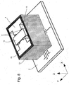
- the Fig. 8 shows a further embodiment of the fully assembled device for current measurement, in which the ends of the outer walls 12 and 13 are formed with a projection acting as a spacer 24.
- the screen 23 abuts against the projections 24 and thus also here - on both sides of the groove 14 - on the outer walls 12 and 13 at. Because here the projections 24 take over the function of a spacer for the screen 23, it is no longer necessary that the depth of the groove 14 is greater than the thickness of the current bar 16.
- the screen 23 has recesses in the region of the electrical connections of the housing 1 and the printed conductors on the printed circuit board 4. During assembly, the screen 23 is placed over the housing 1 until the screen 23 touches the printed circuit board 4.
Landscapes
- Physics & Mathematics (AREA)
- General Physics & Mathematics (AREA)
- Measuring Instrument Details And Bridges, And Automatic Balancing Devices (AREA)
Description
- Die Erfindung betrifft eine Vorrichtung zur Strommessung.
- Stromsensoren, die auf der Messung des von einem Strom erzeugten Magnetfelds basieren, werden immer häufiger und für die verschiedenartigsten Anwendungen eingesetzt. Weit verbreitet ist die als C-shape bekannte Technologie, bei der ein Joch aus ferromagnetischem Material einen Stromleiter mit Ausnahme eines dünnen Luftspalts vollständig umschliesst. Im Luftspalt ist ein Hallelement angeordnet, das das von dem im Stromleiter fliessenden Strom erzeugte und vom Joch verstärkte Magnetfeld misst. Diese Technologie hat mehrere Nachteile. Einerseits sind der Miniaturisierung Grenzen gesetzt. Andererseits ist die Montage der Stromsensoren aufwendig, da der Stromleiter durch das Joch hindurchgeführt werden muss. Aus der
EP 233988 A1 DE 19741417 A1 ist ein Stromsensor mit einem U-förmig gebogenen Stromleiter und einem Hallelement bekannt. Das Hallelement befindet sich auf einer Platine, die senkrecht zu einer zweiten Hauptplatine angeordnet und mit dieser verbunden ist. Ein Schirm schirmt den Stromsensor gegen äussere Magnetfelder ab. Auch diese Lösung ist ziemlich kompliziert. Aus derWO 03/038452 A1 - Aus der
EP 155391 A1 - Aus der
EP 292636 A1 - Der Erfindung liegt die Aufgabe zugrunde, einen Stromsensor für die Messung relativ kleiner Ströme im Bereich von typischerweise 0 bis 10A oder 0 bis 20A zu entwickeln, der wenig Platz beansprucht, kostengünstig herstellbar und einfach einsetzbar ist.
- Die genannte Aufgabe wird erfindungsgemäss gelöst durch die Merkmale des Anspruchs 1. Vorteilhafte Ausgestaltungen ergeben sich aus den abhängigen Ansprüchen.
- Die Erfindung löst die genannte Aufgabe durch einen modularen Aufbau, bei dem die einzelnen Komponenten optimal aufeinander und auf eine Vielzahl von möglichen Anwendungen abgestimmt sind. Die Vorrichtung zur Strommessung ist auf einfache Weise auf eine Leiterplatte integrierbar, wobei die Leiterplatte einen Teil der Vorrichtung bildet. Die Vorrichtung umfasst weiter einen Stromleiter, ein Gehäuse mit einem im Gehäuse angeordneten Magnetfeldsensor für die Messung des Magnetfelds, das von dem durch den Stromleiter fliessenden Strom erzeugt wird, und einen geschlossenen Schirm aus magnetischem Material für die Abschirmung äusserer magnetischer Störfelder. Das Gehäuse wird auf der Leiterplatte montiert, wobei gleichzeitig die elektrischen Verbindungen zwischen dem Magnetfeldsensor und der Leiterplatte hergestellt werden. Der Stromleiter umfasst mindestens einen U-förmigen Strombügel mit drei im wesentlichen orthogonal zueinander verlaufenden Abschnitten. Der Strombügel wird über das Gehäuse gestülpt und auf der Leiterplatte angelötet. Der zu messende Strom wird über einen in die Leiterplatte integrierten Strompfad zum Strombügel zu- und weggeführt. Die drei Abschnitte des U-förmigen Strombügels definieren eine Ebene E. Es ist möglich, mehrere Strombügel nebeneinander oder übereinander anzuordnen, die über entsprechende Strompfade in der Leiterplatte parallel oder seriell verdrahtet sind. Alternativ wird der zu messende Strom über ein Kabel zugeführt, das um das Gehäuse gewickelt wird. Das Kabel übernimmt dabei die Funktion des/der Strombügel. Bei dieser Lösung ist das Gehäuse mit dem Magnetfeldsensor bevorzugt am Rand der Leiterplatte angeordnet und die Leiterplatte mit vom Rand ausgehenden Schlitzen versehen, damit das Kabel auf einfache Weise um das Gehäuse gewickelt werden kann. Der Magnetfeldsensor umfasst einen Halbleiterchip und ist empfindlich auf ein Magnetfeld, das parallel zur aktiven Oberfläche des Halbleiterchips und senkrecht zur Ebene E verläuft. Zwei einander gegenüberliegende Aussenwände des Gehäuses weisen eine Rille auf, die den ersten und den dritten Abschnitt des Strombügels bzw. das Kabel aufnimmt. Der Schirm wird über das Gehäuse gestülpt und liegt an den Aussenwänden beidseitig der Rille an. Die Tiefe der Rille ist so gross bemessen, dass zwischen dem Strombügel und dem Schirm auf jeden Fall ein Luftspalt besteht, so dass der Strombügel und der Schirm elektrisch voneinander getrennt sind, ohne dass weitere Massnahmen wie zum Beispiel eine zusätzliche Isolationsschicht nötig sind. Diese Vorrichtung zeichnet sich durch einen kompakten Aufbau und eine einfache Montage aus. Die einzelnen Komponenten - Gehäuse mit dem Magnetfeldsensor, Strombügel bzw. Kabel, Schirm - werden nacheinander montiert. Weil der Strombügel bzw. das Kabel in eine Rille eingebettet ist und weil der Schirm im Presssitz am Gehäuse anliegt, ergibt sich eine hohe Langzeitstabilität. Weil die aktive Oberfläche des Halbleiterchips senkrecht zu der vom Strombügel aufgespannten Ebene E verläuft, ergibt sich eine schmale Bauform des Gehäuses, die wiederum einen geringen Abstand zwischen den äusseren Abschnitten des Strombügels ermöglicht. Daraus resultiert eine hohe Empfindlichkeit.
- Die Erfindung wird nachfolgend anhand von Ausführungsbeispielen und anhand der Zeichnung näher erläutert.
- Es zeigen:
- Fig. 1
- ein auf einer Leiterplatte befestigtes Gehäuse mit einem Magnetfeldsensor,
- Fig. 2
- die Leiterplatte mit dem Gehäuse und einem über das Gehäuse gestülpten Strombügel,
- Fig. 3
- die Leiterplatte mit dem Gehäuse und mehrere, nebeneinander angeordnete Strombügel,
- Fig. 4
- die Leiterplatte mit dem Gehäuse und mehrere, übereinander angeordnete Strombügel,
- Fig. 5
- die Leiterplatte mit dem Gehäuse und einem einmal um das Gehäuse gewickelten Kabel,
- Fig. 6
- die Leiterplatte mit dem Gehäuse und einem mehrmals um das Gehäuse gewickelten Kabel,
- Fig. 7
- die fertig montierte Vorrichtung zur Strommessung, und
- Fig. 8
- ein weiteres Beispiel der fertig montierten Vorrichtung zur Strommessung.
- In den Figuren sind die Achsen eines kartesischen Koordinatensystems mit x, y und z bezeichnet. Die
Fig. 1 zeigt in perspektivischer und transparenter Darstellung ein Gehäuse 1 mit einem Magnetfeldsensor 2 und einer elektronischen Schaltung für den Betrieb des Magnetfeldsensors 2. Das Gehäuse 1 hat eine relativ flache, im wesentlichen quaderförmige Form. Das Gehäuse 1 ist ausgelegt für eine hochkantige Montage auf einer Leiterplatte 4, d.h. eine schmale Längswand des Gehäuses 1 liegt auf der Leiterplatte 4 auf. - Der Magnetfeldsensor 2 ist empfindlich auf ein in x-Richtung gerichtetes Magnetfeld. Die elektronische Schaltung umfasst einen Halbleiterchip 5 mit integrierten Schaltungen, sowie fakultativ separate elektronische Bauteile 6 wie zum Beispiel Schutzkondensatoren. Es sind verschiedene Typen von Magnetfeldsensoren geeignet. Der in der
Fig. 1 dargestellte Magnetfeldsensor 2 umfasst zwei durch einen Luftspalt 7 getrennte Magnetfeldkonzentratoren 8 und 9 und ein Hallelement 10. Die Magnetfeldkonzentratoren 8 und 9 sind auf der aktiven Oberfläche des Halbleiterchips 5 angeordnet. Das Hallelement 10 ist im Halbleiterchip 5 integriert und befindet sich im Bereich des Luftspalts 7 zwischen den Magnetfeldkonzentratoren 8 und 9, wobei vom einen Magnetfeldkonzentrator 8 ausgehende Feldlinien des Magnetfelds das Hallelement 10 durchfluten und auf den anderen Magnetfeldkonzentrator 9 auftreffen. Aus derEP 772046 - Der Magnetfeldsensor 2 soll im wesentlichen nur empfindlich sein auf die x-Komponente eines äusseren Magnetfelds und unempfindlich auf die y- und z-Komponente des äusseren Magnetfelds. Der oben beschriebene Magnetfeldsensor 2 mit den beiden Magnetfeldkonzentratoren 8, 9 und dem Hallelement 10 erfüllt diese Anforderungen in hohem Masse. Der Magnetfeldsensor 2 kann aber auch ein anderer Sensor sein, der diese Anforderung erfüllt, z. B. ein AMR (anisotropic magnetic resistance) oder GMR (giant magnetic resistance) Sensor. Diese Sensoren umfassen ein ferromagnetisches Widerstandselement, dessen elektrischer Widerstand von der Stärke des Magnetfelds abhängt. Der Magnetfeldsensor 2 kann des weiteren auch ein Fluxgate Sensor sein. Ein Fluxgate Sensor umfasst einen ferromagnetischen Kern. Das ferromagnetische Widerstandselement bzw. der ferromagnetische Kern ist auf der aktiven Oberfläche des Halbleiterchips 5 angeordnet und beeinflusst den Verlauf der magnetischen Feldlinien in ähnlicher Weise wie die Magnetfeldkonzentratoren 8 und 9 beim vorhergehenden Beispiel.
- Im Beispiel ist das Gehäuse 1 in der als MID (molded interconnect device) bekannten Technologie gefertigt. Bei dieser Technologie werden im Spritzgussverfahren nacheinander ein metallisierbarer und ein nicht-metallisierbarer Kunststoff abgespritzt, wobei ein dreidimensionales Gehäuseunterteil entsteht. Anschliessend wird das Gehäuseunterteil für die Bildung von Leiterbahnen 11 metallisiert und bei Bedarf galvanisch verstärkt. Nach der Montage und elektrischen Verdrahtung des Magnetfeldsensors 2 mit den Leiterbahnen 11 im Gehäuseunterteil und der Montage der elektronischen Bauteile 6 wird das Gehäuseunterteil beispielsweise durch Vergiessen mit einem Kunststoff zum vollständigen Gehäuse 1 komplettiert. Die Leiterbahnen 11 enden auf einer Schmalseite des Gehäuses 1 als SMD Kontakte, so dass das Gehäuse 1 in der SMD (surface mount device) Technologie auf der Leiterplatte 4 befestigt werden kann. Vorteilhafterweise ist wenigstens die Fläche des Gehäuses 1, auf der der Halbleiterchip 5 aufliegt, metallisiert, um eine elektrische Abschirmungswirkung zu erzielen. Die MID Technologie bietet eine zweite Metallisierungsebene, die vorteilhafterweise für die Erzielung einer optimalen elektrischen Abschirmung benützt und entsprechend ausgestaltet wird.
- Alternativ ist das Gehäuse 1 in einer herkömmlichen IC Technologie gefertigt, bei der der Halbleiterchip 5 auf einem sogenannten Leadframe montiert, verdrahtet und mit Kunststoff verkapselt wird, wobei der elektrische Kontakt mit der Leiterplatte 4 über elektrische Anschlussbeine erfolgt, die aus einer Schmalseite des Gehäuses 1 herausragen. Die Leiterplatte 4 kann z. B. Durchkontaktierungen für die Anschlussbeine des Gehäuses 1 aufweisen.
- Die
Fig. 2 zeigt ein Ausführungsbeispiel, bei dem der zu messende Strom über eine in der Leiterplatte 4 gebildete Leiterbahn 15 einem Ende eines Strombügels 16 aus Metall zugeführt und vom anderen Ende des Strombügels 16 wieder weggeführt wird. Der Strombügel 16 ist neben der Leiterplatte 4 nochmals dargestellt, er ist U-förmig, d.h. der Strombügel 16 besteht aus drei orthogonal zueinander verlaufenden Abschnitten 17, 18 und 19, wobei die Enden des Strombügels 16 so ausgebildet sind, dass sie auf der Leiterplatte 4 in Kontakt mit der Leiterbahn 15 befestigt werden können. Die beiden einander gegenüberliegenden, in x-Richtung verlaufenden breiten Aussenwände 12 und 13 des Gehäuses 1 sind mit einer Rille 14 versehen, die den ersten Abschnitt 17 und den dritten Abschnitt 19 des Strombügels 16 aufnimmt. Die Tiefe T der Rille 14 ist grösser als die Dicke D des Strombügels 16, so dass der Strombügel 16 elektrisch nicht in Kontakt kommt mit einem am Schluss montierten Schirm, der zur Abschirmung äusserer Magnetfelder dient. - Das Gehäuse 1 kann auch, wie in der
Fig. 3 gezeigt ist, mit zwei oder drei oder noch mehr Rillen 14 versehen sein, wobei jede Rille 14 einen Strombügel 16 aufnimmt. Die Strombügel 16 sind elektrisch in Reihe geschaltet, falls das von dem zu messenden Strom erzeugte Magnetfeld am Ort des Magnetfeldsensors 2 erhöht werden soll. Alternativ sind die Strombügel 16 elektrisch parallel geschaltet, falls die elektrische Belastung und die durch die elektrische Belastung verursachte thermische Belastung des Strombügels 16 verkleinert werden soll. Falls die Strombügel 16 nebeneinander nicht Platz finden, weil ihr Querschnitt eine vorbestimmte Mindestgrösse erreichen muss, die für eine bestimmte maximale Stromstärke ausgelegt ist, können die Strombügel 16 auch übereinander angeordnet sein. Dieses Ausführungsbeispiel ist in derFig. 4 gezeigt. Die Strombügel 16 sind bevorzugt mit elektrisch nicht leitendem und somit isolierendem Klebstoff miteinander zu einem einzigen Bauteil verklebt. - Die
Fig. 5 zeigt ein Ausführungsbeispiel, bei dem der zu messende Strom über ein Kabel 20 zugeführt wird. Das Gehäuse 1 mit dem Magnetfeldsensor 2 befindet sich am Rand der Leiterplatte 4 und die Leiterplatte 4 ist mit zwei vom Rand ausgehenden Schlitzen 21 und 22 versehen, die parallel zu den Aussenwänden 12 und 13 verlaufen. Das Kabel 20 übernimmt die Funktionen der Leiterbahn 15 und des/der Strombügel 16 gemäss den vorherigen Ausführungsbeispielen. Das Kabel 20 wird in den Schlitz 21 und den Schlitz 22 und die Rille 14 hineingelegt, so dass es das Gehäuse 1 in gleicher Art wie ein Strombügel U-förmig umschliesst. DieFig. 6 zeigt ein Ausführungsbeispiel, bei dem das Kabel 20 mehrmals um das Gehäuse 1 herum gewickelt ist. Die Leiterplatte 4 dient hier nur als Kontaktierungsglied zwischen dem Gehäuse 1 und einem Anschlusskabel, das die elektrischen Leitungen zum Magnetfeldsensor 2 beinhaltet. Die Leiterplatte 4 kann als Stecker ausgebildet sein, um eine lösbare Verbindung mit dem Anschlusskabel herstellen zu können. Diese Lösung erlaubt es, die Vorrichtung zur Strommessung an einem beliebigen Ort einzusetzen. Im Beispiel misst sie den Strom, der durch einen Motor M fliesst. Das Kabel 20 verbindet die Ausgangsstufe einer Steuereinheit mit dem Motor M. Das Kabel 20 kann um das Gehäuse 1 gewickelt werden, ohne dass es von der Steuereinheit oder vom Motor M gelöst werden muss. - Die
Fig. 7 zeigt die fertig montierte Vorrichtung zur Strommessung, die aus der Leiterplatte 4, dem Gehäuse 1 mit dem integrierten Magnetfeldsensor 2 und der Rille 14, mindestens einem Strombügel 16 bzw. dem Kabel 20 und einem Schirm 23 für die Abschirmung eines äusseren Magnetfelds besteht. Der Schirm 23 liegt an den Aussenwänden 12 und 13 auf beiden Seiten der Rille 14 an. Zwischen dem Strombügel 16 und dem Schirm 23 befindet sich ein kleiner Luftspalt. Die Tiefe der Rille 14 ist wie bereits weiter oben erläutert so bemessen, dass die Kontur des Gehäuses 1 als Abstandshalter für den Schirm 23 wirkt, derart, dass der Schirm 23 nicht in Kontakt kommt mit dem Strombügel 16. Der Schirm 23 und der Strombügel 16 sind also elektrisch voneinander getrennt, ohne dass weitere Massnahmen wie zum Beispiel das Anbringen einer Isolationsschicht auf den Schirm 23 oder den Strombügel 16 erforderlich sind. Bei diesem Beispiel ist der Schirm 23 am Gehäuse 1 angeklebt und so bemessen, dass ein Luftspalt zwischen dem unteren Rand des Schirms 23 und der Leiterplatte 4 verbleibt, der mindestens so gross ist, dass der Schirm 23 nicht in Kontakt kommt mit den elektrischen Anschlüssen des Gehäuses 1 und/oder den Leiterbahnen auf der Leiterplatte 4. - Die
Fig. 8 zeigt ein weiteres Ausführungsbeispiel der fertig montierten Vorrichtung zur Strommessung, bei dem die Enden der Aussenwände 12 und 13 mit einem als Distanzgeber wirkenden Vorsprung 24 ausgebildet sind. Der Schirm 23 liegt an den Vorsprüngen 24 an und somit auch hier - beidseits der Rille 14 - an den Aussenwänden 12 und 13 an. Weil hier die Vorsprünge 24 die Funktion als Abstandshalter für den Schirm 23 übernehmen, ist es nicht mehr erforderlich, dass die Tiefe der Rille 14 grösser als die Dicke des Strombügels 16 ist. Bei diesem Beispiel weist der Schirm 23 Ausnehmungen auf im Bereich der elektrischen Anschlüsse des Gehäuses 1 und der Leiterbahnen auf der Leiterplatte 4. Bei der Montage wird der Schirm 23 über das Gehäuse 1 gestülpt, bis der Schirm 23 die Leiterplatte 4 berührt.
Claims (4)
- Vorrichtung zur Strommessung, umfassend
eine Leiterplatte (4),
einen Stromleiter, durch den der zu messende Strom fliesst,
ein Gehäuse (1) mit einem im Gehäuse (1) angeordneten Magnetfeldsensor (2) für die Messung des Magnetfelds, das von dem durch den Stromleiter fliessenden Strom erzeugt wird, und
eine Abschirmung für die Abschirmung äusserer Magnetfelder, dadurch gekennzeichnet, dass das Gehäuse (1) eine flache, quaderförmige Form hat und derart auf der Leiterplatte (4) montiert ist, dass eine schmale Längswand auf der Leiterplatte (4) aufliegt, wobei der elektrische Kontakt mit der Leiterplatte (4) über an der schmalen Längswand des Gehäuses (1) angeordnete SMD Kontakte oder über elektrische Anschlussbeine erfolgt, die aus der schmalen Längswand des Gehäuses (1) herausragen,
dass zwei einander gegenüberliegende Aussenwände (12, 13) des Gehäuses (1) eine Rille (14) aufweisen, die eine Ebene E definiert,
dass der Stromleiter einen U-förmigen, auf der Leiterplatte (4) angelöteten Strombügel (16) mit drei im wesentlichen orthogonal zueinander verlaufenden Abschnitten (17, 18, 19) und eine in der Leiterplatte (4) angebrachte Leiterbahn (15) umfasst oder dass der Stromleiter ein Kabel (20) ist, wobei die Rille (14) den ersten und den dritten Abschnitt des Strombügels (16) bzw. das Kabel (20) aufnimmt,
dass der Magnetfeldsensor (2) einen Halbleiterchip umfasst, der sich in einer senkrecht zur Leiterplatte (4) verlaufenden Ebene erstreckt, und empfindlich ist auf ein Magnetfeld, das parallel zur aktiven Oberfläche des Halbleiterchips und senkrecht zur Ebene E verläuft,
dass die Abschirmung ein geschlossener Schirm (23) aus magnetischem Material ist, der auf beiden Seiten der Rille (14) an den besagten Aussenwänden (12, 13) anliegt, und dass im Fall der Ausführung mit dem Strombügel (16) die Tiefe der Rille (14) grösser als die Dicke des Strömbügels (16) oder das Gehäuse (1) mit Vorsprüngen (24) ausgebildet ist, so dass der Strombügel (16) elektrisch nicht in Kontakt kommt mit dem Schirm (23). - Vorrichtung nach Anspruch 1, dadurch gekennzeichnet, dass das Gehäuse (1) auf einer Aussenwand endende Leiterbahnen (11) aufweist.
- Vorrichtung nach Anspruch 2, dadurch gekennzeichnet, dass der Magnetfeldsensor (2) ein im Halbleiterchip (5) integriertes Hallelement (10) und mindestens einen auf dem Halbleiterchip (5) angebrachten Magnetfeldkonzentrator (12, 13) umfasst.
- Vorrichtung nach Anspruch 1 oder 2, dadurch gekennzeichnet, dass der Magnetfeldsensor (2) ein AMR oder GMR oder Fluxgate Sensor ist.
Applications Claiming Priority (1)
| Application Number | Priority Date | Filing Date | Title |
|---|---|---|---|
| CH8102006A CH698504B1 (de) | 2006-05-16 | 2006-05-16 | Vorrichtung zur Strommessung. |
Publications (4)
| Publication Number | Publication Date |
|---|---|
| EP1857823A2 EP1857823A2 (de) | 2007-11-21 |
| EP1857823A3 EP1857823A3 (de) | 2013-07-10 |
| EP1857823B1 true EP1857823B1 (de) | 2014-10-15 |
| EP1857823B8 EP1857823B8 (de) | 2015-01-07 |
Family
ID=38461146
Family Applications (1)
| Application Number | Title | Priority Date | Filing Date |
|---|---|---|---|
| EP20070107590 Not-in-force EP1857823B8 (de) | 2006-05-16 | 2007-05-07 | Vorrichtung zur Strommessung |
Country Status (2)
| Country | Link |
|---|---|
| EP (1) | EP1857823B8 (de) |
| CH (1) | CH698504B1 (de) |
Families Citing this family (7)
| Publication number | Priority date | Publication date | Assignee | Title |
|---|---|---|---|---|
| CH705027A1 (de) | 2011-05-30 | 2012-11-30 | Melexis Technologies Nv | Vorrichtung zur Messung eines durch ein elektrisches Kabel fliessenden Stroms. |
| JP6032534B2 (ja) * | 2012-07-13 | 2016-11-30 | 甲神電機株式会社 | 磁気シールド及びこれを備えた電流検出器 |
| DE102018120008B4 (de) * | 2018-08-16 | 2023-08-10 | Phoenix Contact Gmbh & Co. Kg | Strommessgerät zum Erfassen von Strömen in elektrischen Leitungen |
| CN112578174B (zh) * | 2019-09-30 | 2023-04-07 | 比亚迪半导体股份有限公司 | 电流传感器 |
| DE102019132593B4 (de) * | 2019-12-02 | 2021-07-22 | Schaeffler Technologies AG & Co. KG | Stromsensor |
| WO2024177013A1 (ja) * | 2023-02-20 | 2024-08-29 | 旭化成エレクトロニクス株式会社 | 半導体パッケージ、及びモジュール |
| CN119414070B (zh) * | 2024-12-16 | 2025-09-16 | 珠海多创科技有限公司 | 一种电流传感器及电子设备 |
Family Cites Families (5)
| Publication number | Priority date | Publication date | Assignee | Title |
|---|---|---|---|---|
| DE3479758D1 (en) | 1984-01-07 | 1989-10-19 | Duerrwaechter E Dr Doduco | Device for measuring electrical currents using a magnetic-field sensor |
| CH670004A5 (de) | 1986-02-10 | 1989-04-28 | Landis & Gyr Ag | |
| EP0292636A1 (de) | 1987-05-26 | 1988-11-30 | Landis & Gyr Betriebs AG | Messwandler zum Messen des in einem elektrischen Leiter fliessenden Stromes |
| DE19741417B4 (de) | 1997-09-19 | 2004-02-26 | Klaus Bruchmann | Strommessgerät mit Hallsensor |
| CN1295514C (zh) | 2001-11-01 | 2007-01-17 | 旭化成电子材料元件株式会社 | 电流传感器与电流传感器的制造方法 |
-
2006
- 2006-05-16 CH CH8102006A patent/CH698504B1/de not_active IP Right Cessation
-
2007
- 2007-05-07 EP EP20070107590 patent/EP1857823B8/de not_active Not-in-force
Also Published As
| Publication number | Publication date |
|---|---|
| EP1857823B8 (de) | 2015-01-07 |
| EP1857823A3 (de) | 2013-07-10 |
| EP1857823A2 (de) | 2007-11-21 |
| CH698504B1 (de) | 2009-08-31 |
Similar Documents
| Publication | Publication Date | Title |
|---|---|---|
| EP1857823B1 (de) | Vorrichtung zur Strommessung | |
| EP2437072B1 (de) | Stromsensor | |
| EP2530475B1 (de) | Vorrichtung zur Messung eines durch ein elektrisches Kabel fliessenden Stroms | |
| EP2801832B1 (de) | Vorrichtung zur Strommessung | |
| DE19680088B4 (de) | Kalibrier- und Herstellungsverfahren für einen Magnetsensor | |
| DE102008039568B4 (de) | Stromerfassungsvorrichtung | |
| DE602005003777T2 (de) | Oberflächenmontierter integrierter Stromsensor | |
| DE10041599B4 (de) | Stromsensor und elektrischer Schaltkreis, der diesen benutzt | |
| DE19680089B4 (de) | Magnetsensor mit verbesserter Kalibrierbarkeit | |
| DE60027257T2 (de) | Stromdetektor mit einer Hall-Effekt-Anordnung | |
| DE69532396T2 (de) | Magnetfeldmessgerät | |
| DE10045563B4 (de) | Leistungshalbleiter-Modulbaugruppe | |
| WO2014001473A1 (de) | Anordnung zur strommessung | |
| DE112016002481T5 (de) | Stromsensor | |
| EP1772737A2 (de) | Baugruppe zur Strommessung | |
| WO2011023495A1 (de) | Magnetfeldsensor | |
| DE102022101970B4 (de) | Magnetkernfreies Stromsensormodul | |
| EP0637081B1 (de) | Mikrosensor mit Steckeranschluss | |
| EP0188789B1 (de) | Magnetfeldsensor | |
| DE102016216330A1 (de) | Flexible Spulenordnung für einen magnetoelektrischen Weggeber, Weggeber und Herstellungsverfahren | |
| EP0675368A1 (de) | Eingangsteil eines Messgerätes | |
| DE19544660A1 (de) | Steckeranordnung für ein elektrisches Gerät | |
| DE4211486C1 (de) | ||
| CH693656A5 (de) | Isolationskamm für Multikontaktstecker. | |
| DE112021002950T5 (de) | Stromsensor |
Legal Events
| Date | Code | Title | Description |
|---|---|---|---|
| PUAI | Public reference made under article 153(3) epc to a published international application that has entered the european phase |
Free format text: ORIGINAL CODE: 0009012 |
|
| AK | Designated contracting states |
Kind code of ref document: A2 Designated state(s): AT BE BG CH CY CZ DE DK EE ES FI FR GB GR HU IE IS IT LI LT LU LV MC MT NL PL PT RO SE SI SK TR |
|
| AX | Request for extension of the european patent |
Extension state: AL BA HR MK YU |
|
| RAP1 | Party data changed (applicant data changed or rights of an application transferred) |
Owner name: MELEXIS TESSENDERLO NV Owner name: HARTING MITRONICS AG |
|
| PUAL | Search report despatched |
Free format text: ORIGINAL CODE: 0009013 |
|
| RAP1 | Party data changed (applicant data changed or rights of an application transferred) |
Owner name: MELEXIS TECHNOLOGIES NV Owner name: HARTING MITRONICS AG |
|
| AK | Designated contracting states |
Kind code of ref document: A3 Designated state(s): AT BE BG CH CY CZ DE DK EE ES FI FR GB GR HU IE IS IT LI LT LU LV MC MT NL PL PT RO SE SI SK TR |
|
| AX | Request for extension of the european patent |
Extension state: AL BA HR MK RS |
|
| RIC1 | Information provided on ipc code assigned before grant |
Ipc: G01R 15/20 20060101AFI20130531BHEP |
|
| RAP1 | Party data changed (applicant data changed or rights of an application transferred) |
Owner name: HARTING AG Owner name: MELEXIS TECHNOLOGIES NV |
|
| 17P | Request for examination filed |
Effective date: 20140110 |
|
| RBV | Designated contracting states (corrected) |
Designated state(s): AT BE BG CH CY CZ DE DK EE ES FI FR GB GR HU IE IS IT LI LT LU LV MC MT NL PL PT RO SE SI SK TR |
|
| GRAP | Despatch of communication of intention to grant a patent |
Free format text: ORIGINAL CODE: EPIDOSNIGR1 |
|
| AKX | Designation fees paid |
Designated state(s): CH DE FR GB IT LI |
|
| INTG | Intention to grant announced |
Effective date: 20140228 |
|
| GRAS | Grant fee paid |
Free format text: ORIGINAL CODE: EPIDOSNIGR3 |
|
| RBV | Designated contracting states (corrected) |
Designated state(s): BE CH DE FR GB IT LI |
|
| RAP1 | Party data changed (applicant data changed or rights of an application transferred) |
Owner name: MELEXIS TECHNOLOGIES NV |
|
| RAP1 | Party data changed (applicant data changed or rights of an application transferred) |
Owner name: MELEXIS TECHNOLOGIES NV |
|
| GRAA | (expected) grant |
Free format text: ORIGINAL CODE: 0009210 |
|
| AK | Designated contracting states |
Kind code of ref document: B1 Designated state(s): BE CH DE FR GB IT LI |
|
| REG | Reference to a national code |
Ref country code: GB Ref legal event code: FG4D Free format text: NOT ENGLISH Ref country code: CH Ref legal event code: EP |
|
| RAP2 | Party data changed (patent owner data changed or rights of a patent transferred) |
Owner name: MELEXIS TECHNOLOGIES NV |
|
| REG | Reference to a national code |
Ref country code: DE Ref legal event code: R096 Ref document number: 502007013514 Country of ref document: DE Effective date: 20141120 |
|
| RAP2 | Party data changed (patent owner data changed or rights of a patent transferred) |
Owner name: MELEXIS TECHNOLOGIES NV |
|
| REG | Reference to a national code |
Ref country code: CH Ref legal event code: NV Representative=s name: PATENTANWALTSBUERO DR. URS FALK, CH |
|
| REG | Reference to a national code |
Ref country code: DE Ref legal event code: R097 Ref document number: 502007013514 Country of ref document: DE |
|
| PLBE | No opposition filed within time limit |
Free format text: ORIGINAL CODE: 0009261 |
|
| STAA | Information on the status of an ep patent application or granted ep patent |
Free format text: STATUS: NO OPPOSITION FILED WITHIN TIME LIMIT |
|
| PG25 | Lapsed in a contracting state [announced via postgrant information from national office to epo] |
Ref country code: IT Free format text: LAPSE BECAUSE OF FAILURE TO SUBMIT A TRANSLATION OF THE DESCRIPTION OR TO PAY THE FEE WITHIN THE PRESCRIBED TIME-LIMIT Effective date: 20141015 |
|
| 26N | No opposition filed |
Effective date: 20150716 |
|
| GBPC | Gb: european patent ceased through non-payment of renewal fee |
Effective date: 20150507 |
|
| REG | Reference to a national code |
Ref country code: FR Ref legal event code: ST Effective date: 20160129 |
|
| PG25 | Lapsed in a contracting state [announced via postgrant information from national office to epo] |
Ref country code: GB Free format text: LAPSE BECAUSE OF NON-PAYMENT OF DUE FEES Effective date: 20150507 |
|
| PG25 | Lapsed in a contracting state [announced via postgrant information from national office to epo] |
Ref country code: FR Free format text: LAPSE BECAUSE OF NON-PAYMENT OF DUE FEES Effective date: 20150601 |
|
| PGFP | Annual fee paid to national office [announced via postgrant information from national office to epo] |
Ref country code: CH Payment date: 20170621 Year of fee payment: 11 Ref country code: DE Payment date: 20170529 Year of fee payment: 11 |
|
| PGFP | Annual fee paid to national office [announced via postgrant information from national office to epo] |
Ref country code: BE Payment date: 20170518 Year of fee payment: 11 |
|
| REG | Reference to a national code |
Ref country code: DE Ref legal event code: R119 Ref document number: 502007013514 Country of ref document: DE |
|
| REG | Reference to a national code |
Ref country code: CH Ref legal event code: PL |
|
| REG | Reference to a national code |
Ref country code: BE Ref legal event code: MM Effective date: 20180531 |
|
| PG25 | Lapsed in a contracting state [announced via postgrant information from national office to epo] |
Ref country code: LI Free format text: LAPSE BECAUSE OF NON-PAYMENT OF DUE FEES Effective date: 20180531 Ref country code: CH Free format text: LAPSE BECAUSE OF NON-PAYMENT OF DUE FEES Effective date: 20180531 |
|
| PG25 | Lapsed in a contracting state [announced via postgrant information from national office to epo] |
Ref country code: DE Free format text: LAPSE BECAUSE OF NON-PAYMENT OF DUE FEES Effective date: 20181201 |
|
| PG25 | Lapsed in a contracting state [announced via postgrant information from national office to epo] |
Ref country code: BE Free format text: LAPSE BECAUSE OF NON-PAYMENT OF DUE FEES Effective date: 20180531 |