EP2801832B1 - Vorrichtung zur Strommessung - Google Patents
Vorrichtung zur Strommessung Download PDFInfo
- Publication number
- EP2801832B1 EP2801832B1 EP14155684.5A EP14155684A EP2801832B1 EP 2801832 B1 EP2801832 B1 EP 2801832B1 EP 14155684 A EP14155684 A EP 14155684A EP 2801832 B1 EP2801832 B1 EP 2801832B1
- Authority
- EP
- European Patent Office
- Prior art keywords
- current
- magnetic field
- current conductor
- conductor
- sensor
- Prior art date
- Legal status (The legal status is an assumption and is not a legal conclusion. Google has not performed a legal analysis and makes no representation as to the accuracy of the status listed.)
- Active
Links
Images
Classifications
-
- G—PHYSICS
- G01—MEASURING; TESTING
- G01R—MEASURING ELECTRIC VARIABLES; MEASURING MAGNETIC VARIABLES
- G01R19/00—Arrangements for measuring currents or voltages or for indicating presence or sign thereof
- G01R19/0092—Measuring current only
-
- G—PHYSICS
- G01—MEASURING; TESTING
- G01R—MEASURING ELECTRIC VARIABLES; MEASURING MAGNETIC VARIABLES
- G01R15/00—Details of measuring arrangements of the types provided for in groups G01R17/00 - G01R29/00, G01R33/00 - G01R33/26 or G01R35/00
- G01R15/14—Adaptations providing voltage or current isolation, e.g. for high-voltage or high-current networks
- G01R15/20—Adaptations providing voltage or current isolation, e.g. for high-voltage or high-current networks using galvano-magnetic devices, e.g. Hall-effect devices, i.e. measuring a magnetic field via the interaction between a current and a magnetic field, e.g. magneto resistive or Hall effect devices
-
- G—PHYSICS
- G01—MEASURING; TESTING
- G01R—MEASURING ELECTRIC VARIABLES; MEASURING MAGNETIC VARIABLES
- G01R33/00—Arrangements or instruments for measuring magnetic variables
- G01R33/02—Measuring direction or magnitude of magnetic fields or magnetic flux
- G01R33/06—Measuring direction or magnitude of magnetic fields or magnetic flux using galvano-magnetic devices
- G01R33/07—Hall effect devices
-
- G—PHYSICS
- G01—MEASURING; TESTING
- G01R—MEASURING ELECTRIC VARIABLES; MEASURING MAGNETIC VARIABLES
- G01R15/00—Details of measuring arrangements of the types provided for in groups G01R17/00 - G01R29/00, G01R33/00 - G01R33/26 or G01R35/00
- G01R15/14—Adaptations providing voltage or current isolation, e.g. for high-voltage or high-current networks
- G01R15/20—Adaptations providing voltage or current isolation, e.g. for high-voltage or high-current networks using galvano-magnetic devices, e.g. Hall-effect devices, i.e. measuring a magnetic field via the interaction between a current and a magnetic field, e.g. magneto resistive or Hall effect devices
- G01R15/207—Constructional details independent of the type of device used
-
- H—ELECTRICITY
- H10—SEMICONDUCTOR DEVICES; ELECTRIC SOLID-STATE DEVICES NOT OTHERWISE PROVIDED FOR
- H10W—GENERIC PACKAGES, INTERCONNECTIONS, CONNECTORS OR OTHER CONSTRUCTIONAL DETAILS OF DEVICES COVERED BY CLASS H10
- H10W74/00—Encapsulations, e.g. protective coatings
-
- H—ELECTRICITY
- H10—SEMICONDUCTOR DEVICES; ELECTRIC SOLID-STATE DEVICES NOT OTHERWISE PROVIDED FOR
- H10W—GENERIC PACKAGES, INTERCONNECTIONS, CONNECTORS OR OTHER CONSTRUCTIONAL DETAILS OF DEVICES COVERED BY CLASS H10
- H10W90/00—Package configurations
- H10W90/701—Package configurations characterised by the relative positions of pads or connectors relative to package parts
- H10W90/751—Package configurations characterised by the relative positions of pads or connectors relative to package parts of bond wires
- H10W90/756—Package configurations characterised by the relative positions of pads or connectors relative to package parts of bond wires between a chip and a stacked lead frame, conducting package substrate or heat sink
Definitions
- the invention relates to a device for measuring current.
- Current sensors are available in many designs and variants.
- Current sensors which detect the magnetic field generated by the current, are packaged in a conventional IC housing and in which the current conductor through which the current to be measured flows is guided through the housing, are known, for example EP 1443332 , WO 2005026749 , WO 2006130393 , DE 102009054892 , US 2004/155644 and CH 703903 .
- Such current sensors contain a current conductor, which is designed as part of a leadframe, which is used for the assembly and production of the electrical connections, and a semiconductor chip mounted on the leadframe, which has at least one magnetic field sensor and for its operation and the processing of its output signal has the necessary electronics.
- current sensors packaged in a conventional IC housing are also known, for example from JP 2003302428 , which are mounted on a circuit board above a conductor track and measure the current flowing through the conductor track.
- Another class of current sensors includes a U-shaped current conductor (bus bar) and an IC housing that can be fitted into it and in which a magnetic field detector is packaged.
- a magnetic field detector is packaged.
- An example of this is the published registration US 2007200551 A1 (Muraki Hitoshi et al) August 12, 2004 . In these current sensors, the magnetic field detector is positioned precisely and stably relative to an upper and parallel lower current-carrying segment of the current conductor.
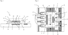
- the Fig. 1 and 2 show in cross section and top view an exemplary embodiment of a device 1 according to the invention for measuring current.
- the device 1 comprises a substrate 2 with a first current conductor 3 and a current sensor 4 with a second current conductor 5.
- the current sensor 4 is packed in an IC housing 6, for example in an SOIC-8 or SOIC-16 housing, and above the first current conductor 3 mounted on the substrate 2.
- the current sensor 4 includes the second Current conductor 5 with molded first and second electrical connecting legs 7 and 8, through which the current to be measured is supplied and removed, and third electrical connecting legs 9, as well as a semiconductor chip 10, which is mounted on the second current conductor 5 on the side facing the substrate 2 is.
- the semiconductor chip 10 has an active surface with a magnetic field sensor 11 and electronic circuits for operating the magnetic field sensor.
- the first and second Connecting legs 7 and 8 protrude from the housing 6 on a first side wall 12 of the housing 6 and the third connecting legs 9 on a side wall 13 of the housing 6 opposite the first side wall 12 and are bent towards the substrate 2. Electrical connections of the semiconductor chip 10 are connected to the third connecting legs 9 via bonding wires 14.
- the current sensor 4 is aligned and mounted on the substrate 2 in such a way that the first current conductor 3 and the second current conductor 5 run parallel to one another and essentially lie one above the other at a distance from one another.
- the two current conductors 3 and 5 are electrically connected to one another in such a way that the current to be measured flows in opposite directions in the two current conductors 3 and 5.
- the magnetic field sensor is sensitive to that component of the magnetic field that runs parallel to the active surface of the semiconductor chip 10, and thus also parallel to the surface of the substrate 2, and perpendicular to the two current conductors 3 and 5.
- the substrate 2 has several conductor tracks which serve to guide the current to be measured to the current sensor 4 and through the first current conductor 3, to supply the current sensor 4 with electrical energy and to direct the output signal of the current sensor 4 to a suitable location.
- the first current conductor 3 is part of such a conductor track 15, which is additionally shaped so that the connecting legs 8 contact the conductor track 15.
- the current to be measured is led through a conductor track 16 to the first connecting legs 7, flows through the second current conductor 5 in the current sensor 4 and then through the connecting legs 8 to the conductor track 15 and through the first current conductor 3.
- the magnetic field that is at the location of the magnetic field sensor is generated when the current flows through the first current conductor 3, and the magnetic field that is generated at the location of the magnetic field sensor when the current flows through the second current conductor 5 point in the same direction and thus add up.
- the magnetic field sensor is preferably a magnetic field sensor as shown in the EP 772046 is known.
- a magnetic field sensor comprises two magnetic field concentrators 17, which are separated by a narrow gap, and two horizontal Hall elements 18 (or clusters of Hall elements), which are arranged on both sides of the gap below the edge of the magnetic field concentrators 17, or a vertical Hall element which is in the gap between the magnetic field concentrators 17 is arranged.
- the magnetic field sensor can also be an AMR (anisotropic magnetoresistive sensor) or a GMR (giant magnetoresistive sensor) or a fluxgate sensor or another magnetic sensor.
- the device according to the invention for measuring current is characterized in that the current to be measured flows firstly through a current conductor, which is part of a current sensor, and secondly through a current conductor which is arranged below the current sensor, the two current conductors running parallel to one another.
- the magnetic field generated by the current to be measured is thereby increased at the location of the magnetic field sensor.
- At least one further power conductor 19 which runs parallel to the first power conductor 3 and is arranged next to or below the first power conductor 3.
- the at least one further current conductor 19 is connected in series with the first current conductor 3 in such a way that the current to be measured flows in the same direction through the first current conductor 3 and the at least one further current conductor 19.
- the connections required for this are guided around the current sensor 4 in such a way that they generate no or a comparatively very small magnetic field at the location of the magnetic field sensor 11.
- the substrate 2 is in particular a circuit board.
- circuit boards often have several levels of metallization.
- the at least one further current conductor 19 and the first current conductor 3 are connected in series and connected to one another by conductor tracks 20 in such a way that the current to be measured flows in the same direction in the first current conductor 3 and in all other current conductors 19.
- the first power conductor 3 and the further power conductors 19 form a coil.
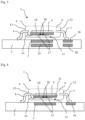
- Such a device for measuring current is shown in cross section Fig. 3 shown.
- the Fig. 4 shows in cross section a device 1 according to the invention for measuring current, in which a ceramic plate 21 is arranged between the semiconductor chip 10 and the second current conductor 5 of the current sensor 4, which serves as an electrical insulator.
- the ceramic plate 21 projects beyond the semiconductor chip 10 on all four sides by at least 0.1 mm, preferably by at least 0.4 mm.
- the thickness of the ceramic plate 21 is typically 0.4 mm or more. In this way, a high voltage strength is achieved between the semiconductor chip 10 and the second current conductor 5.
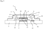
- a magnetic shield 22 can optionally be attached to the side of the second current conductor 5 opposite the semiconductor chip 10. Such an embodiment is in the Fig. 5 shown.
- the magnetic shield 22 serves to shield the magnetic field sensor 11 against a magnetic field that runs parallel to the surface of the semiconductor chip 10, and thus also parallel to the surface of the substrate 2, and perpendicular to the two current conductors 3 and 5.
- the shield 22 can be integrated into the housing 6 of the current sensor 4 or be a separate, ferromagnetic component.
Landscapes
- Physics & Mathematics (AREA)
- General Physics & Mathematics (AREA)
- Condensed Matter Physics & Semiconductors (AREA)
- Measuring Instrument Details And Bridges, And Automatic Balancing Devices (AREA)
Description
- Die Erfindung betrifft eine Vorrichtung zur Strommessung.
- Stromsensoren gibt es in vielen Ausführungen und Varianten. Stromsensoren, die das vom Strom erzeugte Magnetfeld erfassen, in einem herkömmlichen IC Gehäuse verpackt sind und bei denen der Stromleiter, durch den der zu messende Strom fliesst, durch das Gehäuse geführt ist, sind beispielsweise bekannt aus
EP 1443332 ,WO 2005026749 ,WO 2006130393 ,DE 102009054892 ,US 2004/155644 undCH 703903 - Darüber hinaus sind auch in einem herkömmlichen IC Gehäuse verpackte Stromsensoren bekannt, beispielsweise aus
JP 2003302428 US 2007200551 A1 (Muraki Hitoshi et al) 12 Aug. 2004 . In diesen Stromsensoren fällt eine Positionierung des Magnetfelddetektors relativ zu einem oberen und parallel dazu verlaufendem unteren stromführenden Segment des Stromleiters genau und stabiel aus. - Die Erfindung besteht in den im Anspruch 1 angegebenen Merkmalen. Vorteilhafte Ausgestaltungen ergeben sich aus den abhängigen Ansprüchen.
- Die Erfindung wird nachfolgend anhand von Ausführungsbeispielen und anhand der Zeichnung näher erläutert.
- Fig. 1 und 2
- zeigen im Querschnitt und in Aufsicht ein Ausführungsbeispiel einer erfindungsgemässen Vorrichtung zur Strommessung,
- Fig. 3 und 4
- zeigen im Querschnitt weitere Ausführungsbeispiele einer erfindungsgemässen Vorrichtung zur Strommessung, und
- Fig. 5
- eine erfindungsgemässe Vorrichtung, die zusätzlich eine magnetische Abschirmung aufweist.
- Die
Fig. 1 und 2 zeigen im Querschnitt und in Aufsicht ein Ausführungsbeispiel einer erfindungsgemässen Vorrichtung 1 zur Strommessung. Die Vorrichtung 1 umfasst ein Substrat 2 mit einem ersten Stromleiter 3 und einen Stromsensor 4 mit einem zweiten Stromleiter 5. Der Stromsensor 4 ist in einem IC Gehäuse 6, beispielsweise in einem SOIC-8 oder SOIC-16 Gehäuse, verpackt und oberhalb des ersten Stromleiters 3 auf dem Substrat 2 montiert. Der Stromsensor 4 umfasst den zweiten Stromleiter 5 mit angeformten ersten und zweiten elektrischen Anschlussbeinchen 7 und 8, durch die der zu messende Strom zu- und abgeführt wird, und dritte elektrische Anschlussbeinchen 9, sowie einen Halbleiterchip 10, der auf dem zweiten Stromleiter 5 auf der dem Substrat 2 zugewandten Seite montiert ist. Der Halbleiterchip 10 weist eine aktive Oberfläche mit einem Magnetfeldsensor 11 und elektronischen Schaltkreisen für den Betrieb des Magnetfeldsensors auf. Die ersten und zweiten Anschlussbeinchen 7 und 8 ragen an einer ersten Seitenwand 12 des Gehäuses 6 und die dritten Anschlussbeinchen 9 an einer der ersten Seitenwand 12 gegenüberliegenden Seitenwand 13 des Gehäuses 6 aus dem Gehäuse 6 heraus und sind zum Substrat 2 hin abgebogen. Elektrische Anschlüsse des Halbleiterchips 10 sind über Bonddrähte 14 mit den dritten Anschlussbeinchen 9 verbunden. Der Stromsensor 4 ist derart ausgerichtet und auf dem Substrat 2 montiert, dass der erste Stromleiter 3 und der zweite Stromleiter 5 parallel zueinander verlaufen und im wesentlichen im Abstand zueinander übereinander liegen. Die beiden Stromleiter 3 und 5 sind elektrisch miteinander verbunden und zwar derart, dass der zu messende Strom in den beiden Stromleitern 3 und 5 in entgegengesetzte Richtungen fliesst. Der Magnetfeldsensor ist empfindlich auf diejenige Komponente des Magnetfeldes, die parallel zur aktiven Oberfläche des Halbleiterchips 10, und somit auch parallel zur Oberfläche des Substrats 2, und senkrecht zu den beiden Stromleitern 3 und 5 verläuft. - Das Substrat 2 weist mehrere Leiterbahnen auf, die dazu dienen, den zu messenden Strom zu dem Stromsensor 4 und durch den ersten Stromleiter 3 zu führen, den Stromsensor 4 mit elektrischer Energie zu versorgen und das Ausgangssignal des Stromsensors 4 an eine geeignete Stelle zu leiten. Der erste Stromleiter 3 ist Teil einer solchen Leiterbahn 15, die zusätzlich so geformt ist, dass die Anschlussbeinchen 8 die Leiterbahn 15 kontaktieren. Der zu messende Strom wird durch eine Leiterbahn 16 zu den ersten Anschlussbeinchen 7 geführt, fliesst durch den zweiten Stromleiter 5 im Stromsensor 4 und dann durch die Anschlussbeinchen 8 zur Leiterbahn 15 und durch den ersten Stromleiter 3. Das magnetische Feld, das am Ort des Magnetfeldsensors erzeugt wird, wenn der Strom durch den ersten Stromleiter 3 fliesst, und das magnetische Feld, das am Ort des Magnetfeldsensors erzeugt wird, wenn der Strom durch den zweiten Stromleiter 5 fliesst, zeigen in die gleiche Richtung und addieren sich somit.
- Der Magnetfeldsensor ist wie dargestellt bevorzugt ein Magnetfeldsensor, wie er aus der
EP 772046 - Die erfindungsgemässe Vorrichtung zur Strommessung zeichnet sich dadurch aus, dass der zu messende Strom erstens durch einen Stromleiter fliesst, der Teil eines Stromsensors ist, und zweitens durch einen Stromleiter, der unterhalb des Stromsensors angeordnet ist, wobei die beiden Stromleiter parallel zueinander verlaufen. Das von dem zu messenden Strom erzeugte Magnetfeld wird dadurch am Ort des Magnetfeldsensors vergrössert.
- Es ist auch möglich, mindestens einen weiteren Stromleiter 19 vorzusehen, der parallel zu dem ersten Stromleiter 3 verläuft und neben oder unterhalb des ersten Stromleiters 3 angeordnet ist. Der mindestens eine weitere Stromleiter 19 ist derart in Reihe mit dem ersten Stromleiter 3 geschaltet, dass der zu messende Strom in der gleichen Richtung durch den ersten Stromleiter 3 und den mindestens einen weiteren Stromleiter 19 fliesst. Die dazu nötigen Verbindungen sind so um den Stromsensor 4 herum geführt, dass sie am Ort des Magnetfeldsensors 11 kein bzw. ein vergleichsweise sehr geringes Magnetfeld erzeugen.
- Das Substrat 2 ist insbesondere eine Leiterplatte. Heutzutage weisen solche Leiterplatten oft mehrere Metallisierungsebenen auf. In diesem Fall kann es sinnvoll sein, in mindestens einer weiteren Metallisierungsebene einen weiteren Stromleiter 19 vorzusehen, der parallel zu dem ersten Stromleiter 3 verläuft. Der mindestens eine weitere Stromleiter 19 und der erste Stromleiter 3 sind in Reihe hintereinander geschaltet und derart durch Leiterbahnen 20 miteinander verbunden, dass der zu messende Strom in dem ersten Stromleiter 3 und in allen weiteren Stromleitern 19 in die gleiche Richtung fliesst. Mit anderen Worten, der erste Stromleiter 3 und die weiteren Stromleiter 19 bilden eine Spule. Eine derartige Vorrichtung zur Strommessung ist im Querschnitt in der
Fig. 3 dargestellt. - Die
Fig. 4 zeigt im Querschnitt eine erfindungsgemässe Vorrichtung 1 zur Strommessung, bei der zwischen dem Halbleiterchip 10 und dem zweiten Stromleiter 5 des Stromsensors 4 eine keramische Platte 21 angeordnet ist, die als elektrischer Isolator dient. Die keramische Platte 21 überragt den Halbleiterchip 10 auf allen vier Seiten um mindestens 0.1 mm, bevorzugt um mindestens 0.4 mm. Die Dicke der keramischen Platte 21 beträgt typischerweise 0.4 mm oder mehr. Auf diese Weise wird eine hohe Spannungsfestigkeit zwischen dem Halbleiterchip 10 und dem zweiten Stromleiter 5 erreicht. - Auf der dem Halbleiterchip 10 gegenüberliegenden Seite des zweiten Stromleiters 5 kann fakultativ eine magnetische Abschirmung 22 angebracht sein. Ein solches Ausführungsbeispiel ist in der
Fig. 5 gezeigt. Die magnetische Abschirmung 22 dient dazu, den Magnetfeldsensor 11 gegen ein parallel zur Oberfläche des Halbleiterchips 10, und somit auch parallel zur Oberfläche des Substrats 2, und senkrecht zu den beiden Stromleitern 3 und 5 verlaufendes Magnetfeld abzuschirmen. Die Abschirmung 22 kann in das Gehäuse 6 des Stromsensors 4 integriert oder ein separates, ferromagnetisches Bauteil sein. - Die erfindungsgemässe Vorrichtung 1 zur Strommessung kann in modifizierter Form auch dazu verwendet werden, die Differenz von zwei Strömen zu messen. Die Modifizierung besteht darin, dass erste Stromleiter 3 auf dem Substrat 2 und der zweite Stromleiter 5 des Stromsensors 4 elektrisch nicht miteinander verbunden sind. Im Betrieb fliesst der erste zu erfassende Strom in einer vorbestimmten Richtung durch den ersten Stromleiter 3 und der zweite zu erfassende Strom fliesst in der gleichen Richtung durch den zweiten Stromleiter 5. Der Magnetfeldsensor 11 erfasst die Differenz des von dem ersten Strom erzeugten Magnetfelds und des von dem zweiten Strom erzeugten Magnetfelds, da diese beiden Magnetfelder am Ort des Magnetfeldsensors 11 in entgegengesetzte Richtungen zeigen. Damit die Differenz der beiden Magnetfelder auch der Differenz der beiden Ströme entspricht, muss am Ort des Magnetfeldsensors 11 bei gleicher Stärke der beiden Ströme das von dem ersten Strom erzeugte Magnetfeld betragsmässig gleich stark sein wie das von dem zweiten Strom erzeugte Magnetfeld. Dies kann erreicht werden auf folgende Weisen, die je nach Möglichkeit einzeln oder in Kombination angewendet werden:
- Anordnen des ersten Stromleiters 3 derart auf oder in dem Substrat 2, dass der Abstand des ersten Stromleiters 3 zum Magnetfeldsensor 11 gleich gross ist wie der Abstand des zweiten Stromleiters 5 zum Magnetfeldsensor 11. Die beiden Stromleiter 3 und 5 haben auch die gleiche Breite und liegen über einander.
- Aufeinander Abstimmen von Breite des ersten Stromleiters 3 und Abstand des ersten Stromleiters 3 zum Magnetfeldsensor 11 und von Breite des zweiten Stromleiters 5 und Abstand des zweiten Stromleiters 5 zum Magnetfeldsensor 11.
Claims (10)
- Vorrichtung zur Strommessung, umfassendein Substrat (2) mit einem ersten Stromleiter (3), der für die Aufname eines ersten zu messenden Stroms geeignet ist, undeinen in ein IC Gehäuse (6) verpackten Stromsensor (4), der einen zweiten, sich innerhalb des Gehäuses (6) erstreckenden und mit angeformten ersten und zweiten elektrischen Anschlussbeinchen (7, 8) ausgebildeten Stromleiter (5) sowie dritte elektrische Anschlussbeinchen (9) aufweist, wobeidas Gehäuse (6) oberhalb des ersten Stromleiters (3) derart auf dem Substrat (2) montiert ist, dass der zweite Stromleiter (5) oberhalb und parallel zum ersten Stromleiter (3) verläuft und die ersten, zweiten und dritten Anschlussbeinchen (7, 8) zum Substrat (2) hin abgebogen und auf dem Substrat (2) befestigt sind,der Stromsensor (4) einen Halbleiterchip (10) aufweist, der auf einer dem Substrat (2) zugewandten Seite des zweiten Stromleiters (5) montiert ist und eine zwischem dem ersten und zweiten Stromleiter (3, 5) positionierte aktive Oberfläche mit einem Magnetfeldsensor (11) und elektronischen Schaltkreisen für den Betrieb des Magnetfeldsensors (11) besitzt,die ersten und zweiten Anschlussbeinchen (7, 8) an einer ersten Seitenwand (12) des Gehäuses (6) aus dem Gehäuse (6) herausragen und für die Aufnahme eines zweiten zu messenden, vom Substrat (2) ausgehenden Stroms in den zweiten Stromleiter (5) geeignet sind,die dritten Anschlussbeinchen (9) an einer der ersten Seitenwand (12) gegenüberliegenden Seitenwand (13) des Gehäuses (6) aus dem Gehäuse (6) herausragen und über Bonddrähte (14) mit elektrischen Anschlüssen des Halbleiterchips (10) verbunden sind,der Magnetfeldsensor (11) auf eine parallel zur aktiven Oberfläche des Halbleiterchips (10) und senkrecht zu dem zweiten Stromleiter (5) verlaufende Komponente des Magnetfeldes empfindlich ist.
- Vorrichtung nach Anspruch 1, dadurch gekennzeichnet, dass der erste zu messende Strom und der zweite zu messende Strom der gleiche Strom sind, und dass der zweite Stromleiter (5) über die ersten oder zweiten Anschlussbeinchen (7, 8) elektrisch derart mit dem ersten Stromleiter (3) in Reihe geschaltet ist, dass der zu messende Strom durch den ersten Stromleiter (3) und in entgegengesetzter Richtung durch den zweiten Stromleiter (5) fliesst.
- Vorrichtung nach Anspruch 2, dadurch gekennzeichnet, dass das Substrat (2) mindestens einen weiteren Stromleiter (19) aufweist, der derart in Reihe mit dem ersten Stromleiter (3) geschaltet ist, dass der zu messende Strom in der gleichen Richtung durch den ersten Stromleiter (3) und den mindestens einen weiteren Stromleiter (19) fliesst.
- Vorrichtung nach Anspruch 1, dadurch gekennzeichnet, dass die Vorrichtung derart konfiguriert ist, dass im Betrieb der erste zu messende Strom in einer vorbestimmten Richtung durch den ersten Stromleiter (3) und der zweite zu messende Strom in der gleichen Richtung durch den zweiten Stromleiter (5) fliesst, so dass das von dem ersten Strom erzeugte Magnetfeld und das von dem zweiten Strom erzeugte Magnetfeld am Ort des Magnetfeldsensors (11) in entgegengesetzte Richtungen zeigen, und dass Breite und Abstand des ersten Stromleiters (3) zum Magnetfeldsensor (11) und Breite und Abstand des zweiten Stromleiters (5) zum Magnetfeldsensor (11) derart aufeinander abgestimmt sind, dass das von dem ersten Strom erzeugte Magnetfeld und das von dem zweiten Strom erzeugte Magnetfeld bei gleicher Stärke der beiden Ströme am Ort des Magnetfeldsensors (11) betragsmässig gleich stark sind.
- Vorrichtung nach einem der Ansprüche 1 bis 4, dadurch gekennzeichnet, dass auf der dem Halbleiterchip (10) gegenüberliegenden Seite des zweiten Stromleiters (5) eine magnetische Abschirmung (22) angebracht ist.
- Vorrichtung nach einem der Ansprüche 1 bis 5, dadurch gekennzeichnet, dass der Magnetfeldsensor mindestens einen Magnetfeldkonzentrator (17) und mindestens ein Hallelement (18) aufweist, wobei das Hallelement (18) entweder ein horizontales Hallelement ist, das im Bereich des Randes des Magnetfeldkonzentrators (17) unterhalb dem Magnetfeldkonzentrator (17) angeordnet ist, oder ein vertikales Hallelement ist, das im Bereich des Randes des Magnetfeldkonzentrators (17) neben dem Magnetfeldkonzentrator (17) angeordnet ist.
- Vorrichtung nach einem der Ansprüche 1 bis 5, dadurch gekennzeichnet, dass der Magnetfeldsensor (11) ein AMR, GMR oder Fluxgate Sensor ist.
- Vorrichtung nach einem der Ansprüche 1 bis 7, dadurch gekennzeichnet, dass zwischen dem Halbleiterchip (10) und dem zweiten Stromleiter (5) des Stromsensors (4) eine keramische Platte (21) angeordnet ist, die als elektrischer Isolator dient.
- Vorrichtung nach Anspruch 8, dadurch gekennzeichnet, dass die keramische Platte (21) den Halbleiterchip (10) auf allen vier Seiten um mindestens 0.1 mm überragt.
- Vorrichtung nach Anspruch 8, dadurch gekennzeichnet, dass die keramische Platte (21) den Halbleiterchip (10) auf allen vier Seiten um mindestens 0.4 mm überragt.
Applications Claiming Priority (2)
| Application Number | Priority Date | Filing Date | Title |
|---|---|---|---|
| CH9242013 | 2013-05-07 | ||
| CH01130/13A CH708052B1 (de) | 2013-05-07 | 2013-06-17 | Vorrichtung zur Strommessung. |
Publications (3)
| Publication Number | Publication Date |
|---|---|
| EP2801832A2 EP2801832A2 (de) | 2014-11-12 |
| EP2801832A3 EP2801832A3 (de) | 2018-01-17 |
| EP2801832B1 true EP2801832B1 (de) | 2024-03-27 |
Family
ID=50190174
Family Applications (1)
| Application Number | Title | Priority Date | Filing Date |
|---|---|---|---|
| EP14155684.5A Active EP2801832B1 (de) | 2013-05-07 | 2014-02-19 | Vorrichtung zur Strommessung |
Country Status (5)
| Country | Link |
|---|---|
| US (1) | US9547024B2 (de) |
| EP (1) | EP2801832B1 (de) |
| JP (1) | JP6467696B2 (de) |
| CN (1) | CN104142416B (de) |
| CH (1) | CH708052B1 (de) |
Families Citing this family (16)
| Publication number | Priority date | Publication date | Assignee | Title |
|---|---|---|---|---|
| CH707687B1 (de) * | 2013-03-08 | 2016-09-15 | Melexis Technologies Nv | Stromsensor. |
| US9823329B2 (en) * | 2014-10-15 | 2017-11-21 | Honeywell International Inc. | Magnetic current sensor calibration system |
| US9860987B2 (en) * | 2015-02-13 | 2018-01-02 | Deere & Company | Electronic assembly with one or more heat sinks |
| US9810721B2 (en) * | 2015-12-23 | 2017-11-07 | Melexis Technologies Sa | Method of making a current sensor and current sensor |
| US10283699B2 (en) * | 2016-01-29 | 2019-05-07 | Avago Technologies International Sales Pte. Limited | Hall-effect sensor isolator |
| US10165670B2 (en) * | 2016-04-29 | 2018-12-25 | Deere & Company | Electrical connector assembly |
| EP3306325B1 (de) * | 2016-10-05 | 2021-07-21 | Fico Triad, S.A. | Strommessvorrichtung |
| EP3367067B1 (de) * | 2017-02-28 | 2019-07-03 | Melexis Technologies SA | Positionssensor und positionserfassungsverfahren |
| JP6771094B2 (ja) * | 2017-04-11 | 2020-10-21 | アルプスアルパイン株式会社 | 電流センサ |
| CN211296528U (zh) * | 2017-07-24 | 2020-08-18 | 株式会社村田制作所 | 致动器 |
| CN107942251B (zh) | 2017-10-23 | 2020-10-16 | 宁德时代新能源科技股份有限公司 | 电流检测系统、方法和电流检测装置 |
| US11982693B2 (en) * | 2018-10-11 | 2024-05-14 | The University Of North Carolina At Charlotte | Systems and methods to detect and measure the current mismatch among parallel semiconductor devices |
| EP4043890B1 (de) * | 2019-10-08 | 2024-12-04 | Alps Alpine Co., Ltd. | Magnetischer sensor und stromerfassungsvorrichtung damit |
| EP4443182B1 (de) * | 2020-10-31 | 2026-03-18 | Melexis Technologies SA | Strommesssystem |
| DE102020214311A1 (de) * | 2020-11-13 | 2022-05-19 | Zf Friedrichshafen Ag | Leiterplattenanordnung, Inverter sowie Kraftfahrzeug |
| DE102021125397A1 (de) * | 2021-09-30 | 2023-03-30 | Infineon Technologies Ag | Chipgehäuse mit kontaktklammer |
Family Cites Families (29)
| Publication number | Priority date | Publication date | Assignee | Title |
|---|---|---|---|---|
| EP0300635B1 (de) * | 1987-07-07 | 1995-09-13 | Nippondenso Co., Ltd. | Stromdetektoranordnung mit ferromagnetischem Magnetwiderstandselement |
| US5075759A (en) * | 1989-07-21 | 1991-12-24 | Motorola, Inc. | Surface mounting semiconductor device and method |
| GB9500974D0 (en) * | 1995-01-18 | 1995-03-08 | Horstmann Timers & Controls | Electricity measurement apparatus |
| DE59609089D1 (de) * | 1995-10-30 | 2002-05-23 | Sentron Ag Zug | Magnetfeldsensor und Strom- oder Energiesensor |
| EP0772046B1 (de) | 1995-10-30 | 2002-04-17 | Sentron Ag | Magnetfeldsensor und Strom- oder Energiesensor |
| JP2002202327A (ja) * | 2000-10-23 | 2002-07-19 | Sanken Electric Co Ltd | ホール素子を備えた電流検出装置 |
| US7129691B2 (en) * | 2001-11-01 | 2006-10-31 | Sentron Ag | Current sensor and current sensor manufacturing method |
| JP2003302428A (ja) | 2002-04-09 | 2003-10-24 | Asahi Kasei Corp | 基板実装型電流センサ及び電流測定方法 |
| JP2003329749A (ja) * | 2002-05-13 | 2003-11-19 | Asahi Kasei Corp | 磁気センサ及び電流センサ |
| US7259545B2 (en) * | 2003-02-11 | 2007-08-21 | Allegro Microsystems, Inc. | Integrated sensor |
| US20060219436A1 (en) * | 2003-08-26 | 2006-10-05 | Taylor William P | Current sensor |
| US7166807B2 (en) * | 2003-08-26 | 2007-01-23 | Allegro Microsystems, Inc. | Current sensor |
| US7709754B2 (en) | 2003-08-26 | 2010-05-04 | Allegro Microsystems, Inc. | Current sensor |
| US6940266B2 (en) * | 2003-12-17 | 2005-09-06 | Bae Systems Controls, Inc. | Enhanced cost effective method for high current measurements |
| ATE386949T1 (de) * | 2003-12-23 | 2008-03-15 | Nxp Bv | Hochempfindlicher magnetischer eingebauter stromsensor |
| DE102005047413B8 (de) * | 2005-02-23 | 2012-05-10 | Infineon Technologies Ag | Magnetfeldsensorelement und Verfahren zum Durchführen eines On-Wafer-Funktionstests, sowie Verfahren zur Herstellung von Magnetfeldsensorelementen und Verfahren zur Herstellung von Magnetfeldsensorelementen mit On-Wafer-Funktionstest |
| EP1772737A3 (de) * | 2005-10-08 | 2008-02-20 | Melexis Technologies SA | Baugruppe zur Strommessung |
| JP4612554B2 (ja) * | 2006-02-16 | 2011-01-12 | 株式会社東海理化電機製作所 | 電流センサ |
| DE102006062750B4 (de) * | 2006-09-15 | 2010-07-08 | Infineon Technologies Ag | Vorrichtung zum Erfassen einer Änderung einer physikalischen Grösse mittels einer Stromleiterstruktur |
| JP4893506B2 (ja) * | 2007-06-04 | 2012-03-07 | 甲神電機株式会社 | 電流センサ |
| US7612553B2 (en) * | 2007-07-26 | 2009-11-03 | Honeywell International Inc. | Current sensor having sandwiched magnetic permeability layer |
| US7816905B2 (en) * | 2008-06-02 | 2010-10-19 | Allegro Microsystems, Inc. | Arrangements for a current sensing circuit and integrated current sensor |
| US7642768B1 (en) * | 2008-10-21 | 2010-01-05 | Honeywell International Inc. | Current sensor having field screening arrangement including electrical conductors sandwiching magnetic permeability layer |
| US9222992B2 (en) | 2008-12-18 | 2015-12-29 | Infineon Technologies Ag | Magnetic field current sensors |
| DE112010000848B4 (de) * | 2009-02-17 | 2018-04-05 | Allegro Microsystems, Llc | Schaltungen und Verfahren zum Erzeugen eines Selbsttests eines Magnetfeldsensors |
| CH703903B1 (de) * | 2010-10-01 | 2014-04-30 | Melexis Tessenderlo Nv | Stromsensor. |
| US8878531B2 (en) * | 2010-11-18 | 2014-11-04 | Infineon Technologies Ag | Current sensor |
| US8969985B2 (en) * | 2011-08-30 | 2015-03-03 | Infineon Technologies Ag | Semiconductor chip package and method |
| US9389247B2 (en) * | 2011-11-04 | 2016-07-12 | Infineon Technologies Ag | Current sensors |
-
2013
- 2013-06-17 CH CH01130/13A patent/CH708052B1/de unknown
-
2014
- 2014-02-19 EP EP14155684.5A patent/EP2801832B1/de active Active
- 2014-03-27 JP JP2014065384A patent/JP6467696B2/ja active Active
- 2014-04-04 CN CN201410133683.8A patent/CN104142416B/zh active Active
- 2014-04-29 US US14/264,635 patent/US9547024B2/en active Active
Also Published As
| Publication number | Publication date |
|---|---|
| JP6467696B2 (ja) | 2019-02-13 |
| CH708052A1 (de) | 2014-11-14 |
| CN104142416B (zh) | 2017-10-27 |
| US20140333301A1 (en) | 2014-11-13 |
| JP2014219386A (ja) | 2014-11-20 |
| US9547024B2 (en) | 2017-01-17 |
| CH708052B1 (de) | 2016-09-15 |
| CN104142416A (zh) | 2014-11-12 |
| EP2801832A3 (de) | 2018-01-17 |
| EP2801832A2 (de) | 2014-11-12 |
Similar Documents
| Publication | Publication Date | Title |
|---|---|---|
| EP2801832B1 (de) | Vorrichtung zur Strommessung | |
| EP3754344B1 (de) | Stromsensor | |
| EP0772046B1 (de) | Magnetfeldsensor und Strom- oder Energiesensor | |
| EP2775311B1 (de) | Stromsensor | |
| DE10150955C1 (de) | Vertikaler Hall-Sensor | |
| DE602005003777T2 (de) | Oberflächenmontierter integrierter Stromsensor | |
| DE60027257T2 (de) | Stromdetektor mit einer Hall-Effekt-Anordnung | |
| DE102008039568B4 (de) | Stromerfassungsvorrichtung | |
| DE102016107798B4 (de) | Kompakte Sensorpackung | |
| DE102011107703B4 (de) | Integrierter Stromsensor | |
| EP1772737A2 (de) | Baugruppe zur Strommessung | |
| CH713241A2 (de) | Stromsensor und Verfahren zur Herstellung eines Stromsensors. | |
| EP1857823B1 (de) | Vorrichtung zur Strommessung | |
| DE102019130088A1 (de) | Stromsensoreinrichtung mit einem routing-fähigen, gemoldeten leiterrahmen | |
| DE102018207308B4 (de) | Halbleiterbauteil mit integriertem shunt-widerstand und verfahren zu dessen herstellung | |
| DE10024516B4 (de) | Leistungshalbleitermodul | |
| DE102020108880B4 (de) | Sensorvorrichtungen mit Bypassstrompfad und zugehörige Herstellungsverfahren | |
| DE102021125779A1 (de) | Halbleitergehäuse mit einer U-förmigen Schiene | |
| DE102016111573B4 (de) | Multifunktionales verbindungsmodul und träger mit daran befestigtem multifunktionalem verbindungsmodul | |
| DE112021003076T5 (de) | Halbleitermodul | |
| DE102021125397A1 (de) | Chipgehäuse mit kontaktklammer | |
| DE102024125647B3 (de) | Sensorvorrichtungen und zugehörige herstellungsverfahren | |
| DE10065965B4 (de) | Fertigungsverfahren für einen Stromsensor der Mikrosystemtechnik | |
| DE9406789U1 (de) | Hallsensoreinrichtung | |
| DE102024209345A1 (de) | Stromsensorbauteile und Verfahren zu deren Herstellung |
Legal Events
| Date | Code | Title | Description |
|---|---|---|---|
| PUAI | Public reference made under article 153(3) epc to a published international application that has entered the european phase |
Free format text: ORIGINAL CODE: 0009012 |
|
| 17P | Request for examination filed |
Effective date: 20140219 |
|
| AK | Designated contracting states |
Kind code of ref document: A2 Designated state(s): AL AT BE BG CH CY CZ DE DK EE ES FI FR GB GR HR HU IE IS IT LI LT LU LV MC MK MT NL NO PL PT RO RS SE SI SK SM TR |
|
| AX | Request for extension of the european patent |
Extension state: BA ME |
|
| PUAL | Search report despatched |
Free format text: ORIGINAL CODE: 0009013 |
|
| AK | Designated contracting states |
Kind code of ref document: A3 Designated state(s): AL AT BE BG CH CY CZ DE DK EE ES FI FR GB GR HR HU IE IS IT LI LT LU LV MC MK MT NL NO PL PT RO RS SE SI SK SM TR |
|
| AX | Request for extension of the european patent |
Extension state: BA ME |
|
| RIC1 | Information provided on ipc code assigned before grant |
Ipc: G01R 15/20 20060101AFI20171214BHEP |
|
| STAA | Information on the status of an ep patent application or granted ep patent |
Free format text: STATUS: REQUEST FOR EXAMINATION WAS MADE |
|
| R17P | Request for examination filed (corrected) |
Effective date: 20180613 |
|
| RBV | Designated contracting states (corrected) |
Designated state(s): AL AT BE BG CH CY CZ DE DK EE ES FI FR GB GR HR HU IE IS IT LI LT LU LV MC MK MT NL NO PL PT RO RS SE SI SK SM TR |
|
| STAA | Information on the status of an ep patent application or granted ep patent |
Free format text: STATUS: EXAMINATION IS IN PROGRESS |
|
| 17Q | First examination report despatched |
Effective date: 20210924 |
|
| GRAP | Despatch of communication of intention to grant a patent |
Free format text: ORIGINAL CODE: EPIDOSNIGR1 |
|
| STAA | Information on the status of an ep patent application or granted ep patent |
Free format text: STATUS: GRANT OF PATENT IS INTENDED |
|
| INTG | Intention to grant announced |
Effective date: 20231031 |
|
| GRAS | Grant fee paid |
Free format text: ORIGINAL CODE: EPIDOSNIGR3 |
|
| GRAA | (expected) grant |
Free format text: ORIGINAL CODE: 0009210 |
|
| STAA | Information on the status of an ep patent application or granted ep patent |
Free format text: STATUS: THE PATENT HAS BEEN GRANTED |
|
| AK | Designated contracting states |
Kind code of ref document: B1 Designated state(s): AL AT BE BG CH CY CZ DE DK EE ES FI FR GB GR HR HU IE IS IT LI LT LU LV MC MK MT NL NO PL PT RO RS SE SI SK SM TR |
|
| REG | Reference to a national code |
Ref country code: GB Ref legal event code: FG4D Free format text: NOT ENGLISH |
|
| REG | Reference to a national code |
Ref country code: CH Ref legal event code: EP |
|
| REG | Reference to a national code |
Ref country code: DE Ref legal event code: R096 Ref document number: 502014016790 Country of ref document: DE |
|
| P01 | Opt-out of the competence of the unified patent court (upc) registered |
Effective date: 20240319 |
|
| REG | Reference to a national code |
Ref country code: IE Ref legal event code: FG4D Free format text: LANGUAGE OF EP DOCUMENT: GERMAN |
|
| PG25 | Lapsed in a contracting state [announced via postgrant information from national office to epo] |
Ref country code: LT Free format text: LAPSE BECAUSE OF FAILURE TO SUBMIT A TRANSLATION OF THE DESCRIPTION OR TO PAY THE FEE WITHIN THE PRESCRIBED TIME-LIMIT Effective date: 20240327 |
|
| REG | Reference to a national code |
Ref country code: LT Ref legal event code: MG9D |
|
| PG25 | Lapsed in a contracting state [announced via postgrant information from national office to epo] |
Ref country code: GR Free format text: LAPSE BECAUSE OF FAILURE TO SUBMIT A TRANSLATION OF THE DESCRIPTION OR TO PAY THE FEE WITHIN THE PRESCRIBED TIME-LIMIT Effective date: 20240628 |
|
| PG25 | Lapsed in a contracting state [announced via postgrant information from national office to epo] |
Ref country code: RS Free format text: LAPSE BECAUSE OF FAILURE TO SUBMIT A TRANSLATION OF THE DESCRIPTION OR TO PAY THE FEE WITHIN THE PRESCRIBED TIME-LIMIT Effective date: 20240627 Ref country code: HR Free format text: LAPSE BECAUSE OF FAILURE TO SUBMIT A TRANSLATION OF THE DESCRIPTION OR TO PAY THE FEE WITHIN THE PRESCRIBED TIME-LIMIT Effective date: 20240327 |
|
| PG25 | Lapsed in a contracting state [announced via postgrant information from national office to epo] |
Ref country code: RS Free format text: LAPSE BECAUSE OF FAILURE TO SUBMIT A TRANSLATION OF THE DESCRIPTION OR TO PAY THE FEE WITHIN THE PRESCRIBED TIME-LIMIT Effective date: 20240627 Ref country code: NO Free format text: LAPSE BECAUSE OF FAILURE TO SUBMIT A TRANSLATION OF THE DESCRIPTION OR TO PAY THE FEE WITHIN THE PRESCRIBED TIME-LIMIT Effective date: 20240627 Ref country code: LT Free format text: LAPSE BECAUSE OF FAILURE TO SUBMIT A TRANSLATION OF THE DESCRIPTION OR TO PAY THE FEE WITHIN THE PRESCRIBED TIME-LIMIT Effective date: 20240327 Ref country code: HR Free format text: LAPSE BECAUSE OF FAILURE TO SUBMIT A TRANSLATION OF THE DESCRIPTION OR TO PAY THE FEE WITHIN THE PRESCRIBED TIME-LIMIT Effective date: 20240327 Ref country code: GR Free format text: LAPSE BECAUSE OF FAILURE TO SUBMIT A TRANSLATION OF THE DESCRIPTION OR TO PAY THE FEE WITHIN THE PRESCRIBED TIME-LIMIT Effective date: 20240628 Ref country code: FI Free format text: LAPSE BECAUSE OF FAILURE TO SUBMIT A TRANSLATION OF THE DESCRIPTION OR TO PAY THE FEE WITHIN THE PRESCRIBED TIME-LIMIT Effective date: 20240327 Ref country code: BG Free format text: LAPSE BECAUSE OF FAILURE TO SUBMIT A TRANSLATION OF THE DESCRIPTION OR TO PAY THE FEE WITHIN THE PRESCRIBED TIME-LIMIT Effective date: 20240327 |
|
| REG | Reference to a national code |
Ref country code: NL Ref legal event code: MP Effective date: 20240327 |
|
| PG25 | Lapsed in a contracting state [announced via postgrant information from national office to epo] |
Ref country code: SE Free format text: LAPSE BECAUSE OF FAILURE TO SUBMIT A TRANSLATION OF THE DESCRIPTION OR TO PAY THE FEE WITHIN THE PRESCRIBED TIME-LIMIT Effective date: 20240327 Ref country code: LV Free format text: LAPSE BECAUSE OF FAILURE TO SUBMIT A TRANSLATION OF THE DESCRIPTION OR TO PAY THE FEE WITHIN THE PRESCRIBED TIME-LIMIT Effective date: 20240327 |
|
| PG25 | Lapsed in a contracting state [announced via postgrant information from national office to epo] |
Ref country code: NL Free format text: LAPSE BECAUSE OF FAILURE TO SUBMIT A TRANSLATION OF THE DESCRIPTION OR TO PAY THE FEE WITHIN THE PRESCRIBED TIME-LIMIT Effective date: 20240327 |
|
| PG25 | Lapsed in a contracting state [announced via postgrant information from national office to epo] |
Ref country code: NL Free format text: LAPSE BECAUSE OF FAILURE TO SUBMIT A TRANSLATION OF THE DESCRIPTION OR TO PAY THE FEE WITHIN THE PRESCRIBED TIME-LIMIT Effective date: 20240327 |
|
| PG25 | Lapsed in a contracting state [announced via postgrant information from national office to epo] |
Ref country code: IS Free format text: LAPSE BECAUSE OF FAILURE TO SUBMIT A TRANSLATION OF THE DESCRIPTION OR TO PAY THE FEE WITHIN THE PRESCRIBED TIME-LIMIT Effective date: 20240727 |
|
| PG25 | Lapsed in a contracting state [announced via postgrant information from national office to epo] |
Ref country code: PT Free format text: LAPSE BECAUSE OF FAILURE TO SUBMIT A TRANSLATION OF THE DESCRIPTION OR TO PAY THE FEE WITHIN THE PRESCRIBED TIME-LIMIT Effective date: 20240729 Ref country code: SM Free format text: LAPSE BECAUSE OF FAILURE TO SUBMIT A TRANSLATION OF THE DESCRIPTION OR TO PAY THE FEE WITHIN THE PRESCRIBED TIME-LIMIT Effective date: 20240327 |
|
| PG25 | Lapsed in a contracting state [announced via postgrant information from national office to epo] |
Ref country code: ES Free format text: LAPSE BECAUSE OF FAILURE TO SUBMIT A TRANSLATION OF THE DESCRIPTION OR TO PAY THE FEE WITHIN THE PRESCRIBED TIME-LIMIT Effective date: 20240327 |
|
| PG25 | Lapsed in a contracting state [announced via postgrant information from national office to epo] |
Ref country code: EE Free format text: LAPSE BECAUSE OF FAILURE TO SUBMIT A TRANSLATION OF THE DESCRIPTION OR TO PAY THE FEE WITHIN THE PRESCRIBED TIME-LIMIT Effective date: 20240327 Ref country code: CZ Free format text: LAPSE BECAUSE OF FAILURE TO SUBMIT A TRANSLATION OF THE DESCRIPTION OR TO PAY THE FEE WITHIN THE PRESCRIBED TIME-LIMIT Effective date: 20240327 |
|
| PG25 | Lapsed in a contracting state [announced via postgrant information from national office to epo] |
Ref country code: PL Free format text: LAPSE BECAUSE OF FAILURE TO SUBMIT A TRANSLATION OF THE DESCRIPTION OR TO PAY THE FEE WITHIN THE PRESCRIBED TIME-LIMIT Effective date: 20240327 |
|
| PG25 | Lapsed in a contracting state [announced via postgrant information from national office to epo] |
Ref country code: SK Free format text: LAPSE BECAUSE OF FAILURE TO SUBMIT A TRANSLATION OF THE DESCRIPTION OR TO PAY THE FEE WITHIN THE PRESCRIBED TIME-LIMIT Effective date: 20240327 |
|
| PG25 | Lapsed in a contracting state [announced via postgrant information from national office to epo] |
Ref country code: SM Free format text: LAPSE BECAUSE OF FAILURE TO SUBMIT A TRANSLATION OF THE DESCRIPTION OR TO PAY THE FEE WITHIN THE PRESCRIBED TIME-LIMIT Effective date: 20240327 Ref country code: SK Free format text: LAPSE BECAUSE OF FAILURE TO SUBMIT A TRANSLATION OF THE DESCRIPTION OR TO PAY THE FEE WITHIN THE PRESCRIBED TIME-LIMIT Effective date: 20240327 Ref country code: RO Free format text: LAPSE BECAUSE OF FAILURE TO SUBMIT A TRANSLATION OF THE DESCRIPTION OR TO PAY THE FEE WITHIN THE PRESCRIBED TIME-LIMIT Effective date: 20240327 Ref country code: PT Free format text: LAPSE BECAUSE OF FAILURE TO SUBMIT A TRANSLATION OF THE DESCRIPTION OR TO PAY THE FEE WITHIN THE PRESCRIBED TIME-LIMIT Effective date: 20240729 Ref country code: PL Free format text: LAPSE BECAUSE OF FAILURE TO SUBMIT A TRANSLATION OF THE DESCRIPTION OR TO PAY THE FEE WITHIN THE PRESCRIBED TIME-LIMIT Effective date: 20240327 Ref country code: IS Free format text: LAPSE BECAUSE OF FAILURE TO SUBMIT A TRANSLATION OF THE DESCRIPTION OR TO PAY THE FEE WITHIN THE PRESCRIBED TIME-LIMIT Effective date: 20240727 Ref country code: ES Free format text: LAPSE BECAUSE OF FAILURE TO SUBMIT A TRANSLATION OF THE DESCRIPTION OR TO PAY THE FEE WITHIN THE PRESCRIBED TIME-LIMIT Effective date: 20240327 Ref country code: EE Free format text: LAPSE BECAUSE OF FAILURE TO SUBMIT A TRANSLATION OF THE DESCRIPTION OR TO PAY THE FEE WITHIN THE PRESCRIBED TIME-LIMIT Effective date: 20240327 Ref country code: CZ Free format text: LAPSE BECAUSE OF FAILURE TO SUBMIT A TRANSLATION OF THE DESCRIPTION OR TO PAY THE FEE WITHIN THE PRESCRIBED TIME-LIMIT Effective date: 20240327 |
|
| PG25 | Lapsed in a contracting state [announced via postgrant information from national office to epo] |
Ref country code: IT Free format text: LAPSE BECAUSE OF FAILURE TO SUBMIT A TRANSLATION OF THE DESCRIPTION OR TO PAY THE FEE WITHIN THE PRESCRIBED TIME-LIMIT Effective date: 20240327 |
|
| PG25 | Lapsed in a contracting state [announced via postgrant information from national office to epo] |
Ref country code: IT Free format text: LAPSE BECAUSE OF FAILURE TO SUBMIT A TRANSLATION OF THE DESCRIPTION OR TO PAY THE FEE WITHIN THE PRESCRIBED TIME-LIMIT Effective date: 20240327 |
|
| REG | Reference to a national code |
Ref country code: DE Ref legal event code: R097 Ref document number: 502014016790 Country of ref document: DE |
|
| PG25 | Lapsed in a contracting state [announced via postgrant information from national office to epo] |
Ref country code: DK Free format text: LAPSE BECAUSE OF FAILURE TO SUBMIT A TRANSLATION OF THE DESCRIPTION OR TO PAY THE FEE WITHIN THE PRESCRIBED TIME-LIMIT Effective date: 20240327 |
|
| PG25 | Lapsed in a contracting state [announced via postgrant information from national office to epo] |
Ref country code: DK Free format text: LAPSE BECAUSE OF FAILURE TO SUBMIT A TRANSLATION OF THE DESCRIPTION OR TO PAY THE FEE WITHIN THE PRESCRIBED TIME-LIMIT Effective date: 20240327 |
|
| PLBE | No opposition filed within time limit |
Free format text: ORIGINAL CODE: 0009261 |
|
| STAA | Information on the status of an ep patent application or granted ep patent |
Free format text: STATUS: NO OPPOSITION FILED WITHIN TIME LIMIT |
|
| 26N | No opposition filed |
Effective date: 20250103 |
|
| PG25 | Lapsed in a contracting state [announced via postgrant information from national office to epo] |
Ref country code: SI Free format text: LAPSE BECAUSE OF FAILURE TO SUBMIT A TRANSLATION OF THE DESCRIPTION OR TO PAY THE FEE WITHIN THE PRESCRIBED TIME-LIMIT Effective date: 20240327 |
|
| PG25 | Lapsed in a contracting state [announced via postgrant information from national office to epo] |
Ref country code: MC Free format text: LAPSE BECAUSE OF FAILURE TO SUBMIT A TRANSLATION OF THE DESCRIPTION OR TO PAY THE FEE WITHIN THE PRESCRIBED TIME-LIMIT Effective date: 20240327 |
|
| REG | Reference to a national code |
Ref country code: CH Ref legal event code: PL |
|
| PG25 | Lapsed in a contracting state [announced via postgrant information from national office to epo] |
Ref country code: LU Free format text: LAPSE BECAUSE OF NON-PAYMENT OF DUE FEES Effective date: 20250219 |
|
| PG25 | Lapsed in a contracting state [announced via postgrant information from national office to epo] |
Ref country code: CH Free format text: LAPSE BECAUSE OF NON-PAYMENT OF DUE FEES Effective date: 20250228 |
|
| GBPC | Gb: european patent ceased through non-payment of renewal fee |
Effective date: 20250219 |
|
| REG | Reference to a national code |
Ref country code: BE Ref legal event code: MM Effective date: 20250228 |
|
| PG25 | Lapsed in a contracting state [announced via postgrant information from national office to epo] |
Ref country code: GB Free format text: LAPSE BECAUSE OF NON-PAYMENT OF DUE FEES Effective date: 20250219 |
|
| PG25 | Lapsed in a contracting state [announced via postgrant information from national office to epo] |
Ref country code: BE Free format text: LAPSE BECAUSE OF NON-PAYMENT OF DUE FEES Effective date: 20250228 |
|
| PG25 | Lapsed in a contracting state [announced via postgrant information from national office to epo] |
Ref country code: IE Free format text: LAPSE BECAUSE OF NON-PAYMENT OF DUE FEES Effective date: 20250219 |
|
| PGFP | Annual fee paid to national office [announced via postgrant information from national office to epo] |
Ref country code: DE Payment date: 20260121 Year of fee payment: 13 |
|
| PG25 | Lapsed in a contracting state [announced via postgrant information from national office to epo] |
Ref country code: AT Free format text: LAPSE BECAUSE OF NON-PAYMENT OF DUE FEES Effective date: 20250219 |
|
| REG | Reference to a national code |
Ref country code: AT Ref legal event code: MM01 Ref document number: 1670400 Country of ref document: AT Kind code of ref document: T Effective date: 20250219 |
|
| PGFP | Annual fee paid to national office [announced via postgrant information from national office to epo] |
Ref country code: FR Payment date: 20260121 Year of fee payment: 13 |