EP1857840A2 - Structure antireflet et dispositif optique l'incorporant - Google Patents
Structure antireflet et dispositif optique l'incorporant Download PDFInfo
- Publication number
- EP1857840A2 EP1857840A2 EP07108238A EP07108238A EP1857840A2 EP 1857840 A2 EP1857840 A2 EP 1857840A2 EP 07108238 A EP07108238 A EP 07108238A EP 07108238 A EP07108238 A EP 07108238A EP 1857840 A2 EP1857840 A2 EP 1857840A2
- Authority
- EP
- European Patent Office
- Prior art keywords
- antireflection structure
- convex portions
- roughness
- fine concave
- larger
- Prior art date
- Legal status (The legal status is an assumption and is not a legal conclusion. Google has not performed a legal analysis and makes no representation as to the accuracy of the status listed.)
- Ceased
Links
Images


Classifications
-
- G—PHYSICS
- G02—OPTICS
- G02B—OPTICAL ELEMENTS, SYSTEMS OR APPARATUS
- G02B1/00—Optical elements characterised by the material of which they are made; Optical coatings for optical elements
- G02B1/10—Optical coatings produced by application to, or surface treatment of, optical elements
- G02B1/11—Anti-reflection coatings
- G02B1/118—Anti-reflection coatings having sub-optical wavelength surface structures designed to provide an enhanced transmittance, e.g. moth-eye structures
-
- G—PHYSICS
- G02—OPTICS
- G02B—OPTICAL ELEMENTS, SYSTEMS OR APPARATUS
- G02B5/00—Optical elements other than lenses
- G02B5/02—Diffusing elements; Afocal elements
- G02B5/0205—Diffusing elements; Afocal elements characterised by the diffusing properties
- G02B5/021—Diffusing elements; Afocal elements characterised by the diffusing properties the diffusion taking place at the element's surface, e.g. by means of surface roughening or microprismatic structures
- G02B5/0221—Diffusing elements; Afocal elements characterised by the diffusing properties the diffusion taking place at the element's surface, e.g. by means of surface roughening or microprismatic structures the surface having an irregular structure
-
- G—PHYSICS
- G02—OPTICS
- G02B—OPTICAL ELEMENTS, SYSTEMS OR APPARATUS
- G02B5/00—Optical elements other than lenses
- G02B5/02—Diffusing elements; Afocal elements
- G02B5/0273—Diffusing elements; Afocal elements characterized by the use
- G02B5/0278—Diffusing elements; Afocal elements characterized by the use used in transmission
-
- G—PHYSICS
- G02—OPTICS
- G02B—OPTICAL ELEMENTS, SYSTEMS OR APPARATUS
- G02B5/00—Optical elements other than lenses
- G02B5/02—Diffusing elements; Afocal elements
- G02B5/0273—Diffusing elements; Afocal elements characterized by the use
- G02B5/0294—Diffusing elements; Afocal elements characterized by the use adapted to provide an additional optical effect, e.g. anti-reflection or filter
Definitions
- the present invention relates to an antireflection structure and an optical device including the antireflection structure.
- antireflection processing for example, processing for formation of an antireflection film including a film having a relatively low refractive index (which will be herein referred to as a "low refractive index film”), a multilayer film in which a low refractive index film and a film having a relatively high refractive index (which will be herein referred to as a "high refractive index film”) are alternately stacked, or like film has been proposed (for example, see Japanese Laid-Open Publication No. 2001-127852 and the like).
- an antireflection film including a low refractive index film or a multilayer film For formation of an antireflection film including a low refractive index film or a multilayer film, complex processing such as vapor deposition, sputtering and the like need to be performed. Thus, although productivity is low, production costs become high. Moreover, an antireflection film including a low refractive index film or a multilayer film has high dependency on wavelength and incident angle.
- the present invention has been devised in view of the above-described points and it is therefore an object of the present invention to provide an antireflection structure having a high antireflection effect.
- the present inventors found that when fine concave/convex portions are formed on a smooth surface (for example, a flat and smooth surface), reflection of light is not sufficiently suppressed depending on an incident angle and, more specifically, reflection of light at a relatively large incident angle is not sufficiently suppressed (i.e., reflection coefficient has incident angle dependency).
- the present inventors also found that when fine concave/convex portions are formed on a rough surface, the dependency of reflection coefficient on incident angle is reduced but there are still cases where incident angle dependency is not sufficiently reduced, and the present inventors has reached the present invention.
- a first antireflection structure is directed to an antireflection structure for suppressing reflection of light having a wavelength equal to or larger than a predetermined wavelength and is characterized in that the antireflection structure includes a surface including a plurality of fine concave/convex portions regularly arranged within a cycle equal to or smaller than the predetermined wavelength, the surface has a larger surface roughness than the predetermined wavelength, and an average value for an angle between a normal vector of a tangent plane of a roughness shape of the surface and a normal vector of a reference plane of the surface is 5 degrees or more.
- a “roughness shape” means to be a shape obtained by cutting off fine concave/convex portions 11 as high-frequency components.
- a “reference plane” means to be a plane obtained by cutting off the fine concave/convex portions and a roughness shape as high-frequency components.
- a “predetermined wavelength” means to be a wavelength of light of which reflection should be suppressed, or a wavelength of light of which reflection should be suppressed.
- a second antireflection structure is directed to an antireflection structure for suppressing reflection of light having a wavelength equal to or larger than a predetermined wavelength and is characterized in that the antireflection structure includes a surface including a plurality of fine concave/convex portions regularly arranged within a cycle equal to or smaller than the predetermined wavelength, the surface has a larger surface roughness than the predetermined wavelength, and a peak of a distribution for an angle between a normal vector of a tangent plane of a roughness shape of the surface and a normal vector of a reference plane of the surface is larger than 0 degrees.
- a third antireflection structure is directed to an antireflection structure for suppressing reflection of light having a wavelength equal to or larger than a predetermined wavelength and is characterized in that the antireflection structure includes a surface including a plurality of fine concave/convex portions regularly arranged within a cycle equal to or smaller than the predetermined wavelength, the surface has a larger surface roughness than the predetermined wavelength, and a percentage of an area per unit area of part in which an angle between a normal vector of a tangent plane of a roughness shape of the surface and a normal vector of a reference plane of the surface is 5 degrees or less is less than 80%.
- a fourth antireflection structure is directed to an antireflection structure for suppressing reflection of light having a wavelength equal to or larger than a predetermined wavelength and is characterized in that the antireflection structure includes a surface including a plurality of fine concave/convex portions regularly arranged within a cycle equal to or smaller than the predetermined wavelength, the surface has a larger surface roughness than the predetermined wavelength, and a percentage of an area per unit area of part in which an angle between a normal vector of a tangent plane of a roughness shape of the surface and a normal vector of a reference plane of the surface is 10 degrees or less is less than 90%.
- An optical device is characterized by including any one of the first through fourth antireflection structures of the present invention.
- an antireflection structure having a high antireflection effect can be achieved.
- the antireflection structure according to the present invention is not limited to the following embodiments but may be applied to, for example, some other optical device such as a semiconductor laser device, a LED device, an electric bulb, a cold-cathode tube and the like, an image sensor such as a charge-coupled device (CCD), a CMOS and the like, an optical detector such as a power meter, an energy meter, a reflection coefficient measuring device and the like, a microlens array, a photo disc and the like.
- some other optical device such as a semiconductor laser device, a LED device, an electric bulb, a cold-cathode tube and the like, an image sensor such as a charge-coupled device (CCD), a CMOS and the like, an optical detector such as a power meter, an energy meter, a reflection coefficient measuring device and the like, a microlens array, a photo disc and the like.
- FIG. 1 is a schematic view of a diffusing plate 1 according to this embodiment.
- FIG. 2 is a cross-sectional view of part of the diffusing plate 1.
- the diffusing plate 1 is a face material having an approximately rectangular shape when viewed from the top.
- the diffusing plate 1 diffuses light and transmits diffused light (more specifically, at least diffuses and transmits light of which reflection is suppressed by fine concave/convex portions 11 which will be described later).
- the diffusing plate 1 is placed on a front of a display and the like and suppresses reflection of light (glare caused by extraneous light) at a display surface.
- a material of the diffusing plate 1 is not particularly limited but the diffusing plate 1 may be formed of resin or glass. Also, particles and the like may be dispersedly mixed in the material.
- a plurality of fine concave/convex portions 11 are formed on a surface 10 of the diffusing plate 1 so as to be regularly arranged within a cycle equal to or smaller than a wavelength of incident light 20 (the cycle of the fine concave/convex portions 11 is preferably equal to or smaller than a smallest wavelength of incident light).
- an antireflection structure in which the plurality of fine concave/convex portions 11 are formed will be occasionally referred to as "SWS".
- SWS an antireflection structure in which the plurality of fine concave/convex portions 11 are formed.
- each of the fine concave/convex portions 11 may be an approximately conical concave or convex (of which a top portion may be chamfered or R-chamfered), a prismoid concave or convex or a filiform concave or a filiform convex of which a cross-sectional shape is triangular, trapezoidal, rectangular or the like (of which edge portions may be R-chamfered).
- a cycle i.e., a distance between top points of adjacent ones of the fine concave/convex portions 11 when viewed from the top in the normal direction of a reference plane of the surface 10 formed to be a rough surface
- a wavelength of incident light 20 is preferably equal to or smaller than a wavelength of incident light 20.
- a height (strictly speaking, defined to be a distance from the reference plane of the surface 10, which is formed to be a rough surface, in the normal direction of the reference plane) of each of the fine concave/convex portions 11 is preferably equal to or larger than 0.4 times as large as a wavelength of the incident light 20, more preferably equal to or larger than the wavelength, and even more preferably equal to or larger than three times as large as the wavelength. Strictly speaking, as in this embodiment, assume that the incident light 20 has a wavelength width.
- the cycle of the fine concave/convex portions 11 is preferably equal to or smaller than a smallest wavelength of incident light and the height of each of the fine concave/convex portions 11 is preferably equal to or larger than 0.4 times as large as the largest wavelength of the incident light 20 (more preferably the same as the largest wavelength and even more preferably equal to or larger than three times as large as the largest wavelength).
- the fine concave/convex portions 11 do not have to exhibit antireflection effect for all the incident light 20.
- the cycle of the fine concave/convex portions 11 is preferably equal to or smaller than 400 nm.
- the height of each of the fine concave/convex portions 11 is preferably equal to or larger 0.4 times as large as 700 nm, i.e., 280 nm or more.
- the fine concave/convex portions 11 may be formed so that the height of the fine concave/convex portions 11 differs between different parts of the surface 10. However, in view of simplification of formation, the fine concave/convex portions 11 are preferably formed so that respective heights of the fine concave/convex portions 11 in the different parts are approximately the same.
- the fine concave/convex portions 11 include conical/pyramidal concaves and conical/pyramid convexes
- the fine concave/convex portions 11 are preferably formed so that a central axis of each of cones or pyramids, connecting a center point of a base and a top point of each of the cones or the pyramids, is approximately in parallel to central axises of other cones or pyramids.
- fabrication of the diffusing plate 1 by injection molding is simple.
- the fine concave/convex portions 11 include filiform concaves and filiform convexes each having a triangular cross section
- the plurality of the fine concave/convex portions 11 are preferably formed so that a center axis of each of filiform portions, connecting respective center points of a top and a base of each of the filiform portions, is approximately in parallel to center axises of other filiform portions in each part (for example, having a size of 1 mm squares) of the surface 10.
- the plurality of fine concave/convex portions 11 are formed at the surface 10, so that reflection of light at the surface 10 can be suppressed.
- the surface 10 is a smooth surface, regular reflection at the surface 10 can not be sufficiently suppressed.
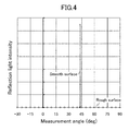
- FIG. 4 is a graph showing reflection light intensity of incident light at an incident angle of 45 degrees.
- the fine concave/convex portions 11 are formed on a smooth surface, reflection light at an output angle of about 45 degrees, i.e., regular reflection is observed.
- the surface 10 in which the fine concave/convex portions 11 are formed is a smooth surface, regular reflection of the incident light 20 can not be sufficiently suppressed.
- the fine concave/convex portions 11 are formed on a rough surface having a larger surface roughness than a wavelength of incident light, regular reflection is substantially not observed.
- the surface 10 is formed so as to be a rough surface having a larger surface roughness than a wavelength of incident light.
- the surface 10 is formed so that a surface roughness in terms of maximum height roughness Rz defined in ISO4287:1997 (JIS B0601: 2001) is larger than a wavelength of the incident light 20.
- a surface roughness in terms of maximum height roughness Rz defined in ISO4287:1997 (JIS B0601: 2001) is larger than a wavelength of the incident light 20.
- regular reflection at the surface 10 can be sufficiently suppressed. Note that the effect of suppressing the generation of regular reflection tends to be reduced when the surface roughness of the surface 10 is too large.
- a preferable range of the surface roughness Rz of the surface 10 is 100 ⁇ m or less.
- the surface roughness Rz is more preferably 50 ⁇ m and even more preferably 30 ⁇ m.
- the surface 10 on which the fine concave/convex portions 11 (SWS) are formed is formed to have a larger surface roughness than a wavelength of incident light into the surface 10, so that, as shown in FIG. 3, a sufficient antireflection effect for light at a relatively large incident angle can be also achieved while keeping low dependency of reflection coefficient on incident angle.
- FIG. 5 is a graph showing the correlation between ⁇ and reflection coefficient.
- ⁇ in FIG. 5 denotes an angle between a normal vector N 2 of a tangent plane 13 of a roughness shape of the surface 10 (in other words, a tangent plane of a shape obtained by cutting off the fine concave/convex portions 11 as high-frequency components from a shape of the surface 10 including the fine concave/convex portions 11) and a normal vector N 1 of a reference plane 12 of the surface 10 (see FIG. 7).
- ⁇ is 0 degrees (in other words, the surface 10 is a smooth surface).
- incident light has a large angle, i.e., a larger angle than 50 degrees or an even larger angle, i.e., a larger angle than 70 degrees, even with the fine concave/convex portions 11 formed, a reflection coefficient tends to be increased as an incident angle increases.
- ⁇ is increased from 0 degrees, the dependency of reflection coefficient on incident angle is reduced, so that a high antireflection effect for light at a large incident angle can be achieved.
- the percentage of an area of part in which ⁇ is 5 degrees or less per unit area is preferably less than 80%. In other words, the percentage of an area per unit area of part in which ⁇ is preferably 5 degrees or more is 20% or more. In such case, compared to the case where the fine concave/convex portions 11 are formed on a smooth surface, a reflection coefficient of light at an incident angle of 89 degrees can be reduced by about 30% or more.
- the percentage of an area per unit area of part in which ⁇ is 10 degrees or less is preferably less than 90%. In other words, the percentage of an area per unit area of the part in which ⁇ is 10 degrees or more is 10% or more. Also, in this case, compared to the case where the fine concave/convex portions 11 are formed on a smooth surface, a reflection coefficient of light at an incident angle of 89 degrees can be reduced by about 30% or more.
- the percentage of the area per unit area of the part in which ⁇ is 5 degrees or less is preferably less than 50%. In other words, the percentage of the area per unit area of the part in which ⁇ is 5 degrees or more is preferably 50% or more. Moreover, the percentage of the area per unit area of the part in which ⁇ is preferably 10 degrees or less is preferably less than 80%. In other words, the percentage of the area per unit area of the part in which ⁇ is 10 degrees or more is preferably 20% or more. In such case, compared to the case where the fine concave/convex portions 11 are formed on a smooth surface, the reflection coefficient of light at an incident angle of 89 degrees can be reduced by about 50% or more.
- the percentage of the area per unit area of the part in which ⁇ is 5 degrees or less is preferably less than 30%. In other words, the percentage of the area per unit area of the part in which ⁇ is 5 degrees or more is preferably 70% or more. Moreover, the percentage of the area per unit area of the part in which ⁇ is preferably 10 degrees or less is preferably less than 50%. In other words, the percentage of the area per unit area of the part in which ⁇ is 10 degrees or more is preferably 50% or more. In such case, compared to the case where the fine concave/convex portions 11 are formed on a smooth surface, the reflection coefficient of light at an incident angle of 89 degrees can be reduced by about 70% or more.
- FIG. 6 is a graph showing the correlation between ⁇ ave and reflection coefficient.
- ⁇ ave is preferably 5 degrees or more.
- the reflection coefficient of light at an incident angle of 89 degrees can be reduced by about 30% or more.
- ⁇ ave is 10 degrees or more.
- the reflection coefficient of light at an incident angle of 89 degrees can be reduced by about 50% or more.
- ⁇ ave is 15 degrees or more.
- the reflection coefficient of light at an incident angle of 89 degrees can be reduced by about 30% or more.
- a peak (i.e., a value of ⁇ which is most frequently included) of a ⁇ distribution is preferably larger than 0 degrees.
- the peak is more preferably 2 degrees or more, or even more preferably 5 degrees or more.
- part in which an angle ( ⁇ ) between the normal vector N 2 of the tangent plane 13 of the surface 10 and the normal vector N 1 of the reference plane 12 of the surface 10 is larger than 90 degrees does not exist.
- the surface 10 is substantially formed of a plane having a roughness shape of ⁇ ⁇ 90 degrees.
- the antireflection structure of the present invention has been described using the light transmitting diffusing plate 1 as an example.
- the antireflection structure of the present invention is not limited to a light transmitting structure but may be, for example, a light absorbing structure, i.e., a so-called black body.
- the diffusing plate 1 does not have to be a single unit body, but may be formed of a plurality of components.
- the SWS does not have to be provided throughout the surface 10, but may be formed only in necessary part.
- other part of the surface 10 may be a rough surface having the same surface roughness as the surface roughness of the part in which the SWS is provided or may be a smooth surface having a smaller surface roughness than the surface roughness of the part in which the SWS is provided.
- some other antireflection structure including a multilayer film of a film having a relatively low reflection coefficient and a film having a relatively large reflection coefficient may be formed in part in which the SWS is not formed.
- a height and a cycle (pitch) of the SWS may be adjusted as necessary.
Landscapes
- Physics & Mathematics (AREA)
- General Physics & Mathematics (AREA)
- Optics & Photonics (AREA)
- Surface Treatment Of Optical Elements (AREA)
- Optical Elements Other Than Lenses (AREA)
- Liquid Crystal (AREA)
Applications Claiming Priority (1)
| Application Number | Priority Date | Filing Date | Title |
|---|---|---|---|
| JP2006134916A JP5105771B2 (ja) | 2006-05-15 | 2006-05-15 | 反射防止構造体及びそれを備えた光学装置 |
Publications (2)
| Publication Number | Publication Date |
|---|---|
| EP1857840A2 true EP1857840A2 (fr) | 2007-11-21 |
| EP1857840A3 EP1857840A3 (fr) | 2010-03-10 |
Family
ID=38353051
Family Applications (1)
| Application Number | Title | Priority Date | Filing Date |
|---|---|---|---|
| EP07108238A Ceased EP1857840A3 (fr) | 2006-05-15 | 2007-05-15 | Structure antireflet et dispositif optique l'incorporant |
Country Status (4)
| Country | Link |
|---|---|
| US (2) | US8023190B2 (fr) |
| EP (1) | EP1857840A3 (fr) |
| JP (1) | JP5105771B2 (fr) |
| CN (1) | CN101074998A (fr) |
Cited By (1)
| Publication number | Priority date | Publication date | Assignee | Title |
|---|---|---|---|---|
| EP2544030A4 (fr) * | 2010-03-02 | 2014-09-03 | Panasonic Corp | Élément optique et procédé de fabrication d'éléments optiques |
Families Citing this family (6)
| Publication number | Priority date | Publication date | Assignee | Title |
|---|---|---|---|---|
| JP5105771B2 (ja) * | 2006-05-15 | 2012-12-26 | パナソニック株式会社 | 反射防止構造体及びそれを備えた光学装置 |
| JP4693827B2 (ja) * | 2007-09-20 | 2011-06-01 | 株式会社東芝 | 半導体装置とその製造方法 |
| JP4991001B2 (ja) * | 2009-12-28 | 2012-08-01 | シャープ株式会社 | 照明装置 |
| JP2011002853A (ja) * | 2010-09-21 | 2011-01-06 | Sony Corp | 微細加工体の製造方法、およびエッチング装置 |
| US8642965B2 (en) * | 2011-05-27 | 2014-02-04 | Raytheon Company | Stray light baffle for a seeker or other sensor system and a method for making the same |
| KR20140109103A (ko) * | 2013-03-05 | 2014-09-15 | 주식회사 엘엠에스 | 광학 시트 구조체 |
Citations (3)
| Publication number | Priority date | Publication date | Assignee | Title |
|---|---|---|---|---|
| DE19708776C1 (de) | 1997-03-04 | 1998-06-18 | Fraunhofer Ges Forschung | Entspiegelungsschicht sowie Verfahren zur Herstellung derselben |
| US20050063066A1 (en) | 2003-08-13 | 2005-03-24 | Sumitomo Chemical Company, Limited | Anti-glare optical film and process for preparing the same |
| JP2005092197A (ja) * | 2003-08-13 | 2005-04-07 | Sumitomo Chemical Co Ltd | 防眩性光学フィルム |
Family Cites Families (17)
| Publication number | Priority date | Publication date | Assignee | Title |
|---|---|---|---|---|
| JPS4911904A (fr) | 1972-05-15 | 1974-02-01 | ||
| US4944986A (en) * | 1988-09-23 | 1990-07-31 | Zuel Company | Anti-reflective glass surface |
| JP2001127852A (ja) | 1999-10-28 | 2001-05-11 | Seiko Epson Corp | カバーガラス及び光学部品 |
| US6787692B2 (en) * | 2000-10-31 | 2004-09-07 | National Institute Of Advanced Industrial Science & Technology | Solar cell substrate, thin-film solar cell, and multi-junction thin-film solar cell |
| JP2002286906A (ja) * | 2001-03-23 | 2002-10-03 | Mitsubishi Chemicals Corp | 反射防止方法及び反射防止構造並びに反射防止構造を有する反射防止構造体及びその製造方法 |
| WO2002093534A1 (fr) * | 2001-05-16 | 2002-11-21 | Bridgestone Corporation | Fenetre assurant la transmission de la lumiere et une protection contre les ondes electromagnetiques |
| JP2003114316A (ja) | 2001-10-05 | 2003-04-18 | Japan Science & Technology Corp | 光学素子 |
| JP2003279705A (ja) * | 2002-03-25 | 2003-10-02 | Sanyo Electric Co Ltd | 反射防止部材 |
| JP2004012856A (ja) * | 2002-06-07 | 2004-01-15 | Nippon Sheet Glass Co Ltd | 光学素子、光学素子の成形型および光学素子の製造方法 |
| TWI282475B (en) * | 2002-07-26 | 2007-06-11 | Chi Mei Optoelectronics Corp | Liquid crystal display device |
| JP4393042B2 (ja) * | 2002-08-05 | 2010-01-06 | 大日本印刷株式会社 | 防眩性反射防止部材、及び光学部材 |
| US7618564B2 (en) * | 2003-03-21 | 2009-11-17 | Ovd Kinegram Ag | Microstructure and method for producing microstructures |
| JP4270968B2 (ja) | 2003-07-10 | 2009-06-03 | オリンパス株式会社 | 反射防止面付光学素子を持つ光学系を備えた光学機器 |
| JP2005181361A (ja) * | 2003-12-16 | 2005-07-07 | Konica Minolta Holdings Inc | 反射防止構造を有する光学部材 |
| JP4740603B2 (ja) * | 2004-01-23 | 2011-08-03 | 富士フイルム株式会社 | 反射防止フィルムの製造方法 |
| CN100427971C (zh) * | 2004-05-27 | 2008-10-22 | 松下电器产业株式会社 | 光吸收构件 |
| JP5105771B2 (ja) * | 2006-05-15 | 2012-12-26 | パナソニック株式会社 | 反射防止構造体及びそれを備えた光学装置 |
-
2006
- 2006-05-15 JP JP2006134916A patent/JP5105771B2/ja not_active Expired - Fee Related
-
2007
- 2007-05-15 US US11/798,534 patent/US8023190B2/en not_active Expired - Fee Related
- 2007-05-15 CN CNA2007101049903A patent/CN101074998A/zh active Pending
- 2007-05-15 EP EP07108238A patent/EP1857840A3/fr not_active Ceased
-
2011
- 2011-08-15 US US13/210,107 patent/US20110299169A1/en not_active Abandoned
Patent Citations (4)
| Publication number | Priority date | Publication date | Assignee | Title |
|---|---|---|---|---|
| DE19708776C1 (de) | 1997-03-04 | 1998-06-18 | Fraunhofer Ges Forschung | Entspiegelungsschicht sowie Verfahren zur Herstellung derselben |
| JP2001517319A (ja) | 1997-03-04 | 2001-10-02 | フラウンホファー.ゲゼルシャフト.ツール.フォルデンウング.デール.アンゲヴァンドテン.フォルシュング.エー.ファウ. | 反射防止膜とその製法 |
| US20050063066A1 (en) | 2003-08-13 | 2005-03-24 | Sumitomo Chemical Company, Limited | Anti-glare optical film and process for preparing the same |
| JP2005092197A (ja) * | 2003-08-13 | 2005-04-07 | Sumitomo Chemical Co Ltd | 防眩性光学フィルム |
Non-Patent Citations (1)
| Title |
|---|
| DANIEL H. RAGUIN; G. MICHAEL MORRIS: "Analysis of antireflection-structured surfaces with continuous one-dimensional surface profiles", APPLIED OPTICS, vol. 32, no. 14, 1993, pages 2582 - 2598 |
Cited By (1)
| Publication number | Priority date | Publication date | Assignee | Title |
|---|---|---|---|---|
| EP2544030A4 (fr) * | 2010-03-02 | 2014-09-03 | Panasonic Corp | Élément optique et procédé de fabrication d'éléments optiques |
Also Published As
| Publication number | Publication date |
|---|---|
| US8023190B2 (en) | 2011-09-20 |
| US20070285784A1 (en) | 2007-12-13 |
| EP1857840A3 (fr) | 2010-03-10 |
| JP5105771B2 (ja) | 2012-12-26 |
| JP2007304467A (ja) | 2007-11-22 |
| US20110299169A1 (en) | 2011-12-08 |
| CN101074998A (zh) | 2007-11-21 |
Similar Documents
| Publication | Publication Date | Title |
|---|---|---|
| US8259394B2 (en) | Antireflection structure and optical device including the same | |
| US20110299169A1 (en) | Antireflection structure and optical device including the same | |
| JP5512269B2 (ja) | 反射防止構造体、光学ユニット及び光学装置 | |
| CN101082680B (zh) | 光吸收防反射构造体,光学单元,透镜镜筒单元和光学装置 | |
| US7226197B2 (en) | Surface light source device and light guide used therefor | |
| US5894539A (en) | Line light source having light pipe with rectangular cross-section | |
| US6570710B1 (en) | Subwavelength optical microstructure light collimating films | |
| US6356389B1 (en) | Subwavelength optical microstructure light collimating films | |
| JP5812566B2 (ja) | 発光アプリケーションのための光取り込み構造 | |
| WO2005083478A1 (fr) | Film ameliorant la luminosite utilisant un reseau concentrateur de lumiere, plaque de guidage de lumiere, systeme d'eclairage et appareil d'affichage utilisant ledit film | |
| EP2116875A2 (fr) | Conducteur de lumière et dispositif d'éclairage en disposant | |
| CN101750665A (zh) | 导光板以及使用该导光板的背光模组 | |
| JP2008532297A (ja) | 光導波体 | |
| JP2009223192A (ja) | 光学素子 | |
| JP2009258621A (ja) | レンズシート、ディスプレイ用光学シート及びそれを用いたバックライト・ユニット、ディスプレイ装置 | |
| US7559681B2 (en) | Light pipe for direct-type backlight and direct-type backlight | |
| KR101409992B1 (ko) | 휘도강화 확산필름 | |
| KR100978318B1 (ko) | 소형 백라이트 유닛용 프리즘시트 | |
| US20260107619A1 (en) | Electronic device | |
| JP2733217B2 (ja) | 内視鏡用照明光学系 | |
| JP2012150520A (ja) | 反射防止構造体及びそれを備えた光学装置 | |
| KR20100091613A (ko) | 램프 은폐성이 개선된 광학 시트 및 그를 포함한 액정표시장치 | |
| JP5201913B2 (ja) | 反射防止構造体及びそれを備えた光学装置 |
Legal Events
| Date | Code | Title | Description |
|---|---|---|---|
| PUAI | Public reference made under article 153(3) epc to a published international application that has entered the european phase |
Free format text: ORIGINAL CODE: 0009012 |
|
| AK | Designated contracting states |
Kind code of ref document: A2 Designated state(s): AT BE BG CH CY CZ DE DK EE ES FI FR GB GR HU IE IS IT LI LT LU LV MC MT NL PL PT RO SE SI SK TR |
|
| AX | Request for extension of the european patent |
Extension state: AL BA HR MK YU |
|
| RAP1 | Party data changed (applicant data changed or rights of an application transferred) |
Owner name: PANASONIC CORPORATION |
|
| PUAL | Search report despatched |
Free format text: ORIGINAL CODE: 0009013 |
|
| AK | Designated contracting states |
Kind code of ref document: A3 Designated state(s): AT BE BG CH CY CZ DE DK EE ES FI FR GB GR HU IE IS IT LI LT LU LV MC MT NL PL PT RO SE SI SK TR |
|
| AX | Request for extension of the european patent |
Extension state: AL BA HR MK RS |
|
| RIC1 | Information provided on ipc code assigned before grant |
Ipc: G02B 5/02 20060101ALI20100203BHEP Ipc: G02B 1/11 20060101AFI20070821BHEP |
|
| 17P | Request for examination filed |
Effective date: 20100910 |
|
| AKX | Designation fees paid |
Designated state(s): DE FR GB |
|
| 17Q | First examination report despatched |
Effective date: 20110617 |
|
| STAA | Information on the status of an ep patent application or granted ep patent |
Free format text: STATUS: THE APPLICATION HAS BEEN REFUSED |
|
| 18R | Application refused |
Effective date: 20131114 |