EP1858065A2 - Procédé de fabrication d'un élément semi-conducteur doté d'une électrode porte métallique agencée dans une double structure à tranchée - Google Patents
Procédé de fabrication d'un élément semi-conducteur doté d'une électrode porte métallique agencée dans une double structure à tranchée Download PDFInfo
- Publication number
- EP1858065A2 EP1858065A2 EP07009106A EP07009106A EP1858065A2 EP 1858065 A2 EP1858065 A2 EP 1858065A2 EP 07009106 A EP07009106 A EP 07009106A EP 07009106 A EP07009106 A EP 07009106A EP 1858065 A2 EP1858065 A2 EP 1858065A2
- Authority
- EP
- European Patent Office
- Prior art keywords
- layer
- opening
- auxiliary layer
- gate
- depositing
- Prior art date
- Legal status (The legal status is an assumption and is not a legal conclusion. Google has not performed a legal analysis and makes no representation as to the accuracy of the status listed.)
- Granted
Links
Images
Classifications
-
- H—ELECTRICITY
- H10—SEMICONDUCTOR DEVICES; ELECTRIC SOLID-STATE DEVICES NOT OTHERWISE PROVIDED FOR
- H10D—INORGANIC ELECTRIC SEMICONDUCTOR DEVICES
- H10D64/00—Electrodes of devices having potential barriers
- H10D64/20—Electrodes characterised by their shapes, relative sizes or dispositions
- H10D64/27—Electrodes not carrying the current to be rectified, amplified, oscillated or switched, e.g. gates
- H10D64/311—Gate electrodes for field-effect devices
- H10D64/411—Gate electrodes for field-effect devices for FETs
-
- H—ELECTRICITY
- H10—SEMICONDUCTOR DEVICES; ELECTRIC SOLID-STATE DEVICES NOT OTHERWISE PROVIDED FOR
- H10D—INORGANIC ELECTRIC SEMICONDUCTOR DEVICES
- H10D30/00—Field-effect transistors [FET]
- H10D30/01—Manufacture or treatment
- H10D30/015—Manufacture or treatment of FETs having heterojunction interface channels or heterojunction gate electrodes, e.g. HEMT
-
- H—ELECTRICITY
- H10—SEMICONDUCTOR DEVICES; ELECTRIC SOLID-STATE DEVICES NOT OTHERWISE PROVIDED FOR
- H10D—INORGANIC ELECTRIC SEMICONDUCTOR DEVICES
- H10D30/00—Field-effect transistors [FET]
- H10D30/40—FETs having zero-dimensional [0D], one-dimensional [1D] or two-dimensional [2D] charge carrier gas channels
- H10D30/47—FETs having zero-dimensional [0D], one-dimensional [1D] or two-dimensional [2D] charge carrier gas channels having two-dimensional [2D] charge carrier gas channels, e.g. nanoribbon FETs or high electron mobility transistors [HEMT]
- H10D30/471—High electron mobility transistors [HEMT] or high hole mobility transistors [HHMT]
- H10D30/475—High electron mobility transistors [HEMT] or high hole mobility transistors [HHMT] having wider bandgap layer formed on top of lower bandgap active layer, e.g. undoped barrier HEMTs such as i-AlGaN/GaN HEMTs
-
- H—ELECTRICITY
- H10—SEMICONDUCTOR DEVICES; ELECTRIC SOLID-STATE DEVICES NOT OTHERWISE PROVIDED FOR
- H10D—INORGANIC ELECTRIC SEMICONDUCTOR DEVICES
- H10D64/00—Electrodes of devices having potential barriers
- H10D64/01—Manufacture or treatment
- H10D64/012—Manufacture or treatment of electrodes comprising a Schottky barrier to a semiconductor
- H10D64/0124—Manufacture or treatment of electrodes comprising a Schottky barrier to a semiconductor to Group III-V semiconductors
- H10D64/0125—Manufacture or treatment of electrodes comprising a Schottky barrier to a semiconductor to Group III-V semiconductors characterised by the sectional shape, e.g. T or inverted T
Definitions
- the invention relates to a method for producing a semiconductor component, in particular a pHEMT field effect transistor, having a metallic gate electrode arranged in a double trench structure.
- Double recess Semiconductor components having a gate electrode arranged in a double trench structure, also referred to as double recess, are known in various designs.
- the US 2004/0082158 A1 describes a method in which a plurality of photoresist layers are deposited on the semiconductor layer sequence, in which structures are prepared for the gate head for a later production of a T-shaped gate electrode in the lift-off method.
- a lacquer layer deposited on the highly doped contact layer of the semiconductor layer sequence an opening defining the structure of the gate foot is produced.
- the lacquer layers remain in the following process steps up to Evaporation of the gate metal obtained.
- Under the lowest resist layer a trench structure is produced up to a barrier layer by undercutting in the contact layer, and gate metal is deposited through the opening of the lowermost resist layer on the barrier layer and simultaneously into the structures of the top resist layers to form the gate. By dissolving the lacquer layers, the gate electrode is exposed. Thereafter, ohmic contacts are still generated on the highly doped contact layer.
- the invention has for its object to provide an advantageous method for producing a semiconductor device with a metallic gate electrode and a double trench structure.
- the generation of the double trench structure is advantageously carried out by the method according to the invention in self-aligning positioning of the wide and narrow trenches in several steps, wherein structures generated in intermediate steps can advantageously serve as masking for subsequent etching steps. Also for the gate foot results in a self-centering position within the narrow trench.
- both the position of the wide trench by undercutting the first auxiliary layer and the position of the narrow trench by transferring the structure of the first opening in a further opening of another auxiliary layer and its undercut are determined and thus a reliable Self-aligning mutual lateral alignment of the wide and narrow trench can be achieved.
- a further auxiliary layer is deposited through the first opening into the second trench and there in particular onto the shielding layer, and the further opening produced in this further auxiliary layer serves as a hard mask for the etching of the narrow trench.
- the broad trench is preferably filled with a solidifiable liquid filling material, preferably a polymerizable material, and the material is in particular solidified to a polymer.
- the transfer of the structure of the first opening then advantageously takes place into a second opening in the polymer and the further auxiliary layer located between the polymer and the shielding layer.
- the first auxiliary layer is removed above the polymer or, preferably, as a whole, and gate metal for the gate head is deposited on the polymer.
- etchants known in many ways in composition and application, which can be selected and used in particular material-selectively.
- the inventive method includes a highly scalable and self-aligned integration to define the gate area with gate base and gate head.
- the gate foot can dimensions of z. B. 70-600 nm, while the gate head can typically be wider on both sides by 50-300 nm.
- the gate base is centered in a narrow trench in the shielding layer, which in turn is centered to the wide trench in the heavily doped contact layer.
- the wide trench is typically on both sides 200 mm - 1000 mm wider than the narrow trench.
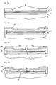
- the layers 1-5 in Fig. 1a define the vertical profile of a field effect transistor, in particular a pHEMT high frequency power field effect transistor, which may vary in thickness and element structure depending on the application.
- the layer thickness ratios are not to scale.
- 1 represents the buffer
- 2 forms the channel layer for the two-dimensional electron gas
- 3 is a barrier layer preferably with overhead stop layer
- 4 is a low-doped shielding layer, which also preferably terminates upwards with a stop layer
- the layer 5 forms as the uppermost semiconductor layer a highly doped contact layer for low-resistance component contacting.
- the layers 4 and 5 are preferably made of GaAs and the stop layers advantageously of AIAs or InGaP.
- a dielectric interlayer 8 preferably an SiO 2 layer and a dielectric auxiliary layer 9, preferably a silicon nitride (SiN) layer, preferably by PECVD.
- the lateral isolation of the transistors takes place by means of a photoresist masked implantation to form isolated field regions 7 (FIG. 1b).
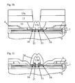
- a photoresist layer is applied and a lithography mask with a structure for the gate foot relative to Adjusted to the ohmic contacts.
- the opening 11 is formed in the photoresist 10 a, which z. B. is transferred by dry chemical plasma etching in the underlying double layer of first auxiliary layer 9 and intermediate layer 8, so that in these layers openings 9a and 8a arise (Fig. 1c).
- the photoresist 10a is then removed again.
- the opening 8a in the intermediate layer 8 is widened to a larger opening 8b whose lateral width is easily adjustable via the parameters of the etching process, in particular its duration.
- the opening 8b in the intermediate layer serves in a subsequent etching step as a hard mask for etching the wide trench 50 in the contact layer 5, wherein the ⁇ tzstop für between the shielding layer and contact layer vertically delimits the etching, and the structure of FIG. 1d arises.
- auxiliary layer preferably SiN deposited, wherein the deposition as a uniform layer 90a on the first auxiliary layer and through the opening 9a in the first auxiliary layer as a hard mask layer 90b in the cavity formed by the opening 8b and the wide trench 50 below the first Auxiliary layer, and there in particular on the shielding layer 4 and at the edges of the opening in the first auxiliary layer now designated 9b, takes place.
- the further auxiliary layer 90b is deposited on the shielding layer 4 with respect to the opening 9a of greater width or on the entire inner surface of the cavity, wherein the layer thickness of further auxiliary layer 90b on the shielding layer is less than the layer thickness of the further auxiliary layer 90a on the first auxiliary layer.
- a polymer, in particular BCB, is then applied, which in addition to a layer on 100a on the first auxiliary layer 9 also fills the opening 9b with a portion 100b and the cavity formed under the first auxiliary layer through the opening 8b and the wide trench 50 (FIG. 1e).
- the polymer layer is extensively and partly also the further auxiliary layer 100a removed by a subsequent full-area plasma etching back (FIG. 1f), after which the structure of the opening 9b in the first auxiliary layer is transferred as opening 10 into the polymer layer 100b and as opening 900b into the further auxiliary layer 90b ,
- the first auxiliary layer is advantageously completely removed and the polymer filling the cavity exposed as lateral boundaries 100c of the opening 10, so that the structure outlined in Fig. 1g is formed.
- the properties of the various materials of the intermediate layer 8, the first auxiliary layer 9, the second auxiliary layer 90a, 90b and the polymer 100a, 100b for selective etching can be utilized by suitable settings of the etching parameters.
- the opening 10 delimited laterally by the polymer 100c and the opening 900b as a hard mask in the further auxiliary layer 90b form the lateral boundary for a subsequent etching of the narrow trench by etching the shielding layer 4 in the opening 900b and laterally thereof under the further auxiliary layer 90b.
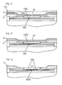
- a mask structure for the gate head is produced for the production of the gate head in lift-off technology in a photolithographic process.
- two photoresist layers 11 and 12 are deposited on the sketched in Fig. 1g arrangement, wherein preferably a lower lacquer layer of PGMI and an upper lacquer layer 12 of a thin positive paint exists.
- a width of the gate head defining opening in the upper lacquer layer 12 and a laterally larger opening in the lower lacquer layer 11 is formed.
- a narrow trench 15 in the shielding layer 4 up to the barrier layer 3 is produced with the openings 10 in the polymer 100c and 900b in the further auxiliary layer 90b, which widens by a small amount by defined lateral undercutting of the further auxiliary layer 90b is as the opening 90b.
- the barrier layer is covered by the portions 16 of the shielding layer.
- gate metal is vapor deposited, which forms the gate base in the narrow trench and the openings 900b and 10 and the gate head 13b of a T-shaped gate electrode over the polymer 100c.
- the upper surface of the polymer layers 100c can thereby advantageously serve for the defined adjustment of the lower edge of the overhanging lateral region of the gate head.
- the upper surface of the polymer layers 100c substantially coincides with the upper surface of the intermediate layer 8 between the ohmic contacts 6 and therefore can already be predetermined during the deposition of the intermediate layer 8.
- the polymer 100c, the additional auxiliary layer 90b and the intermediate layer 8 are removed, for which advantageously a CF 4 -based plasma can be used.
- a passivation layer 20, preferably SiN, is formed over the whole area, in particular also into the trenches 50, 15 below the overhanging lateral gate head areas, wherein the passivation layer includes cavities 21 under the overhanging gate head regions ( Figure 1 i). Through the cavities 21 feedback capacitances can be reduced in a particularly advantageous manner.
Landscapes
- Junction Field-Effect Transistors (AREA)
- Electrodes Of Semiconductors (AREA)
Applications Claiming Priority (1)
| Application Number | Priority Date | Filing Date | Title |
|---|---|---|---|
| DE102006022508A DE102006022508A1 (de) | 2006-05-15 | 2006-05-15 | Verfahren zur Herstellung eines Halbleiterbauelements mit einer in einer Doppelgrabenstruktur angeordneten metallischen Gateelektrode |
Publications (3)
| Publication Number | Publication Date |
|---|---|
| EP1858065A2 true EP1858065A2 (fr) | 2007-11-21 |
| EP1858065A3 EP1858065A3 (fr) | 2008-05-28 |
| EP1858065B1 EP1858065B1 (fr) | 2011-02-16 |
Family
ID=38370366
Family Applications (1)
| Application Number | Title | Priority Date | Filing Date |
|---|---|---|---|
| EP07009106A Not-in-force EP1858065B1 (fr) | 2006-05-15 | 2007-05-05 | Procédé de fabrication d'un élément semi-conducteur doté d'une électrode porte métallique agencée dans une double structure à tranchée |
Country Status (4)
| Country | Link |
|---|---|
| US (1) | US7618851B2 (fr) |
| EP (1) | EP1858065B1 (fr) |
| AT (1) | ATE498905T1 (fr) |
| DE (2) | DE102006022508A1 (fr) |
Families Citing this family (4)
| Publication number | Priority date | Publication date | Assignee | Title |
|---|---|---|---|---|
| JP5217301B2 (ja) | 2007-08-28 | 2013-06-19 | 富士通株式会社 | 化合物半導体装置とその製造方法 |
| US9048184B2 (en) * | 2013-03-15 | 2015-06-02 | Northrop Grumman Systems Corporation | Method of forming a gate contact |
| US9583589B1 (en) | 2015-10-14 | 2017-02-28 | Northrop Grumman Systems Corporation | Self-aligned double gate recess for semiconductor field effect transistors |
| US11881506B2 (en) * | 2021-07-27 | 2024-01-23 | Globalfoundries U.S. Inc. | Gate structures with air gap isolation features |
Citations (1)
| Publication number | Priority date | Publication date | Assignee | Title |
|---|---|---|---|---|
| US6180968B1 (en) | 1996-05-31 | 2001-01-30 | Nec Corporation | Compound semiconductor device and method of manufacturing the same |
Family Cites Families (11)
| Publication number | Priority date | Publication date | Assignee | Title |
|---|---|---|---|---|
| EP0592064B1 (fr) * | 1992-08-19 | 1998-09-23 | Mitsubishi Denki Kabushiki Kaisha | Méthode de fabrication d'un transistor à effet de champ |
| JPH06275655A (ja) * | 1993-03-24 | 1994-09-30 | Mitsubishi Electric Corp | 半導体装置及びその製造方法 |
| JP2643859B2 (ja) | 1994-09-29 | 1997-08-20 | 日本電気株式会社 | 化合物半導体電界効果トランジスタ |
| US5556797A (en) | 1995-05-30 | 1996-09-17 | Hughes Aircraft Company | Method of fabricating a self-aligned double recess gate profile |
| JPH0936133A (ja) | 1995-07-14 | 1997-02-07 | Mitsubishi Electric Corp | 半導体装置およびその製造方法 |
| JP2904167B2 (ja) * | 1996-12-18 | 1999-06-14 | 日本電気株式会社 | 半導体装置の製造方法 |
| DE10101825B4 (de) * | 2001-01-17 | 2006-12-14 | United Monolithic Semiconductors Gmbh | Verfahren zur Herstellung eines Halbleiter-Bauelements mit einer T-förmigen Kontaktelektrode |
| DE10117741B4 (de) * | 2001-04-09 | 2008-05-21 | United Monolithic Semiconductors Gmbh | Verfahren zur Herstellung eines Halbleiter-Bauelements mit T-förmigen Kontaktelektrode |
| DE10220999A1 (de) * | 2003-02-06 | 2003-11-20 | United Monolithic Semiconduct | Verfahren zur Herstellung eines Halbleiterbauelements und danach hergestelltes Halbleiterelement |
| US6838325B2 (en) * | 2002-10-24 | 2005-01-04 | Raytheon Company | Method of forming a self-aligned, selectively etched, double recess high electron mobility transistor |
| JP4284254B2 (ja) * | 2004-09-07 | 2009-06-24 | 富士通株式会社 | 電界効果型半導体装置 |
-
2006
- 2006-05-15 DE DE102006022508A patent/DE102006022508A1/de not_active Withdrawn
-
2007
- 2007-05-05 DE DE502007006491T patent/DE502007006491D1/de active Active
- 2007-05-05 EP EP07009106A patent/EP1858065B1/fr not_active Not-in-force
- 2007-05-05 AT AT07009106T patent/ATE498905T1/de active
- 2007-05-07 US US11/800,769 patent/US7618851B2/en not_active Expired - Fee Related
Patent Citations (1)
| Publication number | Priority date | Publication date | Assignee | Title |
|---|---|---|---|---|
| US6180968B1 (en) | 1996-05-31 | 2001-01-30 | Nec Corporation | Compound semiconductor device and method of manufacturing the same |
Also Published As
| Publication number | Publication date |
|---|---|
| ATE498905T1 (de) | 2011-03-15 |
| US7618851B2 (en) | 2009-11-17 |
| DE102006022508A1 (de) | 2007-11-22 |
| US20070264763A1 (en) | 2007-11-15 |
| EP1858065A3 (fr) | 2008-05-28 |
| EP1858065B1 (fr) | 2011-02-16 |
| DE502007006491D1 (de) | 2011-03-31 |
Similar Documents
| Publication | Publication Date | Title |
|---|---|---|
| EP1508164B1 (fr) | Procede de production d'un composant semi-conducteur et composant semi-conducteur ainsi produit | |
| EP0352736B1 (fr) | Procédé pour la réalisation d'une structure de laque sur un matériau semiconducteur ayant une ouverture se rétrécissant vers le matériau semiconducteur | |
| DE69126463T2 (de) | Verfahren zur Herstellung eines leitenden Elements | |
| DE102008059650B4 (de) | Verfahren zur Herstellung einer Mikrostruktur mit einer Metallisierungsstruktur mit selbstjustierten Luftspalten zwischen dichtliegenden Metallleitungen | |
| DE4138842C2 (de) | Gateelektrode und Verfahren zu deren Herstellung | |
| EP1858064B1 (fr) | Procédé de fabrication d'un élément semi-conducteur doté d'une électrode porte métallique agencée dans une double structure à tranchée | |
| DE10219398B4 (de) | Herstellungsverfahren für eine Grabenanordnung mit Gräben unterschiedlicher Tiefe in einem Halbleitersubstrat | |
| DE2723944A1 (de) | Anordnung aus einer strukturierten schicht und einem muster festgelegter dicke und verfahren zu ihrer herstellung | |
| EP1354342B1 (fr) | Procede pour fabriquer un composant semi-conducteur comportant une electrode de contact en forme de t | |
| DE4413152A1 (de) | Verfahren zur Strukturerzeugung in einem Halbleiterbauelement | |
| EP1858065B1 (fr) | Procédé de fabrication d'un élément semi-conducteur doté d'une électrode porte métallique agencée dans une double structure à tranchée | |
| DE60222046T2 (de) | Verfahren zur Herstellung HBT-Anordnungen | |
| DE60206012T2 (de) | Verfahren zur Herstellung einer T-förmigen Elektrode | |
| DE68922474T2 (de) | Verfahren zum Herstellen einer integrierten Schaltung einschliesslich Schritte zum Herstellen einer Verbindung zwischen zwei Schichten. | |
| DE102007030020B4 (de) | Verfahren zum Ausbilden einer Halbleiterstruktur mit einem Ausbilden von mindestens einer Seitenwandabstandshalterstruktur | |
| DE3888511T2 (de) | Verfahren zum Herstellen von elektrischen Kontakten in integrierten Schaltungen. | |
| DE69509698T2 (de) | Verfahren zur Herstellung eines Feldeffekttransistors mit isoliertem Gate und kurzem Kanal, und entsprechender Transistor | |
| WO2002078058A2 (fr) | Procede pour la production d'un transistor mosfet a longueur de canal tres faible | |
| DE102016105255A1 (de) | Erzeugung von Isolationsgräben unterschiedlicher Tiefe in einem Halbleitersubstrat | |
| EP1380047B1 (fr) | Procede de production d'un composant semi-conducteur presentant une electrode de contact en forme de t | |
| DE10225525A1 (de) | Verfahren zur Herstellung eines Hetero-Bipolar-Transistors und Hetero-Bipolar-Transistor | |
| DE10052131C2 (de) | Verfahren zur Herstellung von Feldeffekttransistoren mit einer vollständig selbstjustierenden Technologie | |
| EP0358042B1 (fr) | Procédé autoaligné pour la fabrication d'une électrode de porte | |
| DE19530050C2 (de) | Selbstjustierendes Verfahren zur Herstellung von Feldeffekttransistoren | |
| DE102004031111B4 (de) | Verfahren zum Herstellen sublithografischer Gate-Strukturen eines Feldeffekttransistoren |
Legal Events
| Date | Code | Title | Description |
|---|---|---|---|
| PUAI | Public reference made under article 153(3) epc to a published international application that has entered the european phase |
Free format text: ORIGINAL CODE: 0009012 |
|
| AK | Designated contracting states |
Kind code of ref document: A2 Designated state(s): AT BE BG CH CY CZ DE DK EE ES FI FR GB GR HU IE IS IT LI LT LU LV MC MT NL PL PT RO SE SI SK TR |
|
| AX | Request for extension of the european patent |
Extension state: AL BA HR MK YU |
|
| PUAL | Search report despatched |
Free format text: ORIGINAL CODE: 0009013 |
|
| AK | Designated contracting states |
Kind code of ref document: A3 Designated state(s): AT BE BG CH CY CZ DE DK EE ES FI FR GB GR HU IE IS IT LI LT LU LV MC MT NL PL PT RO SE SI SK TR |
|
| AX | Request for extension of the european patent |
Extension state: AL BA HR MK RS |
|
| 17P | Request for examination filed |
Effective date: 20081128 |
|
| AKX | Designation fees paid |
Designated state(s): AT BE BG CH CY CZ DE DK EE ES FI FR GB GR HU IE IS IT LI LT LU LV MC MT NL PL PT RO SE SI SK TR |
|
| 17Q | First examination report despatched |
Effective date: 20090211 |
|
| GRAP | Despatch of communication of intention to grant a patent |
Free format text: ORIGINAL CODE: EPIDOSNIGR1 |
|
| GRAS | Grant fee paid |
Free format text: ORIGINAL CODE: EPIDOSNIGR3 |
|
| GRAA | (expected) grant |
Free format text: ORIGINAL CODE: 0009210 |
|
| AK | Designated contracting states |
Kind code of ref document: B1 Designated state(s): AT BE BG CH CY CZ DE DK EE ES FI FR GB GR HU IE IS IT LI LT LU LV MC MT NL PL PT RO SE SI SK TR |
|
| REG | Reference to a national code |
Ref country code: GB Ref legal event code: FG4D Free format text: NOT ENGLISH |
|
| REG | Reference to a national code |
Ref country code: CH Ref legal event code: EP |
|
| REG | Reference to a national code |
Ref country code: IE Ref legal event code: FG4D Free format text: LANGUAGE OF EP DOCUMENT: GERMAN |
|
| REF | Corresponds to: |
Ref document number: 502007006491 Country of ref document: DE Date of ref document: 20110331 Kind code of ref document: P |
|
| REG | Reference to a national code |
Ref country code: DE Ref legal event code: R096 Ref document number: 502007006491 Country of ref document: DE Effective date: 20110331 |
|
| REG | Reference to a national code |
Ref country code: NL Ref legal event code: VDEP Effective date: 20110216 |
|
| LTIE | Lt: invalidation of european patent or patent extension |
Effective date: 20110216 |
|
| PG25 | Lapsed in a contracting state [announced via postgrant information from national office to epo] |
Ref country code: PT Free format text: LAPSE BECAUSE OF FAILURE TO SUBMIT A TRANSLATION OF THE DESCRIPTION OR TO PAY THE FEE WITHIN THE PRESCRIBED TIME-LIMIT Effective date: 20110616 Ref country code: LT Free format text: LAPSE BECAUSE OF FAILURE TO SUBMIT A TRANSLATION OF THE DESCRIPTION OR TO PAY THE FEE WITHIN THE PRESCRIBED TIME-LIMIT Effective date: 20110216 Ref country code: GR Free format text: LAPSE BECAUSE OF FAILURE TO SUBMIT A TRANSLATION OF THE DESCRIPTION OR TO PAY THE FEE WITHIN THE PRESCRIBED TIME-LIMIT Effective date: 20110517 Ref country code: ES Free format text: LAPSE BECAUSE OF FAILURE TO SUBMIT A TRANSLATION OF THE DESCRIPTION OR TO PAY THE FEE WITHIN THE PRESCRIBED TIME-LIMIT Effective date: 20110527 Ref country code: SE Free format text: LAPSE BECAUSE OF FAILURE TO SUBMIT A TRANSLATION OF THE DESCRIPTION OR TO PAY THE FEE WITHIN THE PRESCRIBED TIME-LIMIT Effective date: 20110216 Ref country code: LV Free format text: LAPSE BECAUSE OF FAILURE TO SUBMIT A TRANSLATION OF THE DESCRIPTION OR TO PAY THE FEE WITHIN THE PRESCRIBED TIME-LIMIT Effective date: 20110216 |
|
| PG25 | Lapsed in a contracting state [announced via postgrant information from national office to epo] |
Ref country code: BG Free format text: LAPSE BECAUSE OF FAILURE TO SUBMIT A TRANSLATION OF THE DESCRIPTION OR TO PAY THE FEE WITHIN THE PRESCRIBED TIME-LIMIT Effective date: 20110516 Ref country code: NL Free format text: LAPSE BECAUSE OF FAILURE TO SUBMIT A TRANSLATION OF THE DESCRIPTION OR TO PAY THE FEE WITHIN THE PRESCRIBED TIME-LIMIT Effective date: 20110216 Ref country code: FI Free format text: LAPSE BECAUSE OF FAILURE TO SUBMIT A TRANSLATION OF THE DESCRIPTION OR TO PAY THE FEE WITHIN THE PRESCRIBED TIME-LIMIT Effective date: 20110216 Ref country code: PL Free format text: LAPSE BECAUSE OF FAILURE TO SUBMIT A TRANSLATION OF THE DESCRIPTION OR TO PAY THE FEE WITHIN THE PRESCRIBED TIME-LIMIT Effective date: 20110216 Ref country code: CY Free format text: LAPSE BECAUSE OF FAILURE TO SUBMIT A TRANSLATION OF THE DESCRIPTION OR TO PAY THE FEE WITHIN THE PRESCRIBED TIME-LIMIT Effective date: 20110216 Ref country code: SI Free format text: LAPSE BECAUSE OF FAILURE TO SUBMIT A TRANSLATION OF THE DESCRIPTION OR TO PAY THE FEE WITHIN THE PRESCRIBED TIME-LIMIT Effective date: 20110216 |
|
| REG | Reference to a national code |
Ref country code: IE Ref legal event code: FD4D |
|
| PG25 | Lapsed in a contracting state [announced via postgrant information from national office to epo] |
Ref country code: DK Free format text: LAPSE BECAUSE OF FAILURE TO SUBMIT A TRANSLATION OF THE DESCRIPTION OR TO PAY THE FEE WITHIN THE PRESCRIBED TIME-LIMIT Effective date: 20110216 Ref country code: IE Free format text: LAPSE BECAUSE OF FAILURE TO SUBMIT A TRANSLATION OF THE DESCRIPTION OR TO PAY THE FEE WITHIN THE PRESCRIBED TIME-LIMIT Effective date: 20110216 Ref country code: EE Free format text: LAPSE BECAUSE OF FAILURE TO SUBMIT A TRANSLATION OF THE DESCRIPTION OR TO PAY THE FEE WITHIN THE PRESCRIBED TIME-LIMIT Effective date: 20110216 |
|
| BERE | Be: lapsed |
Owner name: UNITED MONOLITHIC SEMICONDUCTORS G.M.B.H. Effective date: 20110531 |
|
| PG25 | Lapsed in a contracting state [announced via postgrant information from national office to epo] |
Ref country code: CZ Free format text: LAPSE BECAUSE OF FAILURE TO SUBMIT A TRANSLATION OF THE DESCRIPTION OR TO PAY THE FEE WITHIN THE PRESCRIBED TIME-LIMIT Effective date: 20110216 Ref country code: SK Free format text: LAPSE BECAUSE OF FAILURE TO SUBMIT A TRANSLATION OF THE DESCRIPTION OR TO PAY THE FEE WITHIN THE PRESCRIBED TIME-LIMIT Effective date: 20110216 Ref country code: RO Free format text: LAPSE BECAUSE OF FAILURE TO SUBMIT A TRANSLATION OF THE DESCRIPTION OR TO PAY THE FEE WITHIN THE PRESCRIBED TIME-LIMIT Effective date: 20110216 |
|
| PLBE | No opposition filed within time limit |
Free format text: ORIGINAL CODE: 0009261 |
|
| STAA | Information on the status of an ep patent application or granted ep patent |
Free format text: STATUS: NO OPPOSITION FILED WITHIN TIME LIMIT |
|
| PG25 | Lapsed in a contracting state [announced via postgrant information from national office to epo] |
Ref country code: MT Free format text: LAPSE BECAUSE OF FAILURE TO SUBMIT A TRANSLATION OF THE DESCRIPTION OR TO PAY THE FEE WITHIN THE PRESCRIBED TIME-LIMIT Effective date: 20110216 Ref country code: MC Free format text: LAPSE BECAUSE OF NON-PAYMENT OF DUE FEES Effective date: 20110531 |
|
| REG | Reference to a national code |
Ref country code: CH Ref legal event code: PL |
|
| 26N | No opposition filed |
Effective date: 20111117 |
|
| PG25 | Lapsed in a contracting state [announced via postgrant information from national office to epo] |
Ref country code: LI Free format text: LAPSE BECAUSE OF NON-PAYMENT OF DUE FEES Effective date: 20110531 Ref country code: CH Free format text: LAPSE BECAUSE OF NON-PAYMENT OF DUE FEES Effective date: 20110531 |
|
| REG | Reference to a national code |
Ref country code: DE Ref legal event code: R097 Ref document number: 502007006491 Country of ref document: DE Effective date: 20111117 |
|
| PG25 | Lapsed in a contracting state [announced via postgrant information from national office to epo] |
Ref country code: BE Free format text: LAPSE BECAUSE OF NON-PAYMENT OF DUE FEES Effective date: 20110531 |
|
| PG25 | Lapsed in a contracting state [announced via postgrant information from national office to epo] |
Ref country code: IT Free format text: LAPSE BECAUSE OF FAILURE TO SUBMIT A TRANSLATION OF THE DESCRIPTION OR TO PAY THE FEE WITHIN THE PRESCRIBED TIME-LIMIT Effective date: 20110216 |
|
| PG25 | Lapsed in a contracting state [announced via postgrant information from national office to epo] |
Ref country code: LU Free format text: LAPSE BECAUSE OF NON-PAYMENT OF DUE FEES Effective date: 20110505 |
|
| REG | Reference to a national code |
Ref country code: AT Ref legal event code: MM01 Ref document number: 498905 Country of ref document: AT Kind code of ref document: T Effective date: 20120505 |
|
| PG25 | Lapsed in a contracting state [announced via postgrant information from national office to epo] |
Ref country code: IS Free format text: LAPSE BECAUSE OF FAILURE TO SUBMIT A TRANSLATION OF THE DESCRIPTION OR TO PAY THE FEE WITHIN THE PRESCRIBED TIME-LIMIT Effective date: 20110216 Ref country code: AT Free format text: LAPSE BECAUSE OF NON-PAYMENT OF DUE FEES Effective date: 20120505 |
|
| PG25 | Lapsed in a contracting state [announced via postgrant information from national office to epo] |
Ref country code: TR Free format text: LAPSE BECAUSE OF FAILURE TO SUBMIT A TRANSLATION OF THE DESCRIPTION OR TO PAY THE FEE WITHIN THE PRESCRIBED TIME-LIMIT Effective date: 20110216 |
|
| PG25 | Lapsed in a contracting state [announced via postgrant information from national office to epo] |
Ref country code: HU Free format text: LAPSE BECAUSE OF FAILURE TO SUBMIT A TRANSLATION OF THE DESCRIPTION OR TO PAY THE FEE WITHIN THE PRESCRIBED TIME-LIMIT Effective date: 20110216 |
|
| REG | Reference to a national code |
Ref country code: DE Ref legal event code: R082 Ref document number: 502007006491 Country of ref document: DE Representative=s name: BAUR & WEBER PATENTANWAELTE PARTG MBB, DE Ref country code: DE Ref legal event code: R082 Ref document number: 502007006491 Country of ref document: DE Representative=s name: BAUR & WEBER PATENTANWAELTE, DE |
|
| REG | Reference to a national code |
Ref country code: FR Ref legal event code: PLFP Year of fee payment: 10 |
|
| REG | Reference to a national code |
Ref country code: FR Ref legal event code: PLFP Year of fee payment: 11 |
|
| REG | Reference to a national code |
Ref country code: FR Ref legal event code: PLFP Year of fee payment: 12 |
|
| PGFP | Annual fee paid to national office [announced via postgrant information from national office to epo] |
Ref country code: DE Payment date: 20190531 Year of fee payment: 13 |
|
| PGFP | Annual fee paid to national office [announced via postgrant information from national office to epo] |
Ref country code: FR Payment date: 20190521 Year of fee payment: 13 |
|
| PGFP | Annual fee paid to national office [announced via postgrant information from national office to epo] |
Ref country code: GB Payment date: 20190523 Year of fee payment: 13 |
|
| REG | Reference to a national code |
Ref country code: DE Ref legal event code: R119 Ref document number: 502007006491 Country of ref document: DE |
|
| GBPC | Gb: european patent ceased through non-payment of renewal fee |
Effective date: 20200505 |
|
| PG25 | Lapsed in a contracting state [announced via postgrant information from national office to epo] |
Ref country code: GB Free format text: LAPSE BECAUSE OF NON-PAYMENT OF DUE FEES Effective date: 20200505 Ref country code: FR Free format text: LAPSE BECAUSE OF NON-PAYMENT OF DUE FEES Effective date: 20200531 |
|
| PG25 | Lapsed in a contracting state [announced via postgrant information from national office to epo] |
Ref country code: DE Free format text: LAPSE BECAUSE OF NON-PAYMENT OF DUE FEES Effective date: 20201201 |