EP1860676A1 - Dispositif d'affichage à plasma et procédé de fabrication de phosphore vert pour ledit dispositif d'affichage - Google Patents
Dispositif d'affichage à plasma et procédé de fabrication de phosphore vert pour ledit dispositif d'affichage Download PDFInfo
- Publication number
- EP1860676A1 EP1860676A1 EP07714543A EP07714543A EP1860676A1 EP 1860676 A1 EP1860676 A1 EP 1860676A1 EP 07714543 A EP07714543 A EP 07714543A EP 07714543 A EP07714543 A EP 07714543A EP 1860676 A1 EP1860676 A1 EP 1860676A1
- Authority
- EP
- European Patent Office
- Prior art keywords
- sio
- coated
- ratio
- discharge
- display device
- Prior art date
- Legal status (The legal status is an assumption and is not a legal conclusion. Google has not performed a legal analysis and makes no representation as to the accuracy of the status listed.)
- Withdrawn
Links
Images



Classifications
-
- C—CHEMISTRY; METALLURGY
- C09—DYES; PAINTS; POLISHES; NATURAL RESINS; ADHESIVES; COMPOSITIONS NOT OTHERWISE PROVIDED FOR; APPLICATIONS OF MATERIALS NOT OTHERWISE PROVIDED FOR
- C09K—MATERIALS FOR MISCELLANEOUS APPLICATIONS, NOT PROVIDED FOR ELSEWHERE
- C09K11/00—Luminescent materials, e.g. electroluminescent or chemiluminescent
- C09K11/08—Luminescent materials, e.g. electroluminescent or chemiluminescent containing inorganic luminescent materials
- C09K11/59—Luminescent materials, e.g. electroluminescent or chemiluminescent containing inorganic luminescent materials containing silicon
-
- H—ELECTRICITY
- H01—ELECTRIC ELEMENTS
- H01J—ELECTRIC DISCHARGE TUBES OR DISCHARGE LAMPS
- H01J11/00—Gas-filled discharge tubes with alternating current induction of the discharge, e.g. alternating current plasma display panels [AC-PDP]; Gas-filled discharge tubes without any main electrode inside the vessel; Gas-filled discharge tubes with at least one main electrode outside the vessel
- H01J11/20—Constructional details
- H01J11/34—Vessels, containers or parts thereof, e.g. substrates
- H01J11/42—Fluorescent layers
-
- C—CHEMISTRY; METALLURGY
- C09—DYES; PAINTS; POLISHES; NATURAL RESINS; ADHESIVES; COMPOSITIONS NOT OTHERWISE PROVIDED FOR; APPLICATIONS OF MATERIALS NOT OTHERWISE PROVIDED FOR
- C09K—MATERIALS FOR MISCELLANEOUS APPLICATIONS, NOT PROVIDED FOR ELSEWHERE
- C09K11/00—Luminescent materials, e.g. electroluminescent or chemiluminescent
- C09K11/08—Luminescent materials, e.g. electroluminescent or chemiluminescent containing inorganic luminescent materials
- C09K11/54—Luminescent materials, e.g. electroluminescent or chemiluminescent containing inorganic luminescent materials containing zinc or cadmium
-
- C—CHEMISTRY; METALLURGY
- C09—DYES; PAINTS; POLISHES; NATURAL RESINS; ADHESIVES; COMPOSITIONS NOT OTHERWISE PROVIDED FOR; APPLICATIONS OF MATERIALS NOT OTHERWISE PROVIDED FOR
- C09K—MATERIALS FOR MISCELLANEOUS APPLICATIONS, NOT PROVIDED FOR ELSEWHERE
- C09K11/00—Luminescent materials, e.g. electroluminescent or chemiluminescent
- C09K11/08—Luminescent materials, e.g. electroluminescent or chemiluminescent containing inorganic luminescent materials
- C09K11/59—Luminescent materials, e.g. electroluminescent or chemiluminescent containing inorganic luminescent materials containing silicon
- C09K11/592—Chalcogenides
- C09K11/595—Chalcogenides with zinc or cadmium
-
- C—CHEMISTRY; METALLURGY
- C09—DYES; PAINTS; POLISHES; NATURAL RESINS; ADHESIVES; COMPOSITIONS NOT OTHERWISE PROVIDED FOR; APPLICATIONS OF MATERIALS NOT OTHERWISE PROVIDED FOR
- C09K—MATERIALS FOR MISCELLANEOUS APPLICATIONS, NOT PROVIDED FOR ELSEWHERE
- C09K11/00—Luminescent materials, e.g. electroluminescent or chemiluminescent
- C09K11/08—Luminescent materials, e.g. electroluminescent or chemiluminescent containing inorganic luminescent materials
- C09K11/64—Luminescent materials, e.g. electroluminescent or chemiluminescent containing inorganic luminescent materials containing aluminium
-
- H—ELECTRICITY
- H01—ELECTRIC ELEMENTS
- H01J—ELECTRIC DISCHARGE TUBES OR DISCHARGE LAMPS
- H01J11/00—Gas-filled discharge tubes with alternating current induction of the discharge, e.g. alternating current plasma display panels [AC-PDP]; Gas-filled discharge tubes without any main electrode inside the vessel; Gas-filled discharge tubes with at least one main electrode outside the vessel
- H01J11/10—AC-PDPs with at least one main electrode being out of contact with the plasma
- H01J11/12—AC-PDPs with at least one main electrode being out of contact with the plasma with main electrodes provided on both sides of the discharge space
Definitions
- a plasma display panel (below, written as "PDP") is a part where the images of the PDP device are displayed, and is configured with a front substrate and a rear substrate.
- the front substrate is configured with display electrodes consisting of a striped transparent electrode and a metal bus electrode formed on a glass substrate, a dielectric layer covering the display electrodes, and a protective layer.
- the rear substrate is configured with a striped address electrode formed on the glass substrate, a ground dielectric layer covering the address electrode, barrier ribs formed on the ground dielectric layer, and a phosphor layer formed between each barrier rib.
- the front substrate and the rear substrate are sealed by a sealing material formed around their circumference. Then, a discharge gas consisting of neon, xenon, etc. is sealed into a space between the front substrate and the rear substrate created by the sealing.
- a PDP with such a configuration performs image display by discharging the discharge gas through a voltage applied to a group of electrodes consisting of the display electrode, a sustain electrode, and a scan electrode, to thus excite the phosphor layers in response to ultraviolet rays generated by discharge.
- the PDP performs a full-color display by performing additive color mixture of so-called three primary colors (red, green, and blue).
- the PDP is equipped with phosphor layers that emit in red, green, and blue.
- the phosphor layer of each color is configured by layering the phosphor material of each color.
- Zn 2 SiO 4 : Mn which is one of typical green phosphor materials, is charged negatively. Therefore, positive ions of neon and xenon generated in the discharged gas upon the PDP displaying easily cause an ion collision to the negatively charged Zn 2 SiO 4 : Mn.
- the surface of Zn 2 SiO 4 : Mn deteriorates by this collision. Therefore, when the PDP device is used for a long time, green luminance decreases due to the deterioration of the Zn 2 SiO 4 : Mn.
- the metal alkoxide is a compound containing organic substances
- a carbon-based compound remains on the phosphor surface if the firing is not performed sufficiently.
- This carbon-based compound decomposes by discharge.
- the carbon-based compound decomposed with long hours of use is released in the discharge space, and the discharge becomes unstable.
- a PDP device can be realized in which a luminance of a green phosphor material consisting of Zn 2 SiO 4 : Mn is high and decrease of the luminance is small even with long hours of use.
- FIG. 1 is a plan view showing a schematic configuration of electrodes of the PDP.
- PDP 100 is equipped with a front glass substrate (not shown in the figure), rear glass substrate 102, sustain electrode 103, scan electrode 104, address electrode 107, and airtight seal layer 121.
- N of each sustain electrodes 103 and each scan electrodes 104 are arranged in parallel to each other.
- M of address electrodes 107 are arranged in parallel.
- Sustain electrode 103, scan electrodes 104, and address electrode 107 have an electrode matrix of a three-electrode structure, and a discharge cell is formed at a crossing point of scan electrode 104 and address electrode 107.
- FIG. 2 is a partial cross-section perspective view in an image display region of the PDP.
- PDP 100 is configured with front panel 130 and rear panel 140.
- Sustain electrode 103, scan electrode 104, dielectric glass layer 105, and MgO protective layer 106 are formed on front glass substrate 101 of front panel 130.
- Address electrode 107, ground dielectric glass layer 108, barrier rib 109, and phosphor layers 110R, 110G, and 110B are formed on rear glass substrate 102 of rear panel 140.
- PDP 100 is completed by pasting front panel 130 and rear panel 140 together and sealing a discharge gas in discharge space 122 formed between front panel 130 and rear panel 140.
- FIG. 3 is a schematic view showing a configuration of the PDP device using PDP 100.
- PDP 100 configures a PDP device by being connected to driving device 150.
- Display driving circuit 153, display scan driving circuit 154, and address driving circuit 155 are connected to PDP 100.
- Controller 152 controls a voltage applied to these.
- An address discharge is performed by applying a prescribed voltage to scan electrode 104 and address electrode 107 corresponding to a discharge cell to be turned on. Controller 152 controls this voltage applied.
- a sustain discharge is performed by applying a pulse voltage between sustain electrode 103 and scan electrode 104. With this sustain discharge, ultra-violet rays are generated at the discharge cell where the address discharge is performed.
- the discharge cell is turned on by emitting light from a phosphor layer excited by the ultra-violet rays.
- An image is displayed by the combination of turning on and turning off each color cell.
- N of each sustain electrode 103 and scan electrode 104 are formed in a strip on front glass substrate 101. After that, sustain electrode 103 and scan electrode 104 are coated with dielectric glass layer 105. Furthermore, MgO protective layer 106 is formed on a surface of dielectric glass layer 105.
- Sustain electrode 103 and scan electrode 104 are formed by firing after being coated with a silver paste with screen printing for an electrode having silver as a main component.
- Dielectric glass layer 105 is formed by firing after being coated with a paste containing a bismuth oxide-based glass material with screen printing.
- the paste containing the above-described glass material contains for example 30% by weight of bismuth oxide (Bi 2 O 3 ), 28% by weight of zinc oxide (ZnO), 23% by weight of boron oxide (B 2 O 3 ), 2.4% by weight of silicon oxide (SiO 2 ), and 2.6% by weight of aluminum oxide.
- the organic binder is that a resin is dissolved into an organic solvent, and an acrylic resin other than ethyl cellulose as a resin and butyl carbitol as an organic solvent can be also used.
- a dispersion agent for example, glycertriolate
- glycertriolate can be mixed into such an organic binder.
- a coating thickness of dielectric glass layer 105 is adjusted so as to be a prescribed thickness (about 40 ⁇ m).
- MgO protective layer 106 consists of magnesium oxide (MgO), and is formed so as to be a prescribed thickness (about 0.5 ⁇ m) with a sputtering method and an ion plating method for example.
- M of address electrode 107 are formed in a strip by screen-printing a silver paste for an electrode on rear glass substrate 102 and firing.
- Ground dielectric glass layer 108 is formed by firing after coating address electrode 107 with a paste containing a bismuth oxide-based glass material with a screen printing method.
- barrier rib 109 is formed by firing after applying the paste containing a bismuth oxide-based glass material over and over with a fixed pitch with a screen printing method.
- Discharge space 122 is partitioned with this barrier rib 109, and a discharge cell is formed.
- the spacing dimension of barrier rib 109 is regulated to about 130 ⁇ m to 240 ⁇ m adapting to a full HD television of 42 inch to 50 inch and a HD television.
- Red phosphor layer 110R, green phosphor layer 110G, and blue phosphor layer 110B are formed in a groove between two adjacent barrier ribs 109.
- Red phosphor layer 110R consists of a red phosphor material of (Y, Gd) BO 3 : Eu for example.
- Blue phosphor layer 110B consists of a blue phosphor material of BaMgAl 10 O 17 : Eu for example.
- Green phosphor layer 110G consists of a green phosphor material of Zn 2 SiO 4 : Mn for example.
- Front panel 130 and rear panel 140 produced in such a way are layered in opposition so that scan electrode 104 in front panel 130 and address electrode 107 in rear panel 140 lie at a right angle to each other.
- Glass for sealing is applied on the periphery, and it is fired at about 450°C for 10 minutes to 20 minutes.
- front panel 130 and rear panel 140 are sealed by forming airtight seal layer 121.
- PDP 100 is completed by exhausting discharge space 122 to high vacuum once and then sealing a discharge gas (for example, a helium-xenon-based, and a neon-xenon-based inert gas) at a prescribed pressure.
- a discharge gas for example, a helium-xenon-based, and a neon-xenon-based inert gas
- BaMgAl 10 O 17 : Eu which is a blue phosphor material, is produced with the following method. Barium carbonate (BaCO 3 ), magnesium carbonate (MgCO 3 ), aluminum oxide, and europium oxide (Eu 2 O 3 ) are mixed so as to agree with a phosphor composition. It is produced by firing the mixture at 800°C to 1200°C in air and further firing at 1200°C to 1400°C in a mixed gas atmosphere containing hydrogen and nitrogen.
- a red phosphor material (Y, Gd) BO 3 : Eu is produced with the following method. Yttrium oxide (Y 2 O 3 ), gadolinium oxide (Gd 2 O 3 ), boric acid (H 3 BO 3 ), and europium oxide (EuO 2 ) are mixed so as to agree with the phosphor composition. It is produced by firing the mixture at 600°C to 800°C in air and further firing at 1100°C to 1300°C in a mixed gas atmosphere containing hydrogen and nitrogen.
- the non-coated Zn 2 SiO 4 : Mn used in the present embodiment is not especially affected by the producing method.
- the producing method with the solid phase reaction method is described here as one example.
- Zinc oxide, silicon oxide, and manganese dioxide (MnO 2 ) are used as raw materials.
- the non-coated Zn 2 SiO 4 : Mn is produced by milling lightly the fired mixture, performing a sieving, and performing a firing at 1000°C to 1350°C in nitrogen or in a mixed atmosphere of nitrogen and oxygen.
- the reason why silicon oxide is mixed excessively over the stoichiometric ratio is that a negative chargeability of the surface becomes larger by increasing a ratio of silicon oxide, an adhering property increases due to a positive magnesium ion described below, and along with it, an aluminum coat becomes hard.
- the excessive mixing amount of silicon oxide is preferably 0.1% by mole to 5% by mole.
- the coating is performed by adhering the positive aluminum ion in the dissolved solution to the negative chargeable non-coated Zn 2 SiO 4 : Mn.
- This mixed solution is filtered and dried. After that, by firing this dried substance at 400°C to 800°C in air, Zn 2 SiO 4 : Mn in which the surface is coated with aluminum oxide (below, described as an Al-coated Zn 2 SiO 4 : Mn) is produced.
- the Al/Si ratio of this Al-coated Zn 2 SiO 4 : Mn is 1.4.
- Green phosphor layer 110G is formed by layering the above-described Al-coated Zn 2 SiO 4 : Mn.
- PDP 100 is produced with rear panel 140 in which (Y, Gd)BO 3 : Eu is layered for red phosphor layer 110R and BaMgAl 10 O 17 : Eu for blue phosphor layer 110B. Further, for comparison, PDP 100 formed by layering a non-coated Zn 2 SiO 4 : Mn instead of the Al-coated Zn 2 SiO 4 : Mn is produced in the same manner.
- the PDP device is produced by connecting driving device 150 to this PDP 100.
- this PDP device only a green phosphor layer is made to emit, and the initial luminance and the luminance sustain ratio after turning on for_1000 hours (below, written as the luminance sustain ratio) are measured.
- the luminance sustain ratio is obtained as follows. A discharge sustain pulse of a voltage 185V and frequency 100 kHz is applied alternatively to sustain electrode 103 and scan electrode 104 in the PDP device continuously for 1000 hours. Only the green phosphor layer is made to emit in the PDP device after turning on for 1000 hours, and the luminance is measured.
- the luminance sustain ratio represents the ratio of the luminance after turning on for 1000 hours to the initial luminance.
- the initial luminance of the PDP device using the Al-coated Zn 2 SiO 4 : Mn is 105.8 and the initial luminance of the PDP device using the non-coated Zn 2 SiO 4 Mn is 100. Further, the luminance sustain ratio is 95.1 of the PDP device using the Al-coated Zn 2 SiO 4 : Mn against 90.0 of the PDP device using the non-coated Zn 2 SiO 4 : Mn.
- the luminance sustain ratio can be improved without generating a luminance decrease.
- Table 1 shows characteristics of the Al-coated Zn 2 SiO 4 : Mn powder and characteristics of the PDP device in various producing conditions. Types of aluminum metal salt used for coating and its preparing amount (% by weight) and the firing temperature after coating (°C) are shown as a producing condition of the Al-coated Zn 2 SiO 4 : Mn. The Al/Si ratio of green phosphor particles is shown as a characteristic of powder. Further, the initial luminance and the luminance sustain ratio of the PDP device produced with green phosphor particles as a characteristic of the PDP device are shown. [Table 1] No.
- the non-coated Zn 2 SiO 4 : Mn produced by the above-described solid phase reaction method is used as the green phosphor particles to be coated.
- No. 1 is a result of a phosphor of the non-coated Zn 2 SiO 4 : Mn.
- Nos. 2, 3, 5, and 6 are results of the Al-coated Zn 2 SiO 4 : Mn produced with aluminum nitrate of a preparing amount of 0.1% by weight to 0.8% by weight to the non-coated Zn 2 SiO 4 : Mn.
- the result of the above-described embodiment is shown in No. 5 in Table 1. Further, Nos.
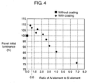
- FIG. 4 is a characteristic chart showing the relationship between the initial luminance and the Al/Si ratio of the PDP device.
- the initial luminance can be increased compared to the phosphor material without coating where the Al/Si ratio is in the range of 0.6 to 2.2.
- the initial luminance decreases with the Al/Si ratio exceeding 2.2.
- the Al/Si ratio is 4.0 or less, the decrease of the initial luminance is about 15% and there is practically no problem.
Landscapes
- Chemical & Material Sciences (AREA)
- Engineering & Computer Science (AREA)
- Physics & Mathematics (AREA)
- Plasma & Fusion (AREA)
- Inorganic Chemistry (AREA)
- Materials Engineering (AREA)
- Organic Chemistry (AREA)
- Luminescent Compositions (AREA)
- Gas-Filled Discharge Tubes (AREA)
Applications Claiming Priority (2)
| Application Number | Priority Date | Filing Date | Title |
|---|---|---|---|
| JP2006046569 | 2006-02-23 | ||
| PCT/JP2007/053017 WO2007097296A1 (fr) | 2006-02-23 | 2007-02-20 | Dispositif d'affichage à plasma et procédé de fabrication de phosphore vert pour ledit dispositif d'affichage |
Publications (2)
| Publication Number | Publication Date |
|---|---|
| EP1860676A1 true EP1860676A1 (fr) | 2007-11-28 |
| EP1860676A4 EP1860676A4 (fr) | 2010-07-14 |
Family
ID=38437336
Family Applications (1)
| Application Number | Title | Priority Date | Filing Date |
|---|---|---|---|
| EP07714543A Withdrawn EP1860676A4 (fr) | 2006-02-23 | 2007-02-20 | Dispositif d'affichage à plasma et procédé de fabrication de phosphore vert pour ledit dispositif d'affichage |
Country Status (6)
| Country | Link |
|---|---|
| US (1) | US7911139B2 (fr) |
| EP (1) | EP1860676A4 (fr) |
| JP (1) | JP4569631B2 (fr) |
| KR (1) | KR100901948B1 (fr) |
| CN (1) | CN101322214B (fr) |
| WO (1) | WO2007097296A1 (fr) |
Families Citing this family (1)
| Publication number | Priority date | Publication date | Assignee | Title |
|---|---|---|---|---|
| JP2010146741A (ja) * | 2008-12-16 | 2010-07-01 | Hitachi Plasma Display Ltd | プラズマディスプレイパネル |
Family Cites Families (16)
| Publication number | Priority date | Publication date | Assignee | Title |
|---|---|---|---|---|
| US4320418A (en) * | 1978-12-08 | 1982-03-16 | Pavliscak Thomas J | Large area display |
| US5196234A (en) * | 1986-08-29 | 1993-03-23 | Gte Products Corporation | Method for preparing zinc orthosilicate phosphor particle |
| US4892757A (en) * | 1988-12-22 | 1990-01-09 | Gte Products Corporation | Method for a producing manganese activated zinc silicate phosphor |
| US4946707A (en) * | 1989-07-28 | 1990-08-07 | Gte Products Corporation | Method for producing an aluminum oxide coated manganese activated zinc silicate phosphor |
| JP2653576B2 (ja) | 1990-08-31 | 1997-09-17 | 株式会社東芝 | 低圧水銀蒸気放電ランプ |
| US5289081A (en) * | 1990-11-28 | 1994-02-22 | Kabushiki Kaisha Toshiba | Fluorescent lamp with phosphor having coated phosphor particles |
| JPH10195428A (ja) * | 1997-01-16 | 1998-07-28 | Toshiba Corp | 蛍光体粒子、その製造方法およびプラズマディスプレイパネル |
| JP3587661B2 (ja) | 1997-09-12 | 2004-11-10 | 富士通株式会社 | プラズマディスプレイパネル |
| US6547617B1 (en) * | 1998-07-08 | 2003-04-15 | Hiroyuki Kawamura | Plasma display panel manufacturing method for manufacturing a plasma display panel with superior picture quality, a manufacturing apparatus and a phosphor ink |
| DE19851348A1 (de) | 1998-11-06 | 2000-05-25 | Philips Corp Intellectual Pty | Lumineszierender Schirm mit oxidhaltiger Leuchtstoffzubereitung |
| TW533447B (en) | 1999-12-14 | 2003-05-21 | Matsushita Electric Industrial Co Ltd | Plasma display apparatus |
| JP2003183650A (ja) | 2001-12-25 | 2003-07-03 | Matsushita Electric Ind Co Ltd | プラズマディスプレイ装置の製造方法 |
| KR100511757B1 (ko) * | 2003-02-19 | 2005-09-01 | 유재수 | 금속산화물이 코팅된 플라즈마 디스플레이 패널용 형광체의 제조방법 및 그로 제조된 플라즈마 디스플레이 패널용 형광체 |
| JP4534563B2 (ja) | 2004-04-13 | 2010-09-01 | パナソニック株式会社 | プラズマディスプレイパネルおよびその製造方法 |
| JP4977331B2 (ja) * | 2004-05-26 | 2012-07-18 | パナソニック株式会社 | 蛍光体およびガス放電表示デバイス |
| US7270774B2 (en) * | 2004-05-26 | 2007-09-18 | Matsushita Electric Industrial Co., Ltd. | Phosphor having resistance to deterioration caused by ultraviolet rays, and gas discharge display device of which image quality is not readily deteriorated over time |
-
2007
- 2007-02-20 CN CN2007800004335A patent/CN101322214B/zh not_active Expired - Fee Related
- 2007-02-20 EP EP07714543A patent/EP1860676A4/fr not_active Withdrawn
- 2007-02-20 WO PCT/JP2007/053017 patent/WO2007097296A1/fr not_active Ceased
- 2007-02-20 JP JP2007528111A patent/JP4569631B2/ja not_active Expired - Fee Related
- 2007-02-20 KR KR1020077018816A patent/KR100901948B1/ko not_active Expired - Fee Related
- 2007-02-20 US US11/886,685 patent/US7911139B2/en not_active Expired - Fee Related
Also Published As
| Publication number | Publication date |
|---|---|
| US20090026949A1 (en) | 2009-01-29 |
| KR100901948B1 (ko) | 2009-06-10 |
| WO2007097296A1 (fr) | 2007-08-30 |
| EP1860676A4 (fr) | 2010-07-14 |
| CN101322214B (zh) | 2010-06-02 |
| US7911139B2 (en) | 2011-03-22 |
| KR20070101331A (ko) | 2007-10-16 |
| JP4569631B2 (ja) | 2010-10-27 |
| CN101322214A (zh) | 2008-12-10 |
| JPWO2007097296A1 (ja) | 2009-07-16 |
Similar Documents
| Publication | Publication Date | Title |
|---|---|---|
| JP2004323576A (ja) | 蛍光体およびプラズマディスプレイ装置 | |
| EP1865528B1 (fr) | Dispositif d'affichage à plasma et procédé de fabrication de phosphore vert pour ledit dispositif d'affichage | |
| EP1865529B1 (fr) | Écran plasma et procédé de fabrication d'un phosphore vert pour écran plasma | |
| EP1903088B1 (fr) | Luminophore vert et écran à plasma le comprenant | |
| US7911139B2 (en) | Plasma display device with improved luminance | |
| EP1890311B1 (fr) | Dispositif d'affichage a plasma | |
| JP2009218021A (ja) | プラズマディスプレイパネル | |
| US20130069521A1 (en) | Plasma-display panel |
Legal Events
| Date | Code | Title | Description |
|---|---|---|---|
| PUAI | Public reference made under article 153(3) epc to a published international application that has entered the european phase |
Free format text: ORIGINAL CODE: 0009012 |
|
| 17P | Request for examination filed |
Effective date: 20070726 |
|
| AK | Designated contracting states |
Kind code of ref document: A1 Designated state(s): AT BE BG CH CY CZ DE DK EE ES FI FR GB GR HU IE IS IT LI LT LU LV MC NL PL PT RO SE SI SK TR |
|
| AX | Request for extension of the european patent |
Extension state: AL BA HR MK YU |
|
| DAX | Request for extension of the european patent (deleted) | ||
| RAP1 | Party data changed (applicant data changed or rights of an application transferred) |
Owner name: PANASONIC CORPORATION |
|
| DAX | Request for extension of the european patent (deleted) | ||
| RBV | Designated contracting states (corrected) |
Designated state(s): DE FR GB NL |
|
| A4 | Supplementary search report drawn up and despatched |
Effective date: 20100614 |
|
| RIN1 | Information on inventor provided before grant (corrected) |
Inventor name: MIYAMAE, YUICHIRO Inventor name: SHIGETOH, NOBUYUKI Inventor name: HORIKAWA, KEIJI Inventor name: SUGIMOTO, KAZUHIKO Inventor name: HIBINO, JUNICHI Inventor name: TOYODA, IZUMI Inventor name: NAGASAKI, YOSHIHISA |
|
| RIC1 | Information provided on ipc code assigned before grant |
Ipc: C09K 11/59 20060101AFI20121129BHEP Ipc: H01J 11/12 20120101ALI20121129BHEP Ipc: H01J 11/42 20120101ALI20121129BHEP |
|
| GRAP | Despatch of communication of intention to grant a patent |
Free format text: ORIGINAL CODE: EPIDOSNIGR1 |
|
| RIN1 | Information on inventor provided before grant (corrected) |
Inventor name: SUGIMOTO, KAZUHIKO Inventor name: MIYAMAE, YUICHIRO Inventor name: TOYODA, IZUMI Inventor name: NAGASAKI, YOSHIHISA Inventor name: HIBINO, JUNICHI Inventor name: HORIKAWA, KEIJI Inventor name: SHIGETOH, NOBUYUKI |
|
| STAA | Information on the status of an ep patent application or granted ep patent |
Free format text: STATUS: THE APPLICATION IS DEEMED TO BE WITHDRAWN |
|
| 18D | Application deemed to be withdrawn |
Effective date: 20130518 |