EP1860919A1 - Élément d électroluminescence et appareil d éclairage - Google Patents
Élément d électroluminescence et appareil d éclairage Download PDFInfo
- Publication number
- EP1860919A1 EP1860919A1 EP06715081A EP06715081A EP1860919A1 EP 1860919 A1 EP1860919 A1 EP 1860919A1 EP 06715081 A EP06715081 A EP 06715081A EP 06715081 A EP06715081 A EP 06715081A EP 1860919 A1 EP1860919 A1 EP 1860919A1
- Authority
- EP
- European Patent Office
- Prior art keywords
- layer
- light
- refractive
- scattering
- index
- Prior art date
- Legal status (The legal status is an assumption and is not a legal conclusion. Google has not performed a legal analysis and makes no representation as to the accuracy of the status listed.)
- Granted
Links
Images
Classifications
-
- G—PHYSICS
- G02—OPTICS
- G02B—OPTICAL ELEMENTS, SYSTEMS OR APPARATUS
- G02B6/00—Light guides; Structural details of arrangements comprising light guides and other optical elements, e.g. couplings
- G02B6/0001—Light guides; Structural details of arrangements comprising light guides and other optical elements, e.g. couplings specially adapted for lighting devices or systems
- G02B6/0011—Light guides; Structural details of arrangements comprising light guides and other optical elements, e.g. couplings specially adapted for lighting devices or systems the light guides being planar or of plate-like form
- G02B6/0033—Means for improving the coupling-out of light from the light guide
- G02B6/005—Means for improving the coupling-out of light from the light guide provided by one optical element, or plurality thereof, placed on the light output side of the light guide
- G02B6/0051—Diffusing sheet or layer
-
- B—PERFORMING OPERATIONS; TRANSPORTING
- B82—NANOTECHNOLOGY
- B82Y—SPECIFIC USES OR APPLICATIONS OF NANOSTRUCTURES; MEASUREMENT OR ANALYSIS OF NANOSTRUCTURES; MANUFACTURE OR TREATMENT OF NANOSTRUCTURES
- B82Y20/00—Nanooptics, e.g. quantum optics or photonic crystals
-
- B—PERFORMING OPERATIONS; TRANSPORTING
- B82—NANOTECHNOLOGY
- B82Y—SPECIFIC USES OR APPLICATIONS OF NANOSTRUCTURES; MEASUREMENT OR ANALYSIS OF NANOSTRUCTURES; MANUFACTURE OR TREATMENT OF NANOSTRUCTURES
- B82Y30/00—Nanotechnology for materials or surface science, e.g. nanocomposites
-
- H—ELECTRICITY
- H05—ELECTRIC TECHNIQUES NOT OTHERWISE PROVIDED FOR
- H05B—ELECTRIC HEATING; ELECTRIC LIGHT SOURCES NOT OTHERWISE PROVIDED FOR; CIRCUIT ARRANGEMENTS FOR ELECTRIC LIGHT SOURCES, IN GENERAL
- H05B33/00—Electroluminescent light sources
- H05B33/02—Details
-
- H—ELECTRICITY
- H10—SEMICONDUCTOR DEVICES; ELECTRIC SOLID-STATE DEVICES NOT OTHERWISE PROVIDED FOR
- H10K—ORGANIC ELECTRIC SOLID-STATE DEVICES
- H10K50/00—Organic light-emitting devices
- H10K50/80—Constructional details
- H10K50/85—Arrangements for extracting light from the devices
- H10K50/854—Arrangements for extracting light from the devices comprising scattering means
-
- H—ELECTRICITY
- H10—SEMICONDUCTOR DEVICES; ELECTRIC SOLID-STATE DEVICES NOT OTHERWISE PROVIDED FOR
- H10K—ORGANIC ELECTRIC SOLID-STATE DEVICES
- H10K50/00—Organic light-emitting devices
- H10K50/80—Constructional details
- H10K50/85—Arrangements for extracting light from the devices
- H10K50/858—Arrangements for extracting light from the devices comprising refractive means, e.g. lenses
-
- H—ELECTRICITY
- H10—SEMICONDUCTOR DEVICES; ELECTRIC SOLID-STATE DEVICES NOT OTHERWISE PROVIDED FOR
- H10K—ORGANIC ELECTRIC SOLID-STATE DEVICES
- H10K59/00—Integrated devices, or assemblies of multiple devices, comprising at least one organic light-emitting element covered by group H10K50/00
- H10K59/80—Constructional details
- H10K59/875—Arrangements for extracting light from the devices
- H10K59/877—Arrangements for extracting light from the devices comprising scattering means
-
- H—ELECTRICITY
- H10—SEMICONDUCTOR DEVICES; ELECTRIC SOLID-STATE DEVICES NOT OTHERWISE PROVIDED FOR
- H10K—ORGANIC ELECTRIC SOLID-STATE DEVICES
- H10K59/00—Integrated devices, or assemblies of multiple devices, comprising at least one organic light-emitting element covered by group H10K50/00
- H10K59/80—Constructional details
- H10K59/875—Arrangements for extracting light from the devices
- H10K59/879—Arrangements for extracting light from the devices comprising refractive means, e.g. lenses
-
- G—PHYSICS
- G02—OPTICS
- G02B—OPTICAL ELEMENTS, SYSTEMS OR APPARATUS
- G02B5/00—Optical elements other than lenses
- G02B5/02—Diffusing elements; Afocal elements
-
- H—ELECTRICITY
- H10—SEMICONDUCTOR DEVICES; ELECTRIC SOLID-STATE DEVICES NOT OTHERWISE PROVIDED FOR
- H10K—ORGANIC ELECTRIC SOLID-STATE DEVICES
- H10K2102/00—Constructional details relating to the organic devices covered by this subclass
- H10K2102/301—Details of OLEDs
- H10K2102/331—Nanoparticles used in non-emissive layers, e.g. in packaging layer
Definitions
- the present invention relates to electroluminescent elements, and in particular, to an electroluminescent element excellent in terms of the light emission efficiency.
- the present invention also relates to a lighting apparatus having the electroluminescent element as its light source.
- electroluminescent elements used in electroluminescent displays and electroluminescent lighting apparatuses emit light on the basis of the principle of recombination of positive holes injected from an anode and electrons injected from a cathode in an electroluminescent layer and subsequent excitation of the luminescence center caused by the recombination energy.
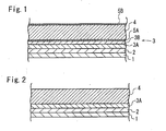
- FIG. 2 is a schematic sectional view of a known general electroluminescent element, wherein an electrode (cathode) 1, an electroluminescent layer 2, a transparent electrode layer (anode) 3A and a translucent body (transparent substrate) are sequentially laminated.
- the light generated in the electroluminescent layer is emitted with a high efficiency.
- the light emitted at an angle close to the critical angle included in the generated light is totally reflected by the interface between the light-emitting surface, i.e., the transparent substrate, and air, and thus becomes guided light (substrate mode) that travels inside the transparent substrate in the planar direction while being totally reflected.
- guided light substrate mode
- other guided light thin film mode
- Patent Document 1 discloses an organic electroluminescent apparatus that has a light-scattering portion formed of a lens sheet in its transparent substrate or has a matt substrate, as a technique for reducing the amount of these kinds of guided light.
- this technique can reduce the amount of the guided light traveling inside the translucent body in the planar direction while being totally reflected by the interface between the translucent body and air
- the other guided light which travels inside the transparent electrode layer or the transparent electrode and electroluminescent layers in the planar direction while being totally reflected by the interface between the transparent electrode layer and the transparent substrate, can not be output, thus reducing the light emission efficiency.
- Patent Document 2 discloses an information display wherein frustrating elements are provided in order to eliminate the internal total reflection of light.
- the frustrating elements that contain bulky diffusing material and are placed at several sites within the device can slightly improve the light emission efficiency, but potential contact between the textured interface and the transparent electrode would cause a lot of problematic dark spots, which may also shorten the life of the element, to form on the light-emitting surface.
- the guided light that travels inside the transparent electrode layer or the transparent electrode and electroluminescent layers in the planar direction while being totally reflected by the interface between the transparent electrode layer and the transparent substrate can not be output, thus reducing the light emission efficiency, just like the technique described in Patent Document 1.
- Patent Document 1 Japanese Patent No. 2931211
- Patent Document 2 PCT Japanese Translation Patent Publication No. 2004-513483
- the present invention provides electroluminescent elements, wherein an electrode, an electroluminescent layer, a high-refractive-index layer and a translucent body are sequentially laminated; the amount of guided light that travels inside the high-refractive-index layer or the high-refractive-index and electroluminescent layers in the planar direction while being totally reflected by the interface between the high-refractive-index layer and the translucent body is reduced as well as guided light that travels inside the translucent body in the planar direction while being totally reflected by the interface between the translucent body and air; and thereby the efficiency with which light is emitted from the electroluminescent element is improved.
- This invention provides, in particular, an electroluminescent element in which decrease in brightness at the edge of image elements, which are required in a lighting apparatus using an electroluminescent element as its light source, can be avoided and directed light can be output.
- Another object of the present invention is to offer a lighting apparatus using such an electroluminescent element as its light source.
- the electroluminescent element of the first aspect is an electroluminescent element, wherein an electrode, an electroluminescent layer, a high-refractive-index layer and a translucent body are sequentially laminated, and on the light-emitting-surface side of each of the high-refractive-index layer and the translucent body, a layer having a light-scattering function is provided.
- the lighting apparatus of the second aspect is a lighting apparatus using the electroluminescent element of the first aspect as its light source.
- the provided layers having the light-scattering function on the light-emitting-surface side of the high-refractive-index layer and the translucent body may realize multiple scattering of guided light that travels inside the translucent body in the planar direction while being totally reflected by the interface between the translucent body and air, and other guided light that travels inside a thin film containing the electroluminescent layer and the high-refractive-index layer, thereby making it possible to emit light from the electroluminescent element.
- the electroluminescent element of the present invention offers the following effects i) to vi).
- the electroluminescent element of the present invention offers brighter light with a smaller amount of the current, thereby providing long-life elements.
- the high brightness obtained also makes it possible to use the electroluminescent elements as light emitters in displays, lighting apparatuses and other applications.
- the electroluminescent element of the present invention can reduce the decrease in brightness at the edge of image elements and emit directed light, and thus is the most suitable for lighting applications.
- the electroluminescent element of the present invention spontaneously emits light and thus can be used in field emission displays and plasma displays having a translucent body. Therefore, the industrial applicability of these elements is very high.
- Embodiments of the electroluminescent element and the lighting apparatus according to the present invention are described in detail below.
- the following statement of configuration requirements is an example (representative example) of embodiments of the present invention, so that this invention is not limited to these embodiments as long as they fall within the scope of the invention.
- a configuration of the electroluminescent element according to the present invention is described below with reference to FIG. 1.
- FIG. 1 is a schematic sectional view of the electroluminescent element according to the embodiment of the present invention.
- an electrode 1 an electroluminescent layer 2, a high-refractive-index layer 3 and a translucent body 4 are sequentially laminated and on the light-emitting-surface side of the high-refractive-index layer 3 and the translucent body 4, layers 5A and 5B having a light-scattering function are provided respectively.
- the electroluminescent element of the present invention may have any other layers between the individual component layers unless the effects of the present invention are impaired.
- the electrode 1 serves as a cathode.
- Preferred material used as the cathode is metal having a low work function or a compound thereof.
- the cathode is typically formed of aluminum, tin, magnesium, indium, calcium, gold, silver, copper, nickel, chrome, palladium, platinum, a magnesium-silver alloy, a magnesium-indium alloy, an aluminum-lithium alloy or other material, with more preferred material being aluminum.
- Thickness of the cathode is not particularly limited, but typically 10 nm or more, preferably 30 nm or more, and more preferably 50 nm or more, and at the same time, typically 1000 nm or less, preferably 500 nm or less, and more preferably 300 nm or less.
- the cathode can be obtained by a vacuum film-forming process, such as vapor deposition and sputtering.
- Laminating a layer of metal having a high work function and being stable in air on the side other than the electroluminescent layer side for the purpose of protecting the cathode formed of metal having a low work function is an effective approach to improve the stability of the element.
- aluminum, silver, copper, nickel, chrome, gold, platinum and other metals are used.
- inserting an ultrathin insulating film (film thickness 0.1 to 5 nm) of LiF, MgF 2 , Li 2 O or other compounds between the cathode and the electroluminescent layer can improve the efficiency of the element.
- cathode is formed of transparent electrode material such as indium oxide and zinc oxide containing indium, and light is emitted from the cathode side may be employed.
- the light-emitting-surface sides of high-refractive-index layer and the translucent body are located at the cathode side.
- the electroluminescent layer 2 is formed of film(s) of material that emits light when receiving a voltage, and may include one or more films having different functions. Examples of the films include a hole-injecting layer, a hole-transporting layer, a light-emitting layer, an electron-transporting layer and an electron-injecting layer.
- Material used in the electroluminescent layer may be commonly used electroluminescent material, e.g., known inorganic electroluminescent material such as activated zinc oxide ZnS:X (X is Mn, Tb, Cu, Sm or other activator elements), CaS: Eu, SrS:Ce, SrGa 2 S 4 :Ce, CaGa 2 S 4 :Ce, CaS:Pb and BaAl 2 S 4 :Eu; organic electroluminescent material classified into low-molecular-weight dyes such as aluminum complexes of 8-hydroxyquinoline, aromatic amines and anthracene single crystals; and organic electroluminescent material classified into conjugated polymer such as poly(p-phenylenevinylene), poly[2-methoxy-5-(2-ethylhexyloxy-1,4-phenylenevinylene], poly(3-alkylthiophene) and polyvinylcarbazole, but not limited to those described above. Besides these light-emitting
- Thickness of the electroluminescent layer 2 is typically 10 nm or more, preferably 30 nm or more, and more preferably 50 nm or more, and at the same time, typically 1000 nm or less, preferably 500 nm or less, and more preferably 200 nm or less.
- the electroluminescent layer 2 can be formed by a vacuum film-forming process such as by vapor deposition and sputtering, or by an application process using chloroform or other compounds as solvent.
- the high-refractive-index layer 3 in the present invention is provided in order to output guided light traveling inside the thin film including the electroluminescent layer 2 in the planar direction, and its refractive index is typically 1.55 or higher, preferably 1.6 or higher, more preferably 1.7 or higher, even more preferably 1.9 or higher and most preferably 2.0 or higher, and at the same time, typically 2.5 or lower and preferably 2.2 or lower.
- the high-refractive-index layer may be formed of two or more layers, and in such a case the refractive index represents the mean value calculated from all the layers included. It should be noted that the refractive index in the present invention is measured using a spectral ellipsometer (wavelength: 350 to 900 nm), except for cases using a prism coupler for samples difficult to measure and analyze.
- the high-refractive-index layer 3 includes at least a transparent electrode layer 3A.
- the high-refractive-index layer 3 may consist of only the single transparent electrode layer 3A or may be a combined layer of the transparent electrode layer 3A and an intermediate layer 3B having a comparable refractive index as shown in FIG. 1.
- the high-refractive-index layer 3 preferably consists of the transparent electrode layer 3A and the intermediate layer 3B having a comparable refractive index since guided light traveling inside the thin film including the electroluminescent layer 2 should be transferred to also the high-refractive-index layer 3.
- the term "comparative refractive index” means a refractive index differing from the other by less than 0.3, preferably by 0.2 or less, more preferably by 0.1 or less, and most preferably by 0.02 or less.
- Thickness of the high-refractive-index layer 3 is typically 200 nm or more and preferably 600 nm or more, and at the same time, typically 100 ⁇ m or less, preferably 50 ⁇ m or less, and more preferably 10 ⁇ m or less. Thickness smaller than 200 nm makes it difficult to control the interface between the transparent electrode layer 3A and the intermediate layer 3B, thereby possibly resulting in black spot formation during light emission and a short life of the element. On the other hand, thickness larger than 50 ⁇ m may reduce transmittance or may cause light to leak. Therefore, the high-refractive-index layer 3 has only a sufficient thickness to achieve appropriate surface smoothness described below.
- a surface (transparent-electrode-layer side) of the high-refractive-index layer is preferably smooth, and its surface roughness Ra is preferably 80 nm or less, more preferably 50 nm or less, and most preferably 30 nm or less.
- the surface roughness Ra larger than 80 nm may cause black spot formation during electroluminescent light emission and a short life of the element.
- the surface roughness Ra of the high-refractive-index layer 3 can be observed using a contact surface profiler (KLB-Tencor Corporation).
- the transparent electrode layer 3A usually acts as an anode of the electroluminescent element.
- a thin film formed of indium oxide containing tin (commonly called ITO), zinc oxide containing aluminum (commonly called AZO), zinc oxide containing indium (commonly called IZO) or other types of combined oxides is preferably used.
- ITO indium oxide containing tin
- AZO zinc oxide containing aluminum
- IZO zinc oxide containing indium
- ITO is the most preferable one.
- the larger transmittance for parallel lights having visible wavelength the better, and the parallel light transmittance is typically 50% or more, preferably 60% or more, and more preferably 70% or more.
- the smaller electrical resistance as surface resistance of the transparent electrode layer 3A the better, and the surface resistance is typically 1 to 100 ⁇ / ⁇ ( 1 cm 2 ). Its upper limit is preferably 70 ⁇ / ⁇ , and more preferably 50 ⁇ / ⁇ .
- Thickness of the transparent electrode layer 3A is typically 0.01 to 10 ⁇ m as far as the layer meets the abovementioned requirements for light transmittance and surface resistance. Considering the conductivity, however, the thickness is preferably 0.03 ⁇ m or more, and more preferably 0.05 ⁇ m or more. On the other hand, the thickness is preferably 1 ⁇ m or less, and more preferably 0.5 ⁇ m or less from the perspective of ensuring the light transmittance.
- a coating agent used to form the transparent electrode layer 3A examples include, but are not limited to, a dispersion fluid prepared by mixing ITO fine particles and conductive polymer or other resin binders with organic medium, and conductive polymer material.
- the transparent electrode layer 3A is formed into a pattern required for an electrode of the electroluminescent element by using such a coating agent via photolithography, ink-jet printing or other techniques.
- the standard width of each patterned line is 1 to 10 ⁇ m, but not limited to this range.
- Intermediate layer having a refractive index comparable with that of the transparent electrode layer (hereinafter, abbreviated to an intermediate layer)
- the intermediate layer 3B may be formed on either the light-emitting-surface side, as shown in FIG. 1, or the electroluminescent-layer 2 side of the transparent electrode layer 3A, or otherwise, two layers may be formed on both sides. Formed on the light-emitting-surface side of the transparent electrode layer 3A, the intermediate layer 3B preferably has insulation properties. Formed on the electroluminescent-layer 2 side, the intermediate layer 3B preferably has conductivity. It should be noted that, in a more preferable configuration, the intermediate layer 3B having insulating properties is formed on the light-emitting-surface side of the transparent electrode layer 3A.
- the intermediate layer 3B is a film formed by the sol-gel reaction or vacuum processes, and examples of its material include inorganic oxide material such as SiN x O y (x and y are positive integers or zero), TiO 2 , ZrO 2 and zeolite, organic material such as thermosetting resins, UV-curable resins and conductive resins, as well as composite material thereof.
- the intermediate layer 3B may be a laminated product of these materials.
- Material of the intermediate layer 3B is not particularly limited, but may be material that has a refractive index adjusted in advance by dispersing fine particles of high-refractive-index compounds such as TiO 2 Al 2 O 3 , ZrO 2 and Ta 2 O 3 in a matrix such as resin or silicate, since the layer should be similar to the transparent electrode layer 3A in terms of the refractive index.
- One or more kinds of the fine particles may be used.
- the resin constituting the matrix include polyethylene, polypropylene, polyethylene terephthalate, polymethyl methacrylate, polystyrene, polyethersulfone, polyarylate, polycarbonate resins, polyurethane, acryl resins, polyacrylonitrile, polyvinyl acetal, polyamide, polyimide, diacrylphthalate resins, cellulose resins, polyvinyl chloride, polyvinylidene chloride, polyvinyl acetate and other thermoplastic resins, as well as copolymer containing two or more kinds of monomers of the resins described above.
- the intermediate layer 3B should have a refractive index comparable with that of the transparent electrode layer 3A and a differential refractive index of 0.3 or more may result in insufficient emission of guided light from the thin film including the electroluminescent layer 2. Therefore, it is important that the difference in refractive index between the transparent electrode layer 3A and the intermediate layer 3B is less than 0.3, preferably 0.2 or less, more preferably 0.1 or less, and most preferably 0.02 or less.
- Thickness of the intermediate layer 3B is typically 250 nm or more, preferably 600 nm or more, and at the same time, typically 50 ⁇ m or less and preferably 10 ⁇ m or less.
- the intermediate layer 3B can be usually obtained by an application process such as spin-coating, dip-coating and die-coating, or a vacuum process such as vapor deposition and sputtering.
- a surface of the intermediate layer is preferably smooth, and its surface roughness Ra is preferably 100 nm or less, more preferably 50 nm or less, and most preferably 10 nm or less.
- the surface roughness larger than 100 nm may result in black spot formation during electroluminescent light emission and a short life of the element.
- the surface roughness Ra of the intermediate layer 3B can be observed using a contact surface profiler (KLB-Tencor Corporation).
- the high-refractive-index layer 3 includes both the transparent electrode layer 3A and the intermediate layer 3B having a refractive index comparable with that of the transparent electrode layer 3A
- a part of the high-refractive-index layer 3, e.g., the intermediate layer 3B, or the entire high-refractive-index layer 3 chemically reacts with the transparent electrode layer 3A, thereby possibly resulting in black spot formation during electroluminescent light emission and a short life of the element. Therefore, it is preferable that a gas barrier layer is present between the transparent electrode layer 3A and the intermediate layer 3B.
- Examples of material used to form the gas barrier layer include, but not limited to, ZrC 2 , TiO 2 , Al 2 O 3 , CeO 2 , TiN, Ta 2 O 5 , SiO x N y , SiN, SiO x , SnO 2 , Sb 2 O 5 , Y 2 O 3 , La 2 O 3 and In 2 O 3 , and mixture thereof. Any material that shows no absorbance in a visible wavelength region or at least has a dense structure when formed into a film may be used, and the main ingredient of the material is preferably an inorganic compound.
- thickness of the gas barrier layer is not particularly limited, considering the barrier properties, the thickness is typically 5 nm or more, preferably 20 nm or more, more preferably 50 nm or more, and most preferably 100 nm or more, and at the same time, typically 10 ⁇ m or less, preferably 1 ⁇ m or less, and more preferably 400 nm or less.
- a gas barrier layer that contains inorganic material and has a thickness of 5 nm to 400 nm, and preferably 10 nm to 300 nm, more specifically, approximately 30 nm.
- This gas barrier layer is formed by a vacuum process such as vapor deposition and sputtering.
- the refractive index of the gas barrier layer is preferably comparable with that of the transparent electrode layer 3A, but low-refractive-index material may also be used as far as the film thickness is 200 nm or less. Examples of such a low-refractive-index material include fluoride such as MgF 2 , NaF 2 and NaF 2 , and nanoporous materials.
- the translucent body 4 is usually used as a substrate of the electroluminescent element.
- the translucent body 4 has a refractive index comparable with or greater than that of the high-refractive-index layer 3, and its refractive index is typically 1.4 or more, preferably 1.45 or more, more preferably 1.47 or more, while being less than 1.9, preferably less than 1.80, and more preferably less than 1.75, but is not particularly limited.
- the refractive index of the translucent body 4 is determined using optical means such as an ellipsometer, reflection meter and prism coupler.
- a transparent substrate formed of commonly used material may be used as the translucent body 4 having such a refractive index.
- the transparent substrate include a wide variety of Schott glass such as BK 7 , SF 11 , LaSFN 9 , BaK 1 and F 2 ; glass such as synthetic fused silica glass, optical crown glass, low-expansion borosilicate glass, sapphire glass, soda glass and non-alkali glass; acryl resins such as polymethyl methacrylate and crosslinked acrylate; aromatic polycarbonate resins such as bisphenol A polycarbonate; polyester resins such as polyethylene terephthalate; amorphous polyolefin resin such as polycycloolefin; epoxy resins; styrene resins such as polystyrene; polysulfone resins such as polyethersulfone; and synthetic resins such as polyetherimide resin, as well as a laminated product thereof.
- Schott glass such as BK 7 , SF 11 , LaS
- Schott glass synthetic fused silica glass, optical crown glass, low-expansion borosilicate glass, soda glass, non-alkali glass, acryl resins, aromatic polycarbonate resins and polysulfone resins are preferred.
- an optical film such as an antireflection film, a circular polarizing film or a phase difference film may be formed or laminated depending on its purpose and application.
- Thickness of the translucent body 4 is typically 0.1 mm to 10 mm. Considering the mechanical integrity and gas barrier properties, the thickness is preferably 0.2 mm or more. On the other hand, the thickness is preferably 5 mm or less, and more preferably 3 mm or less from the perspective of reducing the weight and ensuring the light transmittance.
- the translucent body 4 is preferably a transparent substrate, but a top-emitting device configuration wherein a protective cover instead of the transparent substrate is mounted on the high-refractive-index layer may also be used. In this configuration, it is advisable that the translucent body 4 acts as the protective cover.
- Material of the protective cover is not particularly limited as far as it is transparent, and thus examples of the material include a wide variety of resin material such as hardening resins and coating material such as sol-gel films.
- layers having a light-scattering function 5A and 5B are provided.
- the light-scattering function means a capability of multiple scattering of emitted light using Mie scattering.
- This light-scattering function makes it possible to scatter guided light in the thin film including the electroluminescent layer 2 or leaking light of the guided light in the direction of light emission.
- Efficient multiple scattering needs appropriate adjustment of differential refractive index between the scattering body or the scattering shape and the matrix around the scattering body or the scattering shape, as well as the size of the scattering body or the scattering shape.
- the distance between the scattering bodies is preferably comparable with or shorter than the size of each scattering body, and more preferably, 1/2 of or shorter than the size of each scattering body.
- the distance between the scattering bodies is preferably 1/10 of or longer than the wavelength.
- the lengths described above can be determined by surface observation using a scanning electron microscope or a transmission electron microscope, or by an X-ray scattering study.
- the scattering body means transparent particles, described later, and the scattering shape means the shape of the textured interface.
- the matrix particularly means, as for a layer containing the transparent particles, the same matrix as stated in the description of the intermediate layer 3B, and as for the textured interface, it means material, air or others in contact with the textured surface.
- the light-emitting-surface side of each of the high-refractive-index layer 3 and the translucent body 4 is a surface having a refractive index greatly different from that of the adjacent layer, such as the surface of the high-refractive-index layer 3,in contact with the translucent body 4, and the surface of the translucent body in contact with air.
- the layer having the light-scattering function 5B which is formed on the light-emitting-surface side of the translucent body 4, preferably has a refractive index higher than that of the translucent body 4 to emit light in the substrate mode efficiently.
- the preferred differential refractive index between the translucent body 4 and the layer having the light-scattering function 5B is usually 0.02 to 1.5.
- the layers having the light-scattering function 5A and 5B may be layers other than each layer included in the high-refractive-index layer 3 and the translucent body 4, or may be formed by texturing the surface of each layer included in the high-refractive-index layer 3 and the translucent body 4 using blast finishing or other polishing processes. In particular, layers containing transparent particles or irregularly textured interfaces are preferred.
- thickness of each of the layers having the light-scattering function 5A and 5B in the direction of film thickness is preferably 100 nm or more, and more preferably 200 nm or more. A thickness less than 100 nm reduces multiple scattering performance and increases anisotropy of the scattering, thereby possibly causing view-angle dependence of the brightness to occur. Also, the thickness of each of the layers having the light-scattering function 5A and 5B is preferably 50 ⁇ m or less, and more preferably 10 ⁇ m or less. A thickness greater than 50 ⁇ m causes changes in scattering properties to occur during the emitted light travels along a light path inside the layers having the light-scattering function, thereby possibly resulting in the abovementioned view-angle dependence of the brightness.
- a preferred light transmittance of the layers having the light-scattering function 5A and 5B is 90% or lower, a more preferred one is 80% or lower, and the most preferred one is 70% or lower.
- the transmittance is preferably 25% or higher, and more preferably 40% or higher.
- the parallel light transmittance of each of the layers having the light-scattering function 5A and 5B is preferably 30% to 80%.
- This irregularly textured interface means an interface having a nonperiodic and uneven structure, and the surface roughness Ra of the interface is preferably 10 nm or more and more preferably 100 nm or more, in order to reduce total reflection of the emitted light by the interface. Also, considering leakage of the light, the surface roughness Ra is preferably 10 ⁇ m or less, and more preferably 1 ⁇ m or less. Although some advanced rough surface structures, such as photonic crystal-based microlenses, have conventionally been proposed, irregularly textured structure of the interface is important not only for cost-cutting but also for reducing anisotropy of scattering.
- the surface roughness Ra is determined by averaging values measured with 0.5 ⁇ m of scan length using P-15 contact surface profiler, manufactured by KLA-Tencor Corporation, according to the standards specified in JIS B0601:2001.
- the irregularly textured interface that acts as a layer having the light-scattering function can be obtained by blast finishing or other polishing processes, or otherwise can be formed by applying transparent particles on the interface.
- the transparent particles are particles showing no or low absorbance (in general, 30% or lower) in a visible wavelength region, and examples of them include porous substances formed of TiO 2 SiO 2 , ZrO 2 , Al 2 O 3 , Ta 2 O 3 , ZnO 2 , Sb 2 O 3 , ZrSiO 4 , zeolite and combinations thereof, and inorganic particles containing these compounds as the main ingredient, as well as organic particles of acryl resin, styrene resin, polyethylene terephthalate resin and others.
- inorganic particles in particular, those formed of TiO 2 , SiO 2 , porous SiO 2 , ZrO 2 , Al 2 O 3 or zeolite are preferred.
- the transparent particles may be used separately or in combination of two or more kinds.
- the particle size is typically 100 nm or more, preferably 250 nm or more, and more preferably 300 nm or more, and at the same time, typically 20 ⁇ m or less, and preferably 10 ⁇ m or less.
- the particle size is preferably 80 to 700 nm, while in the layer having the light-scattering function 5B the particle size is preferably 150 nm to 8 ⁇ m.
- the differential refractive index between the matrix and the transparent particles serving as the scattering bodies is preferably 0.01 or more, more preferably 0.03 or more, and most preferably 0.05 or more, and at the same time, preferably less than 2, more preferably less than 1.5, and most preferably less than 1.
- the differential refractive index between the matrix and the scattering bodies ⁇ N is preferably -0.3 to 1.5. Moreover, the refractive index of the scattering bodies (N s ) is preferably 1.7 or less.
- the transparent particles serving as scattering bodies and contained in the layer having the light-scattering function 5A located at the light-emitting-surface side of the high-refractive-index layer 3 have a refractive index of 1.6 or more, and preferably 1.8 or more
- the transparent particles serving as scattering bodies and contained in the layer having the light-scattering function 5B located at the light-emitting-surface side of the translucent body 4 preferably have a refractive index of 1.7 or less, and more preferably 1.57 or less, because it is preferable that scattering properties of the transparent particles are different between the layers having the light-scattering function.
- the layer having the light-scattering function formed of a layer containing transparent particles may be laminated layers formed using several kinds of transparent particles and/or matrices.
- the layer containing transparent particles is usually a multiple-light-scattering layer formed by applying a coating agent in which the transparent particles have been dispersed in a matrix precursor.
- the differential refractive index between the matrix and the transparent particles are, as stated above, preferably 0.01 or more, and more preferably 0.03 or more, and most preferably 0.05 or more, and at the same time, preferably less than 2, more preferably less than 1.5, and most preferably less than 1.
- the difference between the refractive index of the matrix and the transparent particles serving as the scattering bodies ⁇ N is preferably - 1.8 to -0.3
- the differential refractive index between the matrix and the scattering bodies ⁇ N is preferably -0.3 to 1.5.
- any kind of matrix precursors may be used depending on the kind of transparent particles to be dispersed therein, and examples of material commonly used as the precursors include sol-gel precursors such as silicate oligomer, reactive precursors such as monomers of thermosetting resins and UV-curable resins, molten resins, or precursors containing these as the main ingredient.
- sol-gel precursors such as silicate oligomer
- reactive precursors such as monomers of thermosetting resins and UV-curable resins
- molten resins or precursors containing these as the main ingredient.
- the content of transparent particles in the coating agent must be adjusted so as to achieve multiple Mie scattering in the transparent particle-containing layer to be formed.
- Examples of methods used to apply such a coating agent include spin-coating, dip-coating, die-coating, casting, spray-coating and gravure-coating. Considering the homogeneity of films, the most preferred method is spin-coating, dip-coating or die-coating.
- the textured interface may be an interface having a random structure formed utilizing the differential refractive index.
- a layer having a refractive index lower than that of the translucent body 4 (hereinafter, a low-refractive-index layer) between the high-refractive-index layer 3 and the translucent body 4 is preferable, in order to emit the generated light, which has been transferred to the high-refractive-index layer 3, from the translucent body 4 with a high efficiency.
- the presence of the low-refractive-index layer can make the emitted light directive.
- a layer that contains silica, fluororesins such as circular Teflon, magnesium fluoride or others and whose refractive index is typically 1.05 or more, and particularly 1.1 or more, and at the same time typically 1.5 or less, preferably 1.35 or less, and more preferably 1.3 or less is suitably used as the low-refractive-index layer, and in particular, a layer containing porous silica is suitable. It is important to ensure that the refractive index of the low-refractive-index layer is smaller than that of the translucent body. However, an excessively low refractive index often leads to an issue concerning the mechanical integrity, while an excessively high-refractive-index reduces the light emission efficiency.
- organic components may be optionally introduced to silica for the purposes such as hydrophobization, softening and prevention of cracks.
- Devices of the top-emitting type can be configured using air (void) as the low-refractive-index layer with no problem. In this case, the refractive index would be 1.0.
- the lighting apparatus according to the present invention uses the electroluminescent element of the present invention as its light source.
- the electroluminescent element according to the present invention has advantages of reducing decrease in brightness at the edge of image elements, making the emitted light directive, and providing light having uniform intensity as a lighting device, thus being useful as a light source of a lighting apparatus.
- the lighting apparatus of the present invention is configured by placing image elements that consist of the electroluminescent elements in front of the subject to be illuminated.
- image elements that consist of the electroluminescent elements
- it is preferably used as a sheet-shaped lighting device.
- a transparent electrode layer is formed on the side other than the light-emitting-surface side of non-alkali glass (refractive index 1.5) manufactured by Asahi Glass Co., Ltd., by sputtering ITO at room temperature so that the film thickness is approximately 100 nm.
- a hole-injecting layer and a hole-transporting layer are formed, and then a light-emitting layer is formed thereon by vapor deposition of tris(8-hydroxyquinolinate)aluminum complex so that the film thickness is approximately 150 nm.
- A1 is vapor-deposited on the light-emitting layer so that the film thickness is approximately 100 nm to complete an organic electroluminescent element.
- the number of black spots having a diameter of 0.5 mm or larger per 5-cm square is three or less.
- the light-emitting-surface side of non-alkali glass manufactured by Asahi Glass Co., Ltd. is used as the translucent body (substrate), on which a precursor coating agent prepared by dispersing silica particles SO-G2 (average particle size 600 nm, refractive index 1.5) manufactured by Admatechs in silicate oligomer (refractive index after curing of the oligomer is 1.5) is spin-coated. Then the coating agent is cured at 250°C to form a light-scattering layer.
- the surface roughness Ra and light transmittance of this light-scattering layer are approximately 200 nm and approximately 50%, respectively.
- a porous silica film to be used as the low-refractive-index layer is formed by casting.
- the film thickness and refractive index of the porous silica film are approximately 830 nm and approximately 1.2, respectively.
- a precursor coating agent prepared by dispersing zirconia particles RC-100 (average particle size 1.9 ⁇ m, refractive index 2.0) manufactured by Daiichi Kigenso Kagaku Kogyo Co., Ltd. in silicate oligomer is spin-coated, and then the coating agent is cured at 250°C to form a light-scattering layer.
- the surface roughness Ra and light transmittance of this light-scattering layer are approximately 350 nm and 50% (by the light-scattering layer only), respectively.
- a coating agent prepared by dispersing titania particles TTO-55D (average particle size 30 nm, refractive index 2.4) manufactured by Ishihara Sangyo Kaisha, Ltd. in UV-curable resin UV1000 monomer (refractive index after curing is 1.6) manufactured by Mitsubishi Chemical Corporation is spin-coated, and then the coating agent is cured by UV irradiation to form a high-refractive-index layer.
- the refractive index, film thickness and surface roughness Ra of this composite layer of titania particles and UV-curable resin are approximately 1.8, approximately 10 ⁇ m and approximately 1 nm, respectively.
- a transparent electrode layer is formed on this composite layer of titania particles and UV-curable resin by sputtering ITO at room temperature so that the film thickness is approximately 100 nm.
- a hole-injecting layer and a hole-transporting layer are formed, and then a light-emitting layer is formed thereon by vapor deposition of tris(8-hydroxyquinolinate)aluminum complex so that the film thickness is approximately 150 nm.
- Al is vapor-deposited on the light-emitting layer so that the film thickness is approximately 100 nm to complete an organic electroluminescent element.
- the initial brightness of the obtained organic electroluminescent element is approximately 2.5-fold when compared with the light emission efficiency in Reference Example 1.
- the number of black spots having a diameter of 0.5 mm or larger per 5-cm square is five or less.
- Non-alkali glass manufactured by Asahi Glass Co., Ltd. is used as the translucent body (transparent substrate), both surfaces of which a precursor coating agent prepared by dispersing silica particles SO-G2 (average particle size 600 nm) manufactured by Admatechs in silicate oligomer is dip-coated. Then the coating agent is cured at 250°C to form light-scattering layers.
- the surface roughness Ra and light transmittance (by one layer only) of these light-scattering layers are considered to be similar to those of Example 1.
- a coating agent prepared by dispersing titania particles TTO-55D (average particle size 30 nm) manufactured by Ishihara Sangyo Kaisha, Ltd. in UV-curable resin UV1000 monomer manufactured by Mitsubishi Chemical Corporation is spin-coated, and then the coating agent is cured to form a high-refractive-index layer.
- the refractive index, film thickness and surface roughness Ra of this composite layer of titania particles and UV-curable resin are approximately 1.8, approximately 7 ⁇ m and approximately 2 nm, respectively.
- a transparent electrode layer is formed on this composite layer of titania particles and UV-curable resin by sputtering ITO at room temperature so that the film thickness is approximately 100 nm.
- a hole-injecting layer and a hole-transporting layer are formed, and then a light-emitting layer is formed thereon by vapor deposition of tris(8-hydroxyquinolinate)aluminum complex so that the film thickness is approximately 150 nm.
- Al is vapor-deposited on the light-emitting layer so that the film thickness is approximately 100 nm to complete an organic electroluminescent element.
- the initial brightness of the obtained organic electroluminescent element is approximately 1.8-fold when compared with the light emission efficiency in Reference Example 1.
- a precursor coating agent prepared by dispersing titania particles TS-01 (average particle size 215 nm, refractive index 2.6) manufactured by Showa Denko K.K. and titania particles TTO-55D (average particle size 30 nm) manufactured by Ishihara Sangyo Kaisha, Ltd. in UV-curable resin UV1000 monomer manufactured by Mitsubishi Chemical Corporation is spin-coated, and then the coating agent is cured by UV irradiation to form a light-scattering layer.
- the refractive index, film thickness and surface roughness Ra of this composite layer of titania particles and UV-curable resin are approximately 1.8, approximately 6 ⁇ m and approximately 1 nm, respectively.
- the light transmittance is approximately 70% (by the light-scattering layer only).
- a transparent electrode layer is formed on this composite layer of titania particles and UV-curable resin by sputtering ITO at room temperature so that the film thickness is approximately 100 nm.
- a hole-injecting layer and a hole-transporting layer are formed, and then a light-emitting layer is formed thereon by vapor deposition of tris(8-hydroxyquinolinate)aluminum complex so that the film thickness is approximately 150 nm.
- A1 is vapor-deposited on the light-emitting layer so that the film thickness is approximately 100 nm to complete an organic electroluminescent element.
- the initial brightness of the obtained organic electroluminescent element is approximately 2.3-fold when compared with the light emission efficiency in Reference Example 1.
- the number of black spots having a diameter of 0.5 mm or larger per 5-cm square is five or less.
- a transparent electrode layer is formed by sputtering ITO at room temperature so that the film thickness is approximately 130 nm.
- a coating hole-injecting layer and a hole-transporting layer PPD: p-phenylenediamine
- PPD p-phenylenediamine
- a light-emitting layer is formed thereon by vapor deposition of tris(8-hydroxyquinolinate)aluminum complex so that the film thickness is 60 nm, thereby forming an electroluminescent layer.
- LiF and Al which are to be used as an electrode (cathode) are vapor-deposited on the electroluminescent layer so that the film thickness is 0.5 nm and 80 nm, respectively, to complete an organic electroluminescent element.
- the light emission efficiency of this element is defined as 1, and is used as the standard for comparison with the elements in Examples 4 to 7 and Comparative Examples 1 and 2 below.
- a precursor coating agent prepared by dispersing rutile titania particles R-61N (average dispersed particle size 250 nm, refractive index 2.6) manufactured by Sakai Chemical Industry Co., Ltd. in UV-curable resin UV1000 monomer manufactured by Mitsubishi Chemical Corporation was spin-coated, and then the coating agent was cured by UV irradiation to form a light-scattering layer.
- the film thickness, refractive index, surface roughness Ra and parallel light transmittance of this light-scattering layer were 3.5 ⁇ m, 1.62, 1.5 nm and 56%, respectively.
- the electroluminescent element was thus completed in the same way as Reference Example 2, except for formation of the light-scattering layers on both sides of the glass substrate.
- a precursor coating agent prepared by dispersing silica particles SO-G5 (average dispersed particle size 530 nm) manufactured by Admatechs in silicate oligomer was dip-coated, and then the coating agent was cured at 150°C for 15 minutes and then at 250°C for 15 minutes to form a light-scattering layer.
- the surface roughness Ra and parallel light transmittance of the light-scattering layer were 355 nm and 54%, respectively.
- a precursor coating agent prepared by dispersing rutile titania particles R-61N (average dispersed particle size 250 nm, refractive index 2.6) manufactured by Sakai Chemical Industry Co., Ltd. in UV-curable resin UV1000 monomer manufactured by Mitsubishi Chemical Corporation was spin-coated, and then the coating agent was cured by UV irradiation to form another light-scattering layer.
- the film thickness, refractive index, surface roughness Ra and parallel light transmittance of this light-scattering layer were 3.5 ⁇ m, 1.62, 1.5 nm and 56%, respectively.
- the electroluminescent element was thus completed in the same way as Reference Example 2, except for formation of the light-scattering layers on both sides of the glass substrate.
- a light-scattering layer was formed in the same way as the layer formed on the light-emitting-surface side of the substrate in Example 5.
- a precursor agent prepared by dissolving Pluronic, triblock copolymer, in partially hydrolyzed alkoxysilane was applied on the other side of the substrate, and then calcined at 450°C to form a porous silica layer.
- the film thickness and refractive index at 550 nm wavelength of this porous silica film were 830 nm and 1.15, respectively, and thus this porous silica film was used as the low-refractive-index layer.
- a precursor coating agent prepared by dispersing rutile titania particles R-61N (average dispersed particle size 250 nm) manufactured by Sakai Chemical Industry Co., Ltd. in UV-curable resin UV1000 monomer manufactured by Mitsubishi Chemical Corporation was spin-coated, and then the coating agent was cured by UV irradiation to form a light-scattering layer.
- the film thickness, refractive index, surface roughness Ra and parallel light transmittance of this light-scattering layer were 3.5 ⁇ m, 1.62, 1.5 nm and 56%, respectively.
- the electroluminescent element was thus completed in the same way as Reference Example 2, except for formation of the two transparent particle-containing layers and the low-refractive-index layer.
- a precursor coating agent prepared by dispersing silica particles SO-G5 (average dispersed particle size 408 nm) manufactured by Admatechs in silicate oligomer was spin-coated, and then the coating agent was cured by UV irradiation to form a light-scattering layer.
- the surface roughness Ra and parallel light transmittance of the light-scattering layer were 61 nm and 54%, respectively.
- a precursor agent prepared by dissolving Pluronic, triblock copolymer, in partially hydrolyzed alkoxysilane was applied on the other side of the substrate, and then calcined at 450°C to form a porous silica layer.
- the film thickness and refractive index at 550 nm wavelength of this porous silica film were 830 nm and 1.15, respectively, and thus this porous silica film was used as the low-refractive-index layer.
- a precursor coating agent prepared by dispersing rutile titania particles R-61N (average dispersed particle size 250 nm) manufactured by Sakai Chemical Industry Co., Ltd. in UV-curable resin UV1000 monomer manufactured by Mitsubishi Chemical Corporation was spin-coated, and then the coating agent was cured by UV irradiation to form a light-scattering layer.
- the film thickness, refractive index, surface roughness Ra and parallel light transmittance of this light-scattering layer were 3.5 ⁇ m, 1.62, 1.5 nm and 56%, respectively.
- the electroluminescent element was thus completed in the same way as Reference Example 2, except for formation of the two transparent particle-containing layers and the low-refractive-index layer.
- the electroluminescent element was completed in the same way as Reference Example 2, except for formation of an additional light-scattering layer on the light-emitting-surface side of the first light-scattering layer by dip-coating of a precursor coating agent prepared by dispersing silica particles SO-G5 (average particle size 408 nm) manufactured by Admatechs in silicate oligomer followed by curing the coating agent at 150°C for 15 minutes and then at 250°C for 15 minutes.
- the surface roughness Ra and parallel light transmittance of the light-scattering layer were 355 nm and 54%, respectively.
- the electroluminescent element was completed in the same way as Reference Example 2, except for formation of a light-scattering layer on the electroluminescent layer side of the non-alkali glass manufactured by Asahi Glass Co., Ltd. by spin-coating of a precursor coating agent prepared by dispersing rutile titania particles R-61N (average dispersed particle size 250 nm) manufactured by Sakai Chemical Industry Co., Ltd. in UV-curable resin UV1000 monomer manufactured by Mitsubishi Chemical Corporation followed by curing the coating agent by UV irradiation.
- the film thickness, refractive index, surface roughness Ra and parallel light transmittance of this light-scattering layer were 3.5 ⁇ m, 1.62, 1.5 nm and 56%, respectively.
- the initial brightness of the obtained organic electroluminescent element was 1.03-fold (evaluation condition 1) and 1.31-fold (evaluation condition 2) when compared with the light emission efficiency in Reference Example 2.
- containment of the guided light traveling inside the substrate resulted in insufficient brightness and inadequate reduction of the decrease in brightness at the edge of elements.
- the electroluminescent element of the present invention proved to be useful as a light source used in a lighting apparatus. It was also revealed that addition of a low-refractive-index layer provides the emitted light with directivity.
Landscapes
- Chemical & Material Sciences (AREA)
- Engineering & Computer Science (AREA)
- Physics & Mathematics (AREA)
- Nanotechnology (AREA)
- Optics & Photonics (AREA)
- Crystallography & Structural Chemistry (AREA)
- General Physics & Mathematics (AREA)
- Composite Materials (AREA)
- Materials Engineering (AREA)
- Condensed Matter Physics & Semiconductors (AREA)
- Life Sciences & Earth Sciences (AREA)
- Biophysics (AREA)
- Electroluminescent Light Sources (AREA)
Applications Claiming Priority (2)
| Application Number | Priority Date | Filing Date | Title |
|---|---|---|---|
| JP2005069487 | 2005-03-11 | ||
| PCT/JP2006/303972 WO2006095632A1 (fr) | 2005-03-11 | 2006-03-02 | Élément d’électroluminescence et appareil d’éclairage |
Publications (3)
| Publication Number | Publication Date |
|---|---|
| EP1860919A1 true EP1860919A1 (fr) | 2007-11-28 |
| EP1860919A4 EP1860919A4 (fr) | 2010-06-30 |
| EP1860919B1 EP1860919B1 (fr) | 2012-02-15 |
Family
ID=36953232
Family Applications (1)
| Application Number | Title | Priority Date | Filing Date |
|---|---|---|---|
| EP06715081A Ceased EP1860919B1 (fr) | 2005-03-11 | 2006-03-02 | Élément d électroluminescence et appareil d éclairage |
Country Status (4)
| Country | Link |
|---|---|
| US (1) | US8125128B2 (fr) |
| EP (1) | EP1860919B1 (fr) |
| TW (1) | TWI389597B (fr) |
| WO (1) | WO2006095632A1 (fr) |
Cited By (19)
| Publication number | Priority date | Publication date | Assignee | Title |
|---|---|---|---|---|
| WO2009007919A3 (fr) * | 2007-07-11 | 2009-02-26 | Koninkl Philips Electronics Nv | Diodes électroluminescentes organiques ayant un meilleur découplage optique |
| GB2448564B (en) * | 2007-11-26 | 2009-04-29 | Iti Scotland Ltd | Light guides |
| WO2009107043A1 (fr) * | 2008-02-27 | 2009-09-03 | Koninklijke Philips Electronics N.V. | Dispositifs optoélectroniques organiques cachés |
| WO2009124532A1 (fr) * | 2008-04-11 | 2009-10-15 | Novaled Ag | Composant organique électro-optique |
| WO2010095514A1 (fr) * | 2009-02-20 | 2010-08-26 | Fujifilm Corporation | Élément optique et dispositif d'affichage à électroluminescence organique muni de l'élément optique |
| DE102009036134A1 (de) * | 2009-08-05 | 2011-02-10 | Schott Ag | Substratglas für Lumineszenzdioden mit einer Streupartikel enthaltenden Schicht und Verfahren zu dessen Herstellung |
| DE102009036135A1 (de) * | 2009-08-05 | 2011-02-10 | Schott Ag | Strukturiertes Substratglas für Lumineszenzdioden und Verfahren zu dessen Herstellung |
| EP2278854A4 (fr) * | 2008-03-26 | 2011-04-13 | Sumitomo Chemical Co | Dispositif électroluminescent organique, dispositif d'éclairage et dispositif d'affichage |
| CN102034846A (zh) * | 2009-09-30 | 2011-04-27 | 统宝光电股份有限公司 | 图像显示系统 |
| EP2249619A4 (fr) * | 2008-01-31 | 2012-05-23 | Sumitomo Chemical Co | Plaque transparente dotée d'un film conducteur transparent et dispositif électroluminescent organique |
| CN103207523A (zh) * | 2012-01-16 | 2013-07-17 | 东洋油墨Sc控股株式会社 | 光散射层用树脂组合物、光散射层、及有机电致发光装置 |
| EP2674442A3 (fr) * | 2012-06-12 | 2014-01-22 | Toyo Ink SC Holdings Co., Ltd. | Composition de résine pour couche de diffusion de lumière, couche de diffusion de lumière et dispositif électroluminescent organique |
| US8686630B2 (en) | 2009-02-09 | 2014-04-01 | Konica Minolta Holdings, Inc. | Organic electroluminescence element and illumination device using the same |
| US9164223B2 (en) | 2009-03-05 | 2015-10-20 | Iti Scotland Limited | Light guides |
| EP2998768A1 (fr) * | 2014-09-19 | 2016-03-23 | NGK Insulators, Ltd. | Composant optique |
| US9625641B2 (en) | 2009-03-05 | 2017-04-18 | Design Led Products Limited | Light guides |
| US9709721B2 (en) | 2008-10-21 | 2017-07-18 | Design Led Products Limited | Light guides |
| US10147894B2 (en) | 2013-05-17 | 2018-12-04 | Saint-Gobain Glass France | Transparent diffusive oled substrate and method for producing such a substrate |
| WO2020181190A1 (fr) * | 2019-03-07 | 2020-09-10 | Vitro Flat Glass Llc | Région d'extraction de lumière de borosilicate |
Families Citing this family (20)
| Publication number | Priority date | Publication date | Assignee | Title |
|---|---|---|---|---|
| JP5536977B2 (ja) * | 2007-03-30 | 2014-07-02 | パナソニック株式会社 | 面発光体 |
| EP2203030A4 (fr) * | 2007-08-27 | 2010-09-29 | Panasonic Elec Works Co Ltd | Élément électroluminescent organique |
| JP5452853B2 (ja) * | 2007-08-28 | 2014-03-26 | パナソニック株式会社 | 有機エレクトロルミネッセンス素子 |
| KR100873517B1 (ko) * | 2007-11-21 | 2008-12-15 | 한국기계연구원 | 유기발광소자 |
| JP5028366B2 (ja) * | 2008-09-11 | 2012-09-19 | 株式会社ジャパンディスプレイイースト | 有機発光素子 |
| DE102009024411A1 (de) | 2009-03-24 | 2010-09-30 | Osram Opto Semiconductors Gmbh | Dünnschichtverkapselung für ein optoelektronisches Bauelement, Verfahren zu dessen Herstellung und optoelektronisches Bauelement |
| KR101276587B1 (ko) | 2009-07-08 | 2013-06-19 | 니폰 덴키 가라스 가부시키가이샤 | 유리판 |
| KR101065403B1 (ko) * | 2009-07-28 | 2011-09-16 | 삼성모바일디스플레이주식회사 | 유기 발광 표시 장치 |
| US10581020B2 (en) | 2011-02-08 | 2020-03-03 | Vitro Flat Glass Llc | Light extracting substrate for organic light emitting diode |
| US9541681B2 (en) | 2010-05-26 | 2017-01-10 | Konica Minolta Holdings, Inc. | Light extraction sheet, organic electroluminescence element and illumination device |
| CN103975647A (zh) * | 2011-12-15 | 2014-08-06 | 东丽株式会社 | 面发光体及前面膜 |
| FR2993707B1 (fr) * | 2012-07-17 | 2015-03-13 | Saint Gobain | Electrode supportee transparente pour oled |
| EP2882006B1 (fr) * | 2012-07-31 | 2021-05-19 | LG Chem, Ltd. | Substrat destiné à un dispositif électronique organique |
| CN104218173A (zh) * | 2013-05-30 | 2014-12-17 | 海洋王照明科技股份有限公司 | 一种有机电致发光器件及其制备方法 |
| KR101466832B1 (ko) * | 2013-06-28 | 2014-11-28 | 코닝정밀소재 주식회사 | 유기발광소자 |
| KR102184673B1 (ko) * | 2013-08-14 | 2020-12-01 | 삼성디스플레이 주식회사 | 유기 발광 표시 장치 및 유기 발광 표시 장치의 제조 방법 |
| CN111540845B (zh) | 2014-01-14 | 2024-10-01 | 三星显示有限公司 | 层叠基板、发光装置 |
| JP6602585B2 (ja) * | 2014-08-08 | 2019-11-06 | 株式会社半導体エネルギー研究所 | 表示装置および電子機器 |
| KR102303664B1 (ko) | 2015-02-27 | 2021-09-17 | 삼성전자주식회사 | 외장 커버 |
| CN114477791B (zh) * | 2022-02-21 | 2024-07-05 | 湖南工学院 | 一种碱金属离子嵌入重构光伏玻璃表面提升透光率的方法 |
Family Cites Families (18)
| Publication number | Priority date | Publication date | Assignee | Title |
|---|---|---|---|---|
| JP2931211B2 (ja) | 1994-09-13 | 1999-08-09 | 出光興産株式会社 | 有機el装置 |
| TW386609U (en) * | 1996-10-15 | 2000-04-01 | Koninkl Philips Electronics Nv | Electroluminescent illumination apparatus |
| JP2004513483A (ja) | 2000-11-02 | 2004-04-30 | スリーエム イノベイティブ プロパティズ カンパニー | 明るさおよびコントラスト増強直視型発光型ディスプレイ |
| US6984934B2 (en) * | 2001-07-10 | 2006-01-10 | The Trustees Of Princeton University | Micro-lens arrays for display intensity enhancement |
| JP2003059642A (ja) * | 2001-08-09 | 2003-02-28 | Matsushita Electric Ind Co Ltd | 有機エレクトロルミネッセンス素子、それを用いた照明装置、表示装置及び携帯端末 |
| CN1554212A (zh) | 2001-09-13 | 2004-12-08 | �ղ���ѧ��ҵ��ʽ���� | 有机电致发光元件用透明基板及有机电致发光元件 |
| JP2003142262A (ja) | 2001-11-06 | 2003-05-16 | Seiko Epson Corp | 電気光学装置、膜状部材、積層膜、低屈折率膜、多層積層膜、電子機器 |
| JP4104339B2 (ja) * | 2002-02-06 | 2008-06-18 | 松下電器産業株式会社 | 発光素子及びその製造方法、並びに表示装置 |
| JP2004022438A (ja) | 2002-06-19 | 2004-01-22 | Sharp Corp | 表示装置 |
| JP4350996B2 (ja) * | 2002-11-26 | 2009-10-28 | 日東電工株式会社 | 有機エレクトロルミネッセンス素子、面光源および表示装置 |
| JP4495978B2 (ja) * | 2003-03-07 | 2010-07-07 | 日東電工株式会社 | 有機エレクトロルミネッセンス素子とこの素子を用いた面光源および表示装置 |
| JP2004296438A (ja) | 2003-03-12 | 2004-10-21 | Mitsubishi Chemicals Corp | エレクトロルミネッセンス素子 |
| JP4186688B2 (ja) | 2003-04-17 | 2008-11-26 | 三菱化学株式会社 | エレクトロルミネッセンス素子 |
| JP4186847B2 (ja) | 2003-03-18 | 2008-11-26 | 三菱化学株式会社 | エレクトロルミネッセンス素子 |
| JP4703107B2 (ja) * | 2003-08-20 | 2011-06-15 | スタンレー電気株式会社 | 有機el素子の製造方法 |
| KR101012950B1 (ko) * | 2003-10-15 | 2011-02-08 | 삼성전자주식회사 | 유기 절연체 형성용 조성물 및 이를 이용하여 제조된 유기절연체 |
| US20050093437A1 (en) * | 2003-10-31 | 2005-05-05 | Ouyang Michael X. | OLED structures with strain relief, antireflection and barrier layers |
| KR20050066970A (ko) * | 2003-12-26 | 2005-06-30 | 닛토덴코 가부시키가이샤 | 전자발광 장치, 이를 사용하는 면광원 및 디스플레이 |
-
2006
- 2006-03-02 WO PCT/JP2006/303972 patent/WO2006095632A1/fr not_active Ceased
- 2006-03-02 US US11/908,138 patent/US8125128B2/en active Active
- 2006-03-02 EP EP06715081A patent/EP1860919B1/fr not_active Ceased
- 2006-03-10 TW TW095108108A patent/TWI389597B/zh not_active IP Right Cessation
Cited By (29)
| Publication number | Priority date | Publication date | Assignee | Title |
|---|---|---|---|---|
| WO2009007919A3 (fr) * | 2007-07-11 | 2009-02-26 | Koninkl Philips Electronics Nv | Diodes électroluminescentes organiques ayant un meilleur découplage optique |
| GB2448564B (en) * | 2007-11-26 | 2009-04-29 | Iti Scotland Ltd | Light guides |
| AU2008328586B2 (en) * | 2007-11-26 | 2013-10-03 | Iti Scotland Limited | Light guides |
| US8467013B2 (en) | 2007-11-26 | 2013-06-18 | Iti Scotland Limited | Light guides |
| US8471457B2 (en) | 2008-01-31 | 2013-06-25 | Sumitomo Chemical Company, Limited | Transparent plate with transparent conductive film and organic electroluminescence element |
| EP2249619A4 (fr) * | 2008-01-31 | 2012-05-23 | Sumitomo Chemical Co | Plaque transparente dotée d'un film conducteur transparent et dispositif électroluminescent organique |
| RU2480967C2 (ru) * | 2008-02-27 | 2013-04-27 | Конинклейке Филипс Электроникс Н.В. | Скрытые органические оптоэлектронные устройства со светорассеивающим слоем |
| WO2009107043A1 (fr) * | 2008-02-27 | 2009-09-03 | Koninklijke Philips Electronics N.V. | Dispositifs optoélectroniques organiques cachés |
| US9040970B2 (en) | 2008-02-27 | 2015-05-26 | Koninklijkle Philips N.V. | Hidden organic optoelectronic devices |
| US8552446B2 (en) | 2008-02-27 | 2013-10-08 | Koninklijke Philips N.V. | Hidden organic optoelectronic devices with a light scattering layer |
| EP2278854A4 (fr) * | 2008-03-26 | 2011-04-13 | Sumitomo Chemical Co | Dispositif électroluminescent organique, dispositif d'éclairage et dispositif d'affichage |
| US9123913B2 (en) | 2008-03-26 | 2015-09-01 | Sumitomo Chemical Company, Limited | Organic electroluminescence element, lighting device, and display device |
| WO2009124532A1 (fr) * | 2008-04-11 | 2009-10-15 | Novaled Ag | Composant organique électro-optique |
| US9709721B2 (en) | 2008-10-21 | 2017-07-18 | Design Led Products Limited | Light guides |
| US8686630B2 (en) | 2009-02-09 | 2014-04-01 | Konica Minolta Holdings, Inc. | Organic electroluminescence element and illumination device using the same |
| WO2010095514A1 (fr) * | 2009-02-20 | 2010-08-26 | Fujifilm Corporation | Élément optique et dispositif d'affichage à électroluminescence organique muni de l'élément optique |
| US9164223B2 (en) | 2009-03-05 | 2015-10-20 | Iti Scotland Limited | Light guides |
| US9625641B2 (en) | 2009-03-05 | 2017-04-18 | Design Led Products Limited | Light guides |
| DE102009036135A1 (de) * | 2009-08-05 | 2011-02-10 | Schott Ag | Strukturiertes Substratglas für Lumineszenzdioden und Verfahren zu dessen Herstellung |
| DE102009036134A1 (de) * | 2009-08-05 | 2011-02-10 | Schott Ag | Substratglas für Lumineszenzdioden mit einer Streupartikel enthaltenden Schicht und Verfahren zu dessen Herstellung |
| CN102034846A (zh) * | 2009-09-30 | 2011-04-27 | 统宝光电股份有限公司 | 图像显示系统 |
| CN103207523B (zh) * | 2012-01-16 | 2015-04-22 | 东洋油墨Sc控股株式会社 | 光散射层用树脂组合物、光散射层、及有机电致发光装置 |
| CN103207523A (zh) * | 2012-01-16 | 2013-07-17 | 东洋油墨Sc控股株式会社 | 光散射层用树脂组合物、光散射层、及有机电致发光装置 |
| EP2674442A3 (fr) * | 2012-06-12 | 2014-01-22 | Toyo Ink SC Holdings Co., Ltd. | Composition de résine pour couche de diffusion de lumière, couche de diffusion de lumière et dispositif électroluminescent organique |
| US10147894B2 (en) | 2013-05-17 | 2018-12-04 | Saint-Gobain Glass France | Transparent diffusive oled substrate and method for producing such a substrate |
| EP2998768A1 (fr) * | 2014-09-19 | 2016-03-23 | NGK Insulators, Ltd. | Composant optique |
| WO2020181190A1 (fr) * | 2019-03-07 | 2020-09-10 | Vitro Flat Glass Llc | Région d'extraction de lumière de borosilicate |
| US11251406B2 (en) | 2019-03-07 | 2022-02-15 | Vitro Flat Glass Llc | Borosilicate light extraction region |
| US11770950B2 (en) | 2019-03-07 | 2023-09-26 | Vitro Flat Glass Llc | Borosilicate light extraction region |
Also Published As
| Publication number | Publication date |
|---|---|
| EP1860919A4 (fr) | 2010-06-30 |
| WO2006095632A1 (fr) | 2006-09-14 |
| US8125128B2 (en) | 2012-02-28 |
| TW200704279A (en) | 2007-01-16 |
| EP1860919B1 (fr) | 2012-02-15 |
| US20090072733A1 (en) | 2009-03-19 |
| TWI389597B (zh) | 2013-03-11 |
Similar Documents
| Publication | Publication Date | Title |
|---|---|---|
| EP1860919B1 (fr) | Élément d électroluminescence et appareil d éclairage | |
| JP5066814B2 (ja) | エレクトロルミネッセンス素子及び照明装置 | |
| JP5195755B2 (ja) | 透光性基板、その製造方法、有機led素子及びその製造方法 | |
| KR101624377B1 (ko) | 면광원 장치, 조명 기구 및 백라이트 장치 | |
| US9722209B2 (en) | Organic light-emitting diodes (OLEDS) with high efficiency and its manufacturing method | |
| US7834528B2 (en) | Planar luminous body with improved light-extraction efficiency | |
| US9774010B2 (en) | Light reflective material and light-emitting device | |
| KR101574398B1 (ko) | 유기 el 디바이스 | |
| JP6573160B2 (ja) | 発光素子 | |
| CN1554212A (zh) | 有机电致发光元件用透明基板及有机电致发光元件 | |
| JPWO2009060916A1 (ja) | 透光性基板、その製造方法、有機led素子およびその製造方法 | |
| JP4703107B2 (ja) | 有機el素子の製造方法 | |
| JP2017138558A (ja) | 画像表示装置 | |
| WO2010123133A1 (fr) | Dispositif d'affichage à électroluminescence organique | |
| JP6437998B2 (ja) | 散乱マトリックス上の真空蒸着屈折率マッチング層を含む光出力結合層スタック(ocls)を有する被覆製品及び装置、及びその製造方法 | |
| JP2007066886A (ja) | エレクトロルミネッセンス素子用積層体及びエレクトロルミネッセンス素子 | |
| CN107407751A (zh) | 发光元件 | |
| JP2016081040A (ja) | 光反射材料、ならびに光反射材料を用いた発光装置 | |
| JP2007035313A (ja) | 光取出し膜、光取出し膜付き透光体及びエレクトロルミネッセンス素子 | |
| TWI673898B (zh) | 用於有機發光二極體之光萃取基板、製造其之方法、及包含其之有機發光二極體裝置 | |
| US20190267574A1 (en) | Light scattering film with enhanced extraction performance | |
| JP5263061B2 (ja) | 発光装置 | |
| JP2015176734A (ja) | El素子用基板、el素子、照明装置、ディスプレイ装置、および液晶ディスプレイ装置 | |
| JP2015095284A (ja) | 有機el素子並びにそれを備えた画像表示装置及び照明装置 | |
| Ju | optical characteristics of refractive-index-matching diffusion layer in organic light-emitting diodes |
Legal Events
| Date | Code | Title | Description |
|---|---|---|---|
| PUAI | Public reference made under article 153(3) epc to a published international application that has entered the european phase |
Free format text: ORIGINAL CODE: 0009012 |
|
| 17P | Request for examination filed |
Effective date: 20070906 |
|
| AK | Designated contracting states |
Kind code of ref document: A1 Designated state(s): DE |
|
| DAX | Request for extension of the european patent (deleted) | ||
| RBV | Designated contracting states (corrected) |
Designated state(s): DE |
|
| A4 | Supplementary search report drawn up and despatched |
Effective date: 20100602 |
|
| RIC1 | Information provided on ipc code assigned before grant |
Ipc: H01L 27/00 20060101ALI20100527BHEP Ipc: H05B 33/00 20060101AFI20060920BHEP Ipc: G02B 5/00 20060101ALI20100527BHEP Ipc: H05B 33/02 20060101ALI20100527BHEP Ipc: G09F 9/00 20060101ALI20100527BHEP |
|
| 17Q | First examination report despatched |
Effective date: 20110207 |
|
| GRAP | Despatch of communication of intention to grant a patent |
Free format text: ORIGINAL CODE: EPIDOSNIGR1 |
|
| RIC1 | Information provided on ipc code assigned before grant |
Ipc: G09F 9/00 20060101ALI20110805BHEP Ipc: H05B 33/00 20060101AFI20110805BHEP Ipc: H05B 33/02 20060101ALI20110805BHEP Ipc: G02B 5/00 20060101ALI20110805BHEP Ipc: H01L 27/00 20060101ALI20110805BHEP |
|
| GRAS | Grant fee paid |
Free format text: ORIGINAL CODE: EPIDOSNIGR3 |
|
| GRAA | (expected) grant |
Free format text: ORIGINAL CODE: 0009210 |
|
| AK | Designated contracting states |
Kind code of ref document: B1 Designated state(s): DE |
|
| REG | Reference to a national code |
Ref country code: DE Ref legal event code: R081 Ref document number: 602006027626 Country of ref document: DE Owner name: MITSUBISHI CHEMICAL CORPORATION, JP Free format text: FORMER OWNER: MITSUBISHI CHEMICAL CORP., TOKIO/TOKYO, JP |
|
| REG | Reference to a national code |
Ref country code: DE Ref legal event code: R096 Ref document number: 602006027626 Country of ref document: DE Effective date: 20120419 |
|
| RAP2 | Party data changed (patent owner data changed or rights of a patent transferred) |
Owner name: MITSUBISHI CHEMICAL CORPORATION |
|
| PLBE | No opposition filed within time limit |
Free format text: ORIGINAL CODE: 0009261 |
|
| STAA | Information on the status of an ep patent application or granted ep patent |
Free format text: STATUS: NO OPPOSITION FILED WITHIN TIME LIMIT |
|
| 26N | No opposition filed |
Effective date: 20121116 |
|
| REG | Reference to a national code |
Ref country code: DE Ref legal event code: R097 Ref document number: 602006027626 Country of ref document: DE Effective date: 20121116 |
|
| REG | Reference to a national code |
Ref country code: DE Ref legal event code: R082 Ref document number: 602006027626 Country of ref document: DE Representative=s name: HOFFMANN - EITLE PATENT- UND RECHTSANWAELTE PA, DE Ref country code: DE Ref legal event code: R081 Ref document number: 602006027626 Country of ref document: DE Owner name: MITSUBISHI CHEMICAL CORPORATION, JP Free format text: FORMER OWNER: MITSUBISHI CHEMICAL CORPORATION, TOKIO, JP |
|
| PGFP | Annual fee paid to national office [announced via postgrant information from national office to epo] |
Ref country code: DE Payment date: 20230131 Year of fee payment: 18 |
|
| P01 | Opt-out of the competence of the unified patent court (upc) registered |
Effective date: 20230522 |
|
| REG | Reference to a national code |
Ref country code: DE Ref legal event code: R119 Ref document number: 602006027626 Country of ref document: DE |
|
| PG25 | Lapsed in a contracting state [announced via postgrant information from national office to epo] |
Ref country code: DE Free format text: LAPSE BECAUSE OF NON-PAYMENT OF DUE FEES Effective date: 20241001 |
|
| PG25 | Lapsed in a contracting state [announced via postgrant information from national office to epo] |
Ref country code: DE Free format text: LAPSE BECAUSE OF NON-PAYMENT OF DUE FEES Effective date: 20241001 |