EP1863078A2 - Procédé pour déterminer le profil de densité du dopant électriquement actif dans des structures à jonction ultra mince (USJ) - Google Patents
Procédé pour déterminer le profil de densité du dopant électriquement actif dans des structures à jonction ultra mince (USJ) Download PDFInfo
- Publication number
- EP1863078A2 EP1863078A2 EP07106417A EP07106417A EP1863078A2 EP 1863078 A2 EP1863078 A2 EP 1863078A2 EP 07106417 A EP07106417 A EP 07106417A EP 07106417 A EP07106417 A EP 07106417A EP 1863078 A2 EP1863078 A2 EP 1863078A2
- Authority
- EP
- European Patent Office
- Prior art keywords
- topside
- semiconductor wafer
- point
- sample
- contact
- Prior art date
- Legal status (The legal status is an assumption and is not a legal conclusion. Google has not performed a legal analysis and makes no representation as to the accuracy of the status listed.)
- Withdrawn
Links
Images
Classifications
-
- H—ELECTRICITY
- H10—SEMICONDUCTOR DEVICES; ELECTRIC SOLID-STATE DEVICES NOT OTHERWISE PROVIDED FOR
- H10P—GENERIC PROCESSES OR APPARATUS FOR THE MANUFACTURE OR TREATMENT OF DEVICES COVERED BY CLASS H10
- H10P74/00—Testing or measuring during manufacture or treatment of wafers, substrates or devices
- H10P74/20—Testing or measuring during manufacture or treatment of wafers, substrates or devices characterised by the properties tested or measured, e.g. structural or electrical properties
- H10P74/207—Electrical properties, e.g. testing or measuring of resistance, deep levels or capacitance-voltage characteristics
-
- G—PHYSICS
- G01—MEASURING; TESTING
- G01R—MEASURING ELECTRIC VARIABLES; MEASURING MAGNETIC VARIABLES
- G01R31/00—Arrangements for testing electric properties; Arrangements for locating electric faults; Arrangements for electrical testing characterised by what is being tested not provided for elsewhere
- G01R31/26—Testing of individual semiconductor devices
- G01R31/2648—Characterising semiconductor materials
Definitions
- the present invention relates to testing of a semiconductor wafer or sample prior to forming one or more integrated circuits thereon and, more particularly, to determining whether the density of electrically active dopant at or near top surfaces of the wafer or sample is within acceptable tolerances prior to forming the one or more integrated circuits thereon.
- the dopant density (N SURF ) as a function of depth into the semiconducting material of the semiconductor wafer or sample is critical to the operation of integrated circuits formed therefrom.
- dopant ions having a suitable charge (positive or negative) are introduced into the top surface of the semiconductor wafer or sample by any suitable and/or desirable means, such as, without limitation, diffusion, ion implantation, etc.
- One such measurement of the efficacy of the ion doping of a semiconductor wafer or sample is the measurement of dopant density as a function of depth of carriers into the semiconducting material of the semiconductor wafer or sample.
- such measurement involved taking a number of CV-type measurements on the top surface of the semiconductor wafer or sample in a manner known in the art and then converting said measurements into an estimate of dopant density versus depth in the top surface of the semiconductor wafer or sample.
- a typical CV-type measurement involves pressing a contact to a top surface of a semiconductor wafer or sample, where the top surface is either the top surface of the semiconducting material of the semiconductor wafer or sample or a top surface of a dielectric overlaying the semiconducting material, superimposing an AC signal on a DC signal imposed on the contact, and sweeping the DC voltage from a first, starting voltage to a second, ending voltage while measuring the capacitance during the sweep.
- a problem with the prior art method of determining dopant density in a semiconductor wafer or sample is that such determination is an estimate and, therefore, has a potentially wider margin of error than is desirable. Accordingly, it would be desirable to overcome this problem and others by providing a method and apparatus for determining dopant density more accurately than the prior art techniques.
- the invention is a method of determining that a semiconductor wafer or sample has a desirable density of electrically active dopant.
- the method includes (a) providing a semiconductor wafer or sample having on a first side thereof a topside and a beveled surface positioned at an acute angle with respect to an imaginary extension of the topside above the beveled surface and on a second, opposite side thereof a backside, the intersection of the topside and the beveled surface defining a bevel edge; (b) positioning the semiconductor wafer or sample between a chuck and a contact with the backside of the semiconductor wafer or sample resting on the chuck; (c) causing the contact to press into contact with the topside and the beveled surface at a plurality of discrete points that run transverse to the bevel edge; (d) at each point in step (c), determining minimum and maximum capacitances of a capacitor formed when the contact is pressed into contact with the topside or the beveled surface; (e) determining as a function of the minimum and
- each relationship can be a plot or curve of electrically active dopant density versus depth from the topside.
- the depth of each point on the topside can be zero.
- the depth of each point on the beveled surface can be the sine of the acute angle times a shortest distance between said point and the bevel edge.
- the plurality of points can run perpendicular to the bevel edge.
- step (c) the contact can touch the topside at least one time and can touch the beveled surface at least one time.
- the portion of the contact that presses into contact with the topside and the beveled surface can be at least partially spherical.
- the topside can be either the topside of the semiconducting material of the semiconductor wafer or sample or the topside of a dielectric layer overlaying the semiconducting material of the semiconductor wafer or sample.
- the invention is also a method of determining that a semiconductor wafer or sample has a desirable density of electrically active dopant that includes (a) providing a semiconductor wafer or sample having on a first side thereof a topside surface and a beveled surface formed by the removal of a portion of the topside surface thereabove, the beveled surface extending at an acute angle relative to the removed topside surface, the intersection of the topside surface and the beveled surface defining a bevel edge, the semiconductor wafer or sample having on a second, opposite side thereof a backside; (b) determining at each of a plurality of discrete points along the topside surface and the beveled surface minimum and maximum capacitances of a capacitor formed at said point that is comprised of the semiconducting material forming the semiconductor wafer or sample; (c) determining as a function of the minimum and maximum capacitances determined for each point of step (b), a density of electrically active dopant in the semiconductor wafer or sample at or adjacent said point; and (d
- each relationship can be comprised of a set of data points of electrically active dopant density versus depth from the topside surface.
- Each relationship can be further comprised of a curve fitted to the corresponding set of data points.
- the plurality of points can run transverse to the bevel edge. At least one point can be on the topside surface. At least one point can be on the beveled surface.
- the depth of each point on the topside surface is desirably zero.
- the depth of each point on the beveled surface is desirably the sine of the acute angle times a shortest distance between said point and the bevel edge.
- the minimum and maximum capacitances at each point can be determined via a contact having at least a partially spherical surface pressed into contact with the topside surface or the beveled surface at said point.
- the minimum and maximum capacitances at each point can be determined via a CV-type electrical stimulus applied between said at least partially spherical surface and the semiconducting material of the semiconductor wafer or sample.
- the invention is a method of determining that a semiconductor wafer or sample has a desirable density of electrically active dopant that includes (a) determining minimum and maximum capacitances of a capacitor comprised of the semiconducting material forming a semiconductor wafer or sample at a first point on a topside surface of the semiconductor wafer or sample; (b) determining minimum and maximum capacitances of a capacitor comprised of the semiconducting material forming the semiconductor wafer or sample at a second point on a beveled surface of the semiconductor wafer or sample, the beveled surface being formed by the removal of a portion of the topside surface thereabove; and (c) determining that the electrically active dopant density of the semiconductor wafer or sample is within a predetermined tolerance as a function of the maximum and minimum capacitances determined for each said point and the depth on or from the topside surface where said point resides.
- the depth of the first point can be zero.
- the depth of the second point can be the sine of an acute angle between the beveled surface and the removed topside surface thereabove times a shortest distance between said second point and an intersection of the beveled surface and the topside surface when viewed normal to the topside surface.
- Step (c)can further include determining a set of data points of electrically active dopant density versus depth from the topside surface.
- the maximum and minimum capacitances at each point can be determined via a contact having at least a partially spherical surface pressed into contact with the surface at said point.
- the capacitances at each point can be determined via a CV-type electrical stimulus applied between said at least partially spherical surface and the semiconducting material of the semiconductor wafer or sample.
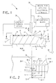
- Fig. 1 is a combined schematic and block diagram view of a system for testing a semiconductor wafer (shown in cross-section) having a topside and a beveled surface;
- Fig. 2 is a view taken along lines II-II in Fig. 1;
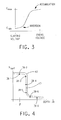
- Fig. 3 is an exemplary plot of changing capacitance versus changing voltage in response to the application of a CV-type electrical stimulus between a contact and a semiconductor wafer when the contact is pressing against the topside or the beveled surface of the semiconductor wafer;
- Fig. 4 are plots of electrically active dopant density (N SURF ) versus depth for the semiconductor wafer shown in Fig. 1 and a reference semiconductor wafer.
- a semiconductor wafer or sample test system 2 includes an electrically conductive vacuum chuck 4 and a contact 6.
- the illustration of contact 6 in the form of an elongated probe, however, is not to be construed as limiting the invention since it is envisioned that contact 6 can have any shape or form suitable for testing a semiconductor wafer or sample 10 under test.
- Chuck 4 is configured to support a backside 8 of semiconductor wafer or sample 10 under test, which includes a substrate 12 formed of a semiconducting material, which is held in contact with chuck 4 by means of a vacuum (not shown).
- substrate 12 of semiconductor wafer or sample 10 can be formed of any suitable semiconducting material known in the art, such as, without limitation, silicon (Si), geranium (Ge), gallium arsenide (GaAs), and the like.
- semiconductor wafer or sample 10 includes a dielectric or oxide layer 14 overlaying a topside of substrate 12.
- contact 6 has at least a partially spherical and conductive surface 20 for contacting a topside 16 of substrate 12, a topside 22 of dielectric layer 14, when present, or a beveled surface 24 (shown in Fig. 2) of substrate 12. While a partially spherical conductive surface 20 is desired, it is envisioned that surfaces (not shown) having other shapes suitable for testing a semiconductor wafer or sample 10 can be utilized. Accordingly, the illustration in Fig. 1 of conductive surface 20 being partially spherical is not to be construed as limiting the invention.
- a contact forming means 26 controls the vertical movement of chuck 4 and/or contact 6, in one or both of the directions shown by arrow 28, to move contact 6 and semiconductor wafer or sample 10 into contact whereupon conductive surface 20 presses into contact with topside 16 of substrate 12, topside 22 of dielectric layer 14, when present, or beveled surface 24 of substrate 12. Also or alternatively, contact forming means 26 can control the horizontal movement of vacuum chuck 4, contact 6, or both in one or both of the directions shown by arrow 29 to enable positioning of conductive surface 20 at desired test locations 38 (shown in Fig. 2) on topside 16 of substrate 12, topside 22 of dielectric layer 14, when present, or beveled surface 24 of substrate 12.
- a means for applying electrical stimulus 30 can be electrically connected to apply a suitable electrical stimulus (e.g., a CV-type electrical stimulus) to contact 6, semiconductor wafer or sample 10, or both when semiconductor wafer or sample 10 is received on chuck 4 and conductive surface 20 of contact 6 is in contact with topside 16, topside 22, when present, or beveled surface 24.
- a suitable electrical stimulus e.g., a CV-type electrical stimulus
- a measurement means 32 can be electrically connected for measuring the response of semiconductor wafer or sample 10 to the test stimulus applied by the means for applying electrical stimulus 30 and for processing the measured response in any suitable and/or desirable manner.
- a display 33, or any other suitable output means, can also be provided to enable measurement means 32 to output in a human perceivable form the results of any processing performed by measurement means 32 on the measured response of semiconductor wafer or sample 10.
- chuck 4 is connected to a reference ground 34.
- reference ground 34 is not to be construed as limiting the invention since chuck 4 alternatively can be connected to an AC or DC reference bias (not shown).
- a desired portion of semiconductor wafer or sample 10 is subject to lapping or grinding at a known small angle 50.
- the lapping or grinding of semiconductor wafer or sample 10 can be accomplished before or after semiconductor wafer or sample 10 is mounted on chuck 4.
- the lapping or grinding of semiconductor wafer or sample 10 removes a portion of dielectric layer 14 and a wedge shaped portion of substrate 12 adjacent topside 16 thereby forming beveled surface 24 of substrate 12.
- one or both of beveled surface 24 of substrate 12 and/or conductive surface 20 of contact 6 is a smooth, polished surface that maximizes contact between conductive surface 20 and beveled surface 24 when conductive surface 20 is pressed into contact with beveled surface 24.
- a plurality of CV-type measurements are made at a plurality of points laterally, desirably perpendicular, to a bevel edge 36 formed by the intersection of beveled surface 24 and topside 22 of dielectric layer 14.
- Each CV-type measurement is made by moving or pressing conductive surface 20 of contact 6 into contact with topside 22 of dielectric layer 14 or beveled surface 24 of substrate 12, whereupon a temporary capacitor is formed by the relationship of surface 20 in contact with topside 22 or beveled surface 24, and then applying a CV-type electrical stimulus to contact 6, semiconductor wafer or sample 10, or both.
- Fig. 2 shows a plurality of locations 38-1, 38-2, . .
- Each location 38 represents the contact area (A c ) between conductive surface 20 and topside 22 or beveled surface 24 when conductive surface 20 is in contact therewith.
- An exemplary CV-type electrical stimulus includes sweeping a DC voltage, having an AC voltage superimposed thereon, from a first, starting voltage where substrate 12 underlying conductive surface 20 is, desirably, in inversion and a minimum capacitance (C MIN ) is measured, to a second, ending voltage where substrate 12 underlying conductive surface 20 is, desirably, in accumulation and a maximum capacitance (C MAX ) is measured.
- FIG. 3 An exemplary CV plot illustrating the sweep of the DC voltage between a first, starting voltage and a second, ending voltage and the corresponding change in capacitance from C MIN to C MAX is shown in Fig. 3.
- a CV-type electrical stimulus where the DC voltage is swept from a first, starting voltage to a second, ending voltage is more desirable since it can be detected when semiconductor substrate 12 underlying conductive surface 20 enters accumulation whereupon an optimal value for C MAX can be acquired.
- the near surface electrically active dopant density (N SURF ) of semiconductor wafer 10 can be determined for said location 38 utilizing the corresponding acquired values of C MIN and C MAX and the following equation EQ 1 which is solved iteratively to determine the corresponding value for N SURF .
- C S q 2 ⁇ K s ⁇ ⁇ 0 ⁇ N SURF 2 ⁇ k ⁇ T 2 U F - 1 + ln ⁇ 1.15 ⁇
- C S A c ⁇ 1 C MIN - 1 C MAX - 1 ;
- a plot 40 (shown in dashed line) of N SURF versus depth can be formed from the value of N SURF determined at each test location 38. Plot 40 can then be compared to a reference plot 42 of N SURF versus depth determined theoretically or empirically utilizing a reference semiconductor wafer (not shown). Based on the degree of correlation between plot 40 and reference plot 42, it can be determined whether the near surface dopant density of the semiconductor wafer or sample 10 under test, and hence the efficacy of the ion doping of substrate 12, is within acceptable tolerance.
- the depth of each test location is a depth from the original location of topside 22 of dielectric layer 14.
- the depth of the test location 38 is the trigonometric sine of angle 50 multiplied by a distance 52 (measured parallel to topside 22 of dielectric layer 14) between bevel edge 36 and the center of the contact between conductive surface 20 and beveled surface 24.
- the depth of test location 38-3 is a distance 52-3 multiplied by the trigonometric sine of angle 50
- the depth of test location 38-4 is a distance 52-4 multiplied by the trigonometric sine of angle 50; and so forth.
- test locations 38-1 and 38-2 are on topside 22 of dielectric layer 14. Therefore, in plot 40 shown in Fig. 4, test locations 38-1 and 38-2 are shown at the same depth.
Landscapes
- Testing Or Measuring Of Semiconductors Or The Like (AREA)
Applications Claiming Priority (2)
| Application Number | Priority Date | Filing Date | Title |
|---|---|---|---|
| US79356506P | 2006-04-20 | 2006-04-20 | |
| US11/732,048 US20070249073A1 (en) | 2006-04-20 | 2007-04-02 | Method for determining the electrically active dopant density profile in ultra-shallow junction (USJ) structures |
Publications (2)
| Publication Number | Publication Date |
|---|---|
| EP1863078A2 true EP1863078A2 (fr) | 2007-12-05 |
| EP1863078A3 EP1863078A3 (fr) | 2009-04-15 |
Family
ID=38611006
Family Applications (1)
| Application Number | Title | Priority Date | Filing Date |
|---|---|---|---|
| EP07106417A Withdrawn EP1863078A3 (fr) | 2006-04-20 | 2007-04-18 | Procédé pour déterminer le profil de densité du dopant électriquement actif dans des structures à jonction ultra mince (USJ) |
Country Status (4)
| Country | Link |
|---|---|
| US (1) | US20070249073A1 (fr) |
| EP (1) | EP1863078A3 (fr) |
| JP (1) | JP2007294980A (fr) |
| TW (1) | TW200804834A (fr) |
Families Citing this family (3)
| Publication number | Priority date | Publication date | Assignee | Title |
|---|---|---|---|---|
| FR2941816B1 (fr) * | 2009-02-05 | 2011-04-01 | Commissariat Energie Atomique | Methode de caracterisation d'un procede d'implantation ionique. |
| CN111413634A (zh) * | 2020-03-27 | 2020-07-14 | 惠州亿纬集能有限公司 | 软包锂电池绝缘测试方法 |
| US11841296B2 (en) * | 2021-12-02 | 2023-12-12 | Globalfoundries U.S. Inc. | Semiconductor substrates for electrical resistivity measurements |
Family Cites Families (6)
| Publication number | Priority date | Publication date | Assignee | Title |
|---|---|---|---|---|
| US5521525A (en) * | 1994-04-15 | 1996-05-28 | University Of North Carolina | Method and apparatus for measuring the doping density profile of a semiconductor layer |
| DE19758348A1 (de) * | 1997-12-22 | 1999-06-24 | Inst Halbleiterphysik Gmbh | Verfahren zur Aufnahme von Tiefenprofilen zum Nachweis von Verunreinigungen in Halbleitern |
| US6492827B1 (en) * | 1999-10-19 | 2002-12-10 | Solid State Measurements, Inc. | Non-invasive electrical measurement of semiconductor wafers |
| US6741093B2 (en) * | 2000-10-19 | 2004-05-25 | Solid State Measurements, Inc. | Method of determining one or more properties of a semiconductor wafer |
| US6632691B1 (en) * | 2002-04-11 | 2003-10-14 | Solid State Measurements, Inc. | Apparatus and method for determining doping concentration of a semiconductor wafer |
| JP2005223098A (ja) * | 2004-02-04 | 2005-08-18 | Shin Etsu Handotai Co Ltd | ドーパント汚染の評価方法及び熱処理工程の管理方法並びにドーパント汚染量の測定方法 |
-
2007
- 2007-04-02 US US11/732,048 patent/US20070249073A1/en not_active Abandoned
- 2007-04-14 TW TW096113255A patent/TW200804834A/zh unknown
- 2007-04-18 EP EP07106417A patent/EP1863078A3/fr not_active Withdrawn
- 2007-04-20 JP JP2007135994A patent/JP2007294980A/ja active Pending
Also Published As
| Publication number | Publication date |
|---|---|
| EP1863078A3 (fr) | 2009-04-15 |
| US20070249073A1 (en) | 2007-10-25 |
| TW200804834A (en) | 2008-01-16 |
| JP2007294980A (ja) | 2007-11-08 |
Similar Documents
| Publication | Publication Date | Title |
|---|---|---|
| US5520769A (en) | Method for measuring concentration of dopant within a semiconductor substrate | |
| Schroder | Semiconductor material and device characterization | |
| US6395437B1 (en) | Junction profiling using a scanning voltage micrograph | |
| De Wolf et al. | One‐and two‐dimensional carrier profiling in semiconductors by nanospreading resistance profiling | |
| US6201401B1 (en) | Method for measuring the electrical potential in a semiconductor element | |
| JPH04225247A (ja) | 材料物性測定方法及び装置 | |
| US6265890B1 (en) | In-line non-contact depletion capacitance measurement method and apparatus | |
| Huang et al. | Direct comparison of cross‐sectional scanning capacitance microscope dopant profile and vertical secondary ion‐mass spectroscopy profile | |
| Huang et al. | Quantitative two‐dimensional dopant profiling of abrupt dopant profiles by cross‐sectional scanning capacitance microscopy | |
| Kopanski et al. | Scanning capacitance microscopy measurement of two-dimensional dopant profiles across junctions | |
| US6741093B2 (en) | Method of determining one or more properties of a semiconductor wafer | |
| US8004290B1 (en) | Method and apparatus for determining dielectric layer properties | |
| EP1863078A2 (fr) | Procédé pour déterminer le profil de densité du dopant électriquement actif dans des structures à jonction ultra mince (USJ) | |
| Nxumalo et al. | Cross‐sectional imaging of semiconductor device structures by scanning resistance microscopy | |
| Eyben et al. | Probing semiconductor technology and devices with scanning spreading resistance microscopy | |
| Henning et al. | Scanning probe microscopy for 2-D semiconductor dopant profiling and device failure analysis | |
| JPH10270515A (ja) | 電気特性測定装置 | |
| Stangoni | Scanning probe techniques for dopant profile characterization | |
| US6287880B1 (en) | Method and apparatus for high resolution profiling in semiconductor structures | |
| US20080290889A1 (en) | Method of destructive testing the dielectric layer of a semiconductor wafer or sample | |
| US7521946B1 (en) | Electrical measurements on semiconductors using corona and microwave techniques | |
| Tran et al. | Quantitative two-dimensional carrier profiling of a 400 nm complementary metal–oxide–semiconductor device by Schottky scanning capacitance microscopy | |
| US7037734B2 (en) | Method and apparatus for determining generation lifetime of product semiconductor wafers | |
| US7250313B2 (en) | Method of detecting un-annealed ion implants | |
| US6320403B1 (en) | Method of determining the doping concentration and defect profile across a surface of a processed semiconductor material |
Legal Events
| Date | Code | Title | Description |
|---|---|---|---|
| PUAI | Public reference made under article 153(3) epc to a published international application that has entered the european phase |
Free format text: ORIGINAL CODE: 0009012 |
|
| AK | Designated contracting states |
Kind code of ref document: A2 Designated state(s): AT BE BG CH CY CZ DE DK EE ES FI FR GB GR HU IE IS IT LI LT LU LV MC MT NL PL PT RO SE SI SK TR |
|
| AX | Request for extension of the european patent |
Extension state: AL BA HR MK YU |
|
| PUAL | Search report despatched |
Free format text: ORIGINAL CODE: 0009013 |
|
| AK | Designated contracting states |
Kind code of ref document: A3 Designated state(s): AT BE BG CH CY CZ DE DK EE ES FI FR GB GR HU IE IS IT LI LT LU LV MC MT NL PL PT RO SE SI SK TR |
|
| AX | Request for extension of the european patent |
Extension state: AL BA HR MK RS |
|
| AKX | Designation fees paid | ||
| REG | Reference to a national code |
Ref country code: DE Ref legal event code: 8566 |
|
| STAA | Information on the status of an ep patent application or granted ep patent |
Free format text: STATUS: THE APPLICATION IS DEEMED TO BE WITHDRAWN |
|
| 18D | Application deemed to be withdrawn |
Effective date: 20091013 |