EP1865329A1 - Capteur d'acceleration a semi-conducteurs - Google Patents
Capteur d'acceleration a semi-conducteurs Download PDFInfo
- Publication number
- EP1865329A1 EP1865329A1 EP06730429A EP06730429A EP1865329A1 EP 1865329 A1 EP1865329 A1 EP 1865329A1 EP 06730429 A EP06730429 A EP 06730429A EP 06730429 A EP06730429 A EP 06730429A EP 1865329 A1 EP1865329 A1 EP 1865329A1
- Authority
- EP
- European Patent Office
- Prior art keywords
- diaphragm
- axis
- center
- acceleration sensor
- semiconductor acceleration
- Prior art date
- Legal status (The legal status is an assumption and is not a legal conclusion. Google has not performed a legal analysis and makes no representation as to the accuracy of the status listed.)
- Granted
Links
Images




Classifications
-
- G—PHYSICS
- G01—MEASURING; TESTING
- G01P—MEASURING LINEAR OR ANGULAR SPEED, ACCELERATION, DECELERATION, OR SHOCK; INDICATING PRESENCE, ABSENCE, OR DIRECTION, OF MOVEMENT
- G01P15/00—Measuring acceleration; Measuring deceleration; Measuring shock, i.e. sudden change of acceleration
- G01P15/02—Measuring acceleration; Measuring deceleration; Measuring shock, i.e. sudden change of acceleration by making use of inertia forces using solid seismic masses
- G01P15/08—Measuring acceleration; Measuring deceleration; Measuring shock, i.e. sudden change of acceleration by making use of inertia forces using solid seismic masses with conversion into electric or magnetic values
- G01P15/12—Measuring acceleration; Measuring deceleration; Measuring shock, i.e. sudden change of acceleration by making use of inertia forces using solid seismic masses with conversion into electric or magnetic values by alteration of electrical resistance
- G01P15/123—Measuring acceleration; Measuring deceleration; Measuring shock, i.e. sudden change of acceleration by making use of inertia forces using solid seismic masses with conversion into electric or magnetic values by alteration of electrical resistance by piezo-resistive elements, e.g. semiconductor strain gauges
-
- G—PHYSICS
- G01—MEASURING; TESTING
- G01P—MEASURING LINEAR OR ANGULAR SPEED, ACCELERATION, DECELERATION, OR SHOCK; INDICATING PRESENCE, ABSENCE, OR DIRECTION, OF MOVEMENT
- G01P15/00—Measuring acceleration; Measuring deceleration; Measuring shock, i.e. sudden change of acceleration
- G01P15/18—Measuring acceleration; Measuring deceleration; Measuring shock, i.e. sudden change of acceleration in two or more dimensions
-
- G—PHYSICS
- G01—MEASURING; TESTING
- G01P—MEASURING LINEAR OR ANGULAR SPEED, ACCELERATION, DECELERATION, OR SHOCK; INDICATING PRESENCE, ABSENCE, OR DIRECTION, OF MOVEMENT
- G01P15/00—Measuring acceleration; Measuring deceleration; Measuring shock, i.e. sudden change of acceleration
- G01P15/02—Measuring acceleration; Measuring deceleration; Measuring shock, i.e. sudden change of acceleration by making use of inertia forces using solid seismic masses
- G01P15/08—Measuring acceleration; Measuring deceleration; Measuring shock, i.e. sudden change of acceleration by making use of inertia forces using solid seismic masses with conversion into electric or magnetic values
- G01P2015/0805—Measuring acceleration; Measuring deceleration; Measuring shock, i.e. sudden change of acceleration by making use of inertia forces using solid seismic masses with conversion into electric or magnetic values being provided with a particular type of spring-mass-system for defining the displacement of a seismic mass due to an external acceleration
- G01P2015/0822—Measuring acceleration; Measuring deceleration; Measuring shock, i.e. sudden change of acceleration by making use of inertia forces using solid seismic masses with conversion into electric or magnetic values being provided with a particular type of spring-mass-system for defining the displacement of a seismic mass due to an external acceleration for defining out-of-plane movement of the mass
- G01P2015/084—Measuring acceleration; Measuring deceleration; Measuring shock, i.e. sudden change of acceleration by making use of inertia forces using solid seismic masses with conversion into electric or magnetic values being provided with a particular type of spring-mass-system for defining the displacement of a seismic mass due to an external acceleration for defining out-of-plane movement of the mass the mass being suspended at more than one of its sides, e.g. membrane-type suspension, so as to permit multi-axis movement of the mass
Definitions
- the present invention relates to a semiconductor acceleration sensor, and more particularly to a semiconductor acceleration sensor that senses accelerations in directions orthogonal to each other with respective proper sensitivities.
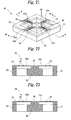
- Figure 21 is an external perspective view
- Figure 22 is a cross-sectional view observed from the arrow direction along the line A-A shown in Figure 21
- Figure 23 is a cross-sectional view observed from the arrowdirection along the line B-B shown in Figure 21.
- the semiconductor acceleration sensor 20 includes a pedestal 21 having a rectangular frame shape and is constituted of a silicon substrate 22 mounted on one opening plane of the pedestal 21.
- a diaphragm 23 of thin film having a cross shape on the upper surface of each of the diaphragmpieces 23a to 23d, there is formed a piezo resistor 26.
- a thick film section 24 On one surface side of the center of the diaphragm 23 in the crossing section of the diaphragm pieces 23a to 23d, there is formed a thick film section 24; on the surface of the thick film section 24, there is mounted a plumb bob 25 having a rectangular solid shape made of, for example, glass.
- an acceleration sensor when an acceleration sensor is arranged with the longitudinal direction of a vehicle corresponding to the X axis, the lateral direction to the Y axis and the vertical direction to the Z axis, a maximum acceleration of about 500 G is sensed in the X-axis direction and on the other hand, an acceleration of about several G at most is sensed in the Y-axis direction. Accordingly, a semiconductor acceleration sensor having a different sensitivity is required depending on the direction of acceleration.
- the acceleration sensitivity is approximately identical in the X axis, Y axis and Z axis directions.
- an object of the present invention is to provide a semiconductor acceleration sensor capable of sensing accelerations in two directions parallel to the surface of a diaphragm and orthogonal to each other with respective proper sensitivities.
- the present invention proposes a semiconductor acceleration sensor comprising: a silicon wafer having a diaphragm formed within a wafer outer-circumferential frame section; a pedestal securing the wafer outer-circumferential frame section; a plumb bob disposed in the center of one surface of the diaphragm; and a plurality of beams extending, respectively, from the center of surface of the diaphragm to the wafer outer-circumferential frame section along X axis and Y axis directions parallel to the surface of the diaphragm and orthogonal to each other, wherein the areas of cross section of the plurality of beams orthogonal to each axis at a predetermined position are set according to a maximum value of respective accelerations in the X axis and Y axis directions.
- the semiconductor acceleration sensor having the above described configuration, there are provided the plurality of beams extending, respectively, from the center of surface of the diaphragm to the wafer outer-circumferential frame section along the X axis and Y axis directions parallel to the surface of the diaphragm and orthogonal to each other, and the areas of cross section of the beams orthogonal to each axis at the predetermined position are set according to the maximum value of respective accelerations in the X axis and Y axis directions.
- the diaphragm is distorted in a direction of the force working, but the displacement is inversely proportional to the cross section area of the diaphragm. Accordingly, when accelerations having the same amplitude are exerted, respectively, in the X axis and Y axis directions, each of the beams are displaced in inverse proportion to the maximum value of acceleration in each axis.
- the present invention proposes the semiconductor acceleration sensor having the above described configuration, wherein in each of the beam disposed along the X axis direction and the beam disposed along the Y axis direction, the cross section area at two points symmetrical around the center is identical.
- the cross section area at two points symmetrical around the center is identical.
- the diaphragm is distorted in a direction of the force working, but the displacement is inversely proportional to the cross section area of the diaphragm. Accordingly, each of the beams are displaced symmetrically around the center.
- the present invention proposes the semiconductor acceleration sensor having the above described configuration, wherein in the beam disposed along the X axis direction and/or the beam disposed along the Y axis direction, the cross section area increases in a direction from the center to the wafer outer-circumferential frame section.
- the cross section area of at least one of the beam disposed along the X axis direction and the beam disposed along the Y axis direction increases in a direction from the center to the wafer outer-circumferential frame section.
- the diaphragm is distorted in a direction of the force working, but the displacement is inversely proportional to the cross section area of the diaphragm. Accordingly, the nearer the center, the larger the displacement of each of the beams.
- the present invention proposes the semiconductor acceleration sensor having the above described configuration, wherein to allow sensing of respective accelerations in the X axis and Y axis directions and a Z axis direction orthogonal to the surface of the diaphragm, a diffused resistor is arranged in each of the plurality of beams and at the same time, on the wafer outer-circumferential frame section corresponding to each of the plurality of beams, there is provided an connection electrode connected to the diffused resistor.
- the diffused resistor is arranged along each of the plurality of beams, and these diffused resistors are each connected to the electrode disposed on the wafer outer-circumferential frame section. Accordingly, an external circuit can be connected to the diffused resistor via the electrode, and the resistance value of the diffused resistor varies in association with displacement of the diaphragm.
- the present invention proposes the semiconductor acceleration sensor having the above described configuration, wherein the diaphragm is a silicon piezo diaphragm.
- the resistance value of the piezo resistor varies in association with displacement of the diaphragm.
- the present invention proposes the semiconductor acceleration sensor having the above described configuration, wherein in one surface side and/or the other surface side of the diaphragm, there is provided a protrusion secured to a position spaced with a predetermined gap from the surface of the center of the diaphragm and/or from the surface of the plumb bob corresponding to the center, and protruding opposite the center.
- the semiconductor acceleration sensor having the above described configuration, when force of a predetermined value or more is exerted by an acceleration generated in a direction orthogonal to the surface of the diaphragm, the diaphragm is distorted and stretched in a direction of the force working. However, the displacement is limited by the protrusion, so the diaphragm cannot be stretched to a maximum. Accordingly, when an excessive acceleration is generated in a direction orthogonal to the surface of the diaphragm, also, the position of the plumb bob changes with the tip end of the protrusion acting as a supporting point, so an acceleration in a direction parallel to the surface of the diaphragm can be sensed.
- the present invention proposes the semiconductor acceleration sensor having the above described configuration, wherein the protrusion is secured and supported to the wafer outer-circumferential frame section and/or the pedestal and disposed at a position spaced with a predetermined gap from the center of the other surface of the diaphragm so as to protrude opposite the center of the other surface of the diaphragm.
- the semiconductor acceleration sensor having the above described configuration, when force of a predetermined value or more is exerted on the other surface side of the diaphragm by an acceleration generated in a direction orthogonal to the surface of the diaphragm, the diaphragm is distorted and stretched in a direction of the force working. However, the displacement is limited by the protrusion, so the diaphragm cannot be stretched to a maximum. Accordingly, when force of the predetermined value or more is exerted on the other surface side of the diaphragm, also, the position of the plumb bob changes with the tip end of the protrusion acting as a supporting point, so an acceleration in a direction parallel to the surface of the diaphragm can be sensed.
- the present invention proposes the semiconductor acceleration sensor having the above described configuration, wherein the protrusion is joined and supported to the wa f er outer-circumferential frame section and/or the pedestal and disposed at a position spaced with a predetermined gap from the center of the plumb bob so as to protrude opposite the surface of the plumb bob.
- the semiconductor acceleration sensor having the above described configuration, when force of a predetermined value or more is exerted on one surface side of the diaphragm by an acceleration generated in a direction orthogonal to the surface of the diaphragm, the diaphragm is distorted and stretched in a direction of the force working. However, the displacement is limited by the protrusion, so the diaphragm cannot be stretched to a maximum. Accordingly, when force of the predetermined value or more is exerted on the one surface side of the diaphragm, also, the position of the plumb bob changes with the tip end of the protrusion acting as a supporting point, so an acceleration in a direction parallel to the surface of the diaphragm can be sensed.
- the present invention proposes the semiconductor acceleration sensor having the above described configuration, wherein the tip end of the protrusion corresponding to the surface of the center of the diaphragm and/or to the surface of the plumb bob corresponding to the center has a cone-shaped tip end configuration.
- the semiconductor acceleration sensor having the above described configuration, when force of a predetermined value or more is exerted by an acceleration generated in a direction orthogonal to the surface of the diaphragm, the diaphragm is distorted and stretched in a direction of the force working. However, the displacement is supported and limited by the cone-shaped tip end of the protrusion, so the diaphragm cannot be stretched to a maximum. At the same time, when an excessive acceleration is generated in a direction orthogonal to the surface of the diaphragm, also, the position of the plumb bob changes with the tip end of the protrusion acting as a supporting point, so an acceleration in a direction parallel to the surface of the diaphragm can be sensed.
- the area of cross section orthogonal to the X axis of the diaphragm pieces being the beams disposed on a single line along the X axis direction and the area of cross section orthogonal to the Y axis of the diaphragm pieces being the beams disposed on a single line along the Y axis direction are each symmetrical around the central of the diaphragm and set according to a maximum value of respective accelerations in the X axis or Y axis directions, the X axis and Y axis being parallel to the surface of the diaphragm and orthogonal to each other.
- FIG 1 is an external perspective view showing a semiconductor acceleration sensor according to a first embodiment of the present invention.
- the semiconductor acceleration sensor 10 is constituted of a pedestal 11 and a silicon substrate 12.
- the pedestal 11 has a rectangular frame shape.
- the silicon substrate 12 silicon wafer
- the silicon substrate 12 In the opening of the pedestal 11, there is provided the silicon substrate 12; in the center within a wafer outer-circumferential frame section 12a of the silicon substrate 12, there is formed a diaphragm 13 of thin film having a cross shape.
- the diaphragm 13 is constituted of diaphragm pieces 13a to 13d being four beams each extending from the center of the diaphragm surface to the wafer outer-circumferential frame section 12a along an X axis direction and a Y axis direction orthogonal to each other; on the upper surface of the diaphragm pieces, there are formed piezo resistors (diffused resistors) Rx1 to Rx4, Ry1 to Ry4, Rz1 to Rz4.
- one diaphragm piece 13a of the diaphragm pieces 13a and 13b disposed on a single line there are formed the piezo resistors Rx1, Rx2, Rz1 and Rz2; in the other diaphragm piece 13b, there are formed the piezo resistors Rx3, Rx4, Rz3 and Rz4.
- the piezo resistors Ry1 and Ry2 in the other diaphragm piece 13d, there are formed the piezo resistors Ry3 and Ry4.
- the piezo resistors Rx1 to Rx4, Ry1 to Ry4, and Rz1 to Rz4 are connected to a connection electrode 121 disposed on the surface of the outer-circumferential section of the silicon substrate 12 so that they can constitute a resistor bridge circuit for sensing accelerations in the directions of the X axis, Y axis and Z axis orthogonal to each other.
- a thick film section 14 On one surface side of the center of the diaphragm 13 in the crossing section of the diaphragm pieces 13a to 13d, there is formed a thick film section 14; on the surface of the thick film section 14, there is mounted a plumb bob 15 having a rectangular solid shape made of, for example, glass.
- FIG. 3 When the semiconductor acceleration sensor 10 having the above described configuration is used, three resistor bridge circuits are constructed as shown in Figures 3 to 5. More specifically, in a bridge circuit for sensing an acceleration in the X axis direction, as shown in Figure 3, the positive electrode of a DC power supply 32A is connected to a connection point between one end of a piezo resistor Rx1 and one end of a piezo resistor Rx2, and the negative electrode of the direct current power source 32A is connected to a connection point between one end of a piezo resistor Rx3 and one end of a piezo resistor Rx4.
- one end of a voltage detector 31A is connected to a connection point between the other end of the piezo resistor Rx1 and the other end of the piezo resistor Rx4, and the other end of the voltage detector 31A is connected to a connection point between the other end of the piezo resistor Rx2 and the other end of the piezo resistor Rx3.
- the positive electrode of a DC power supply 32B is connected to a connection point between one end of a piezo resistor Ry1 and one end of a piezo resistor Ry2, and the negative electrode of the DC power supply 32B is connected to a connection point between one end of a piezo resistor Ry3 and one end of a piezo resistor Ry4.
- one end of a voltage detector 31B is connected to a connection point between the other end of the piezo resistor Ry1 and the other end of the piezo resistor Ry4, and the other end of the voltage detector 31B is connected to a connection point between the other end of the piezo resistor Ry2 and the other end of the piezo resistor Ry3.
- the positive electrode of a DC power supply 32C is connected to a connection point between one end of a piezo resistor Rz1 and one end of a piezo resistor Rz2, and the negative electrode of the DC power supply 32C is connected to a connection point between one end of a piezo resistor Rz3 and one end of a piezo resistor Rz4.
- one end of a voltage detector 31C is connected to a connection point between the other end of the piezo resistor Rz1 and the other end of the piezo resistor Rz3, and the other end of the voltage detector 31C is connected to a connection point between the other end of the piezo resistor Rz2 and the other end of the piezo resistor Rz4.
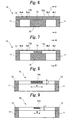
- Figure 6 is a cross-sectional view observed from the arrow direction along the lineC-C shown in Figure 1;
- Figure 7 is a cross-sectionalviewobserved from the arrow direction along the line D-D shown in Figure 1;
- Figure 8 is a cross-sectional view observed from the arrow direction along the line C1-C1 shown in Figure 6;
- Figure 9 is a cross-sectional view observed from the arrow direction along the line D1-D1 shown in Figure 7.
- the areas of cross section orthogonal to each axis are uniform and set according to a maximum value of acceleration, respectively, in the X axis direction or the Y axis direction.
- accelerations are sensed with the longitudinal direction of a vehicle corresponding to the X axis and the lateral direction to the Y axis, and the cross section area of the diaphragm pieces 13a and 13b along the X axis direction is set larger than that of the diaphragm pieces 13c and 13d along the Y axis direction.
- the diaphragm 13 When force by acceleration is exerted, the diaphragm 13 distorts in a direction of the force working. However, its displacement is in inverse proportion to the cross section area of the diaphragm pieces 13a to 13d. Consequently, when an acceleration of the same amplitude is applied in each of the X axis direction and Y axis direction, the diaphragm pieces 13a to 13d are displaced in inverse proportion to the maximum value of acceleration in each axis. Also, the cross section areas of each of the diaphragm pieces 13a to 13d are uniform and symmetrical around the center of the diaphragm 13, so the diaphragm pieces are displaced symmetrically around the center.
- each said diaphragm pieces 13a to 13d are 70 [ ⁇ m] and 20 [ ⁇ m], respectively.
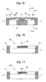
- experimental results of accelerations sensed by the diaphragm 13 is shown in Figure 11.
- the applied acceleration is 0 to 100 [G]
- the difference between the sensed accelerations in the directions of the X axis and Y axis and the applied acceleration was 1 % or less
- the difference between the sensed acceleration in the Z axis direction and the applied acceleration was 3 % or less.
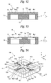
- the diaphragm 13 in which the cross section areas of each said diaphragm pieces 13a to 13d are uniform. However, it is sufficient that the cross section areas of each said diaphragm pieces 13a to 13d are symmetrical around the center of the diaphragm 13. As shown in Figures 14 to 17, in the diaphragm pieces 13a and 13b disposed on a single line along the X axis direction, when the cross section area increases in a direction from the center of the diaphragm 13 to the wafer outer-circumferential frame section 12a, then the nearer the center of the diaphragm, the larger the displacement of the diaphragm pieces 13a and 13b. Particularly, the cross section area is varied stepwise between the position of the piezo resistors Rx1 to Rx4 formed and the other position, so the variation in resistance value of the piezo resistors Rx1 to Rx4 is significant.
- the semiconductor acceleration sensor 10 having the above described configuration, with respect to the diaphragm pieces 13a and 13b disposed on a single line along the X axis direction and the diaphragm pieces 13c and 13d disposed on a single line along the Y axis direction, the X axis and Y axis being parallel to the surface of the diaphragm and orthogonal to each other, the areas of cross section orthogonal to each axis are symmetrical around the central of the diaphragm 13 and set according to a maximum value of respective accelerations in the X axis or Y axis direction.
- the cross section areas increase in a direction from the center of the diaphragm 13 to the wafer outer-circumferential frame section 12a, so the nearer the center of the diaphragm 13, the larger the displacement of the diaphragm pieces 13a to 13d and at the same time, the more significant the variation in the piezo resistors Rx1 to Rx4, Ry1 to Ry4, Rz1 to Rz4, thus allowing sensing of accelerations with higher accuracy.
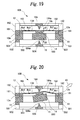
- Figure 18 is an exploded perspective view showing a semiconductor acceleration sensor according to a second embodiment of the present invention
- Figure 19 is a side cross sectional view thereof
- Figure 20 is a view for explaining the operation thereof.
- the same reference characters denote constituent parts corresponding to the first embodiment described above, and an explanation thereof is omitted.
- the difference between the second embodiment and the first embodiment lies in that the second embodiment includes in addition to the configuration of the first embodiment, support bodies 16 and 50 having protrusions disposed both in one side where the plumb bob 15 of the diaphragm 13 is present and the other side where the plumb bob 15 of the diaphragm 13 is not present.
- the semiconductor acceleration sensor 10B is constituted of a pedestal 11, a silicon substrate 12 and the support bodies 16 and 50. To the outer-circumferential section of the pedestal 11, there is secured an outer frame section 161 of the support body 16.
- the support body 16 is constituted of the outer frame section 161 having a rectangular frame shape, four supporting columns 162 installed in the four corners of the outer frame section 161, a beam section 163 having a cross shape disposed so as to join the tip ends of each supporting column 162, and a protrusion 164 having a cone shape disposed in the central, crossing part of the beam section 163.
- the outer frame section 161 is fit into the outer-circumferential section of the pedestal 11 to be secured, so that the protrusion 164 is positioned in the other surface side of the diaphragm 13, i.e., in the side where the plumb bob 15 is not present.
- a setting is made such that the tip end 164a of the protrusion 164 is positioned at a distance d1 from the surface of the diaphragm 13.
- the distance d1 is set to a value by which the displacement of each of the diaphragm pieces 13c and 13d can be limited by the protrusion 164 so that the diaphragm pieces are not stretched excessively even when an acceleration is generated in a direction orthogonal to the surface of the diaphragm 13 and force of a predetermined value or more caused by the acceleration is exerted on the other surface side of the diaphragm 13, i.e., on the side where the plumb bob 15 is not present.
- the support body 50 is constituted of an outer frame section 501 having a rectangular frame shape, four supporting columns 502 installed in the four corners of the outer frame section 501, a beam section 503 having a cross shape disposed so as to join the tip ends of each supporting column 502, and a protrusion 504 having a cone shape disposed in the central, crossing part of the beam section 503.
- the outer frame section 501 is secured to the outer-circumferential section of the pedestal 11 so that the protrusion 504 is positioned in the bottom surface side of the plumb bob 15.
- a setting is made such that the tip end 504a of the protrusion 504 is positioned at a distance dl from the bottom surface side of the plumb bob 15.
- the distance dl is set to a value by which the displacement of each of the diaphragm pieces 13c and 13d can be limited by the protrusion 504 so that the diaphragm pieces are not stretched excessively even when an acceleration is generated in a direction orthogonal to the surface of the diaphragm 13 and force of a predetermined value or more caused by the acceleration is exerted on one surface side of the diaphragm 13, i.e., on the side where the plumb bob 15 is present.
- an acceleration sensor with a plurality of beams whose cross section area orthogonal, respectively, to one of the X axis and Y axis directions parallel to the surface of the diaphragm and orthogonal to each other are set according to a maximum value of acceleration in the X axis or Y axis direction, accelerations in the X axis and Y axis directions can be sensed with respective proper sensitivities. Accordingly, the sensor is applicable to a vehicle for which different sensitivity between the longitudinal direction and lateral direction of the vehicle is required.
Landscapes
- Physics & Mathematics (AREA)
- General Physics & Mathematics (AREA)
- Pressure Sensors (AREA)
Applications Claiming Priority (2)
| Application Number | Priority Date | Filing Date | Title |
|---|---|---|---|
| JP2005097901A JP2006275896A (ja) | 2005-03-30 | 2005-03-30 | 半導体加速度センサ |
| PCT/JP2006/306481 WO2006106739A1 (fr) | 2005-03-30 | 2006-03-29 | Capteur d'acceleration a semi-conducteurs |
Publications (3)
| Publication Number | Publication Date |
|---|---|
| EP1865329A1 true EP1865329A1 (fr) | 2007-12-12 |
| EP1865329A4 EP1865329A4 (fr) | 2010-02-10 |
| EP1865329B1 EP1865329B1 (fr) | 2012-03-07 |
Family
ID=37073302
Family Applications (1)
| Application Number | Title | Priority Date | Filing Date |
|---|---|---|---|
| EP06730429A Ceased EP1865329B1 (fr) | 2005-03-30 | 2006-03-29 | Capteur d'acceleration a semi-conducteurs |
Country Status (4)
| Country | Link |
|---|---|
| US (1) | US7827865B2 (fr) |
| EP (1) | EP1865329B1 (fr) |
| JP (1) | JP2006275896A (fr) |
| WO (1) | WO2006106739A1 (fr) |
Families Citing this family (9)
| Publication number | Priority date | Publication date | Assignee | Title |
|---|---|---|---|---|
| KR100895037B1 (ko) | 2007-02-05 | 2009-05-04 | (주)에스엠엘전자 | 고감도 3축 가속도 센서 |
| US8733176B2 (en) * | 2009-09-02 | 2014-05-27 | Kontel Data System Limited | MEMS stress concentrating structure for MEMS sensors |
| KR101119283B1 (ko) * | 2009-12-22 | 2012-06-05 | 삼성전기주식회사 | 관성 센서 및 그 제조 방법 |
| DE102010002994A1 (de) * | 2010-03-18 | 2011-09-22 | Robert Bosch Gmbh | Piezoresistives mikromechanisches Sensorbauelement und entsprechendes Messverfahren |
| WO2011157882A2 (fr) * | 2010-06-18 | 2011-12-22 | Baolab Microsystems Sl | Accéléromètre à ressort électrostatique instable |
| TWI477780B (zh) * | 2011-10-12 | 2015-03-21 | Richwave Technology Corp | 壓阻式z軸加速度感測器 |
| JP6294463B2 (ja) * | 2014-03-20 | 2018-03-14 | 京セラ株式会社 | センサ |
| JP6420442B1 (ja) * | 2017-10-16 | 2018-11-07 | 株式会社ワコー | 発電素子 |
| CN113933538B (zh) * | 2021-09-18 | 2024-07-19 | 重庆邮电大学 | 一种压阻式高g值加速度计 |
Family Cites Families (22)
| Publication number | Priority date | Publication date | Assignee | Title |
|---|---|---|---|---|
| WO1988008522A1 (fr) * | 1987-04-24 | 1988-11-03 | Kabushiki Kaisha Nexy Kenkyusho | Detecteur de forces, d'acceleration et de magnetisme, utilisant des resistances |
| US5081867A (en) * | 1988-09-30 | 1992-01-21 | Nec Corporation | Semiconductor sensor |
| US5209117A (en) * | 1990-10-22 | 1993-05-11 | Motorola, Inc. | Tapered cantilever beam for sensors |
| US5412986A (en) * | 1990-12-21 | 1995-05-09 | Texas Instruments Incorporated | Accelerometer with improved strain gauge sensing means |
| US5351542A (en) * | 1992-01-27 | 1994-10-04 | Kansei Corporation | Acceleration sensor assembly |
| JP3391841B2 (ja) * | 1993-05-26 | 2003-03-31 | 松下電工株式会社 | 半導体加速度センサ |
| JPH0875775A (ja) | 1994-09-08 | 1996-03-22 | Fujikura Ltd | 半導体型加速度センサ |
| JPH09119943A (ja) | 1995-10-24 | 1997-05-06 | Wako:Kk | 加速度センサ |
| JPH09292409A (ja) | 1996-04-26 | 1997-11-11 | Hitachi Ltd | 加速度センサ |
| CA2251957C (fr) * | 1997-02-21 | 2003-07-01 | Matsushita Electric Works, Ltd. | Element detecteur d'acceleration et son procede de production |
| JP2000028633A (ja) | 1998-07-08 | 2000-01-28 | Japan Aviation Electronics Ind Ltd | 半導体加速度センサ |
| JP2003172745A (ja) * | 2001-09-26 | 2003-06-20 | Hitachi Metals Ltd | 半導体加速度センサ |
| JP4216525B2 (ja) * | 2002-05-13 | 2009-01-28 | 株式会社ワコー | 加速度センサおよびその製造方法 |
| JP2004198280A (ja) * | 2002-12-19 | 2004-07-15 | Hitachi Metals Ltd | 加速度センサ |
| JP2004340616A (ja) | 2003-05-13 | 2004-12-02 | Yokohama Rubber Co Ltd:The | 半導体加速度センサ |
| JP4137710B2 (ja) | 2003-06-11 | 2008-08-20 | シャープ株式会社 | パネルセンサおよびこれを備えた情報機器 |
| JP4179070B2 (ja) | 2003-06-25 | 2008-11-12 | 松下電工株式会社 | 半導体加速度センサおよびその製造方法 |
| EP1491901A1 (fr) * | 2003-06-25 | 2004-12-29 | Matsushita Electric Works, Ltd. | Capteur d'accélération sémiconducteur et méthode pour sa fabrication |
| JP4416460B2 (ja) * | 2003-09-16 | 2010-02-17 | トレックス・セミコンダクター株式会社 | 加速度センサー |
| WO2005062060A1 (fr) * | 2003-12-24 | 2005-07-07 | Hitachi Metals, Ltd. | Capteur d'acceleration a 3 axes de type a semi-conducteur |
| US7367232B2 (en) * | 2004-01-24 | 2008-05-06 | Vladimir Vaganov | System and method for a three-axis MEMS accelerometer |
| TWI277735B (en) * | 2004-09-30 | 2007-04-01 | Hitachi Metals Ltd | Semiconductor acceleration sensor |
-
2005
- 2005-03-30 JP JP2005097901A patent/JP2006275896A/ja active Pending
-
2006
- 2006-03-29 US US11/815,556 patent/US7827865B2/en not_active Expired - Fee Related
- 2006-03-29 EP EP06730429A patent/EP1865329B1/fr not_active Ceased
- 2006-03-29 WO PCT/JP2006/306481 patent/WO2006106739A1/fr not_active Ceased
Also Published As
| Publication number | Publication date |
|---|---|
| JP2006275896A (ja) | 2006-10-12 |
| EP1865329A4 (fr) | 2010-02-10 |
| US20080271535A1 (en) | 2008-11-06 |
| EP1865329B1 (fr) | 2012-03-07 |
| US7827865B2 (en) | 2010-11-09 |
| WO2006106739A1 (fr) | 2006-10-12 |
Similar Documents
| Publication | Publication Date | Title |
|---|---|---|
| JP5965934B2 (ja) | 改善されたオフセットおよびノイズ性能を有する傾斜モード加速度計 | |
| EP2899502B1 (fr) | Capteur de force d'inertie | |
| JP2776142B2 (ja) | 加速度センサ | |
| EP2056068B1 (fr) | Capteur de force d'inertie | |
| JP2008145440A (ja) | 変動する表面負荷に対する感度が低下されたマイクロマシン構造の慣性センサ、及び慣性センサを駆動するために適した方法 | |
| US20110174076A1 (en) | Multiaxial micromechanical acceleration sensor | |
| JPS62174978A (ja) | 半導体振動・加速度検出装置 | |
| EP1865329A1 (fr) | Capteur d'acceleration a semi-conducteurs | |
| US11255873B2 (en) | Increased sensitivity z-axis accelerometer | |
| US8074517B2 (en) | Inertia force sensor | |
| JP3147786B2 (ja) | 加速度センサ | |
| JP2003248016A (ja) | 容量式加速度センサ | |
| JPH11242052A (ja) | 半導体加速度センサ | |
| JP2004340616A (ja) | 半導体加速度センサ | |
| US6474134B1 (en) | Method for adjusting sensitivity of acceleration sensor | |
| JP4525452B2 (ja) | 多軸加速度センサ | |
| KR101454124B1 (ko) | 가속도 센서 | |
| JP2010164569A (ja) | 多軸加速度センサ | |
| JPH07140167A (ja) | 容量型加速度センサ | |
| JP2003136494A (ja) | マイクロ構造体、物理量検出装置及びその製造方法 | |
| JPH08160070A (ja) | 加速度センサ | |
| JPH11248741A (ja) | 静電容量型多軸加速度センサ | |
| JP2999291B2 (ja) | 多次元方向に関する力・加速度・磁気の検出装置 | |
| JPH075193A (ja) | 多軸加速度検出装置 | |
| JPH08160067A (ja) | 加速度センサ |
Legal Events
| Date | Code | Title | Description |
|---|---|---|---|
| PUAI | Public reference made under article 153(3) epc to a published international application that has entered the european phase |
Free format text: ORIGINAL CODE: 0009012 |
|
| 17P | Request for examination filed |
Effective date: 20070330 |
|
| AK | Designated contracting states |
Kind code of ref document: A1 Designated state(s): DE FR |
|
| DAX | Request for extension of the european patent (deleted) | ||
| RBV | Designated contracting states (corrected) |
Designated state(s): DE FR |
|
| A4 | Supplementary search report drawn up and despatched |
Effective date: 20100112 |
|
| 17Q | First examination report despatched |
Effective date: 20100324 |
|
| GRAP | Despatch of communication of intention to grant a patent |
Free format text: ORIGINAL CODE: EPIDOSNIGR1 |
|
| GRAS | Grant fee paid |
Free format text: ORIGINAL CODE: EPIDOSNIGR3 |
|
| GRAA | (expected) grant |
Free format text: ORIGINAL CODE: 0009210 |
|
| AK | Designated contracting states |
Kind code of ref document: B1 Designated state(s): DE FR |
|
| REG | Reference to a national code |
Ref country code: DE Ref legal event code: R082 Ref document number: 602006028041 Country of ref document: DE Representative=s name: HOFFMANN - EITLE, DE Ref country code: DE Ref legal event code: R082 Ref document number: 602006028041 Country of ref document: DE Representative=s name: HOFFMANN - EITLE PATENT- UND RECHTSANWAELTE PA, DE |
|
| REG | Reference to a national code |
Ref country code: DE Ref legal event code: R096 Ref document number: 602006028041 Country of ref document: DE Effective date: 20120503 |
|
| PLBE | No opposition filed within time limit |
Free format text: ORIGINAL CODE: 0009261 |
|
| STAA | Information on the status of an ep patent application or granted ep patent |
Free format text: STATUS: NO OPPOSITION FILED WITHIN TIME LIMIT |
|
| 26N | No opposition filed |
Effective date: 20121210 |
|
| REG | Reference to a national code |
Ref country code: DE Ref legal event code: R097 Ref document number: 602006028041 Country of ref document: DE Effective date: 20121210 |
|
| REG | Reference to a national code |
Ref country code: FR Ref legal event code: PLFP Year of fee payment: 11 |
|
| REG | Reference to a national code |
Ref country code: FR Ref legal event code: PLFP Year of fee payment: 12 |
|
| REG | Reference to a national code |
Ref country code: FR Ref legal event code: PLFP Year of fee payment: 13 |
|
| PGFP | Annual fee paid to national office [announced via postgrant information from national office to epo] |
Ref country code: DE Payment date: 20180313 Year of fee payment: 13 |
|
| PGFP | Annual fee paid to national office [announced via postgrant information from national office to epo] |
Ref country code: FR Payment date: 20180223 Year of fee payment: 13 |
|
| REG | Reference to a national code |
Ref country code: DE Ref legal event code: R119 Ref document number: 602006028041 Country of ref document: DE |
|
| PG25 | Lapsed in a contracting state [announced via postgrant information from national office to epo] |
Ref country code: DE Free format text: LAPSE BECAUSE OF NON-PAYMENT OF DUE FEES Effective date: 20191001 |
|
| PG25 | Lapsed in a contracting state [announced via postgrant information from national office to epo] |
Ref country code: FR Free format text: LAPSE BECAUSE OF NON-PAYMENT OF DUE FEES Effective date: 20190331 |