EP1865535A2 - Workpiece processing device - Google Patents
Workpiece processing device Download PDFInfo
- Publication number
- EP1865535A2 EP1865535A2 EP07109098A EP07109098A EP1865535A2 EP 1865535 A2 EP1865535 A2 EP 1865535A2 EP 07109098 A EP07109098 A EP 07109098A EP 07109098 A EP07109098 A EP 07109098A EP 1865535 A2 EP1865535 A2 EP 1865535A2
- Authority
- EP
- European Patent Office
- Prior art keywords
- workpiece
- bar code
- wafer
- adhering
- protection film
- Prior art date
- Legal status (The legal status is an assumption and is not a legal conclusion. Google has not performed a legal analysis and makes no representation as to the accuracy of the status listed.)
- Withdrawn
Links
Images


Classifications
-
- H—ELECTRICITY
- H10—SEMICONDUCTOR DEVICES; ELECTRIC SOLID-STATE DEVICES NOT OTHERWISE PROVIDED FOR
- H10P—GENERIC PROCESSES OR APPARATUS FOR THE MANUFACTURE OR TREATMENT OF DEVICES COVERED BY CLASS H10
- H10P95/00—Generic processes or apparatus for manufacture or treatments not covered by the other groups of this subclass
-
- H—ELECTRICITY
- H10—SEMICONDUCTOR DEVICES; ELECTRIC SOLID-STATE DEVICES NOT OTHERWISE PROVIDED FOR
- H10P—GENERIC PROCESSES OR APPARATUS FOR THE MANUFACTURE OR TREATMENT OF DEVICES COVERED BY CLASS H10
- H10P72/00—Handling or holding of wafers, substrates or devices during manufacture or treatment thereof
- H10P72/04—Apparatus for manufacture or treatment
- H10P72/0442—Apparatus for placing on an insulating substrate, e.g. tape
-
- H—ELECTRICITY
- H10—SEMICONDUCTOR DEVICES; ELECTRIC SOLID-STATE DEVICES NOT OTHERWISE PROVIDED FOR
- H10P—GENERIC PROCESSES OR APPARATUS FOR THE MANUFACTURE OR TREATMENT OF DEVICES COVERED BY CLASS H10
- H10P72/00—Handling or holding of wafers, substrates or devices during manufacture or treatment thereof
- H10P72/06—Apparatus for monitoring, sorting, marking, testing or measuring
- H10P72/0618—Apparatus for monitoring, sorting, marking, testing or measuring using identification means, e.g. labels on substrates or labels on containers
-
- Y—GENERAL TAGGING OF NEW TECHNOLOGICAL DEVELOPMENTS; GENERAL TAGGING OF CROSS-SECTIONAL TECHNOLOGIES SPANNING OVER SEVERAL SECTIONS OF THE IPC; TECHNICAL SUBJECTS COVERED BY FORMER USPC CROSS-REFERENCE ART COLLECTIONS [XRACs] AND DIGESTS
- Y10—TECHNICAL SUBJECTS COVERED BY FORMER USPC
- Y10S—TECHNICAL SUBJECTS COVERED BY FORMER USPC CROSS-REFERENCE ART COLLECTIONS [XRACs] AND DIGESTS
- Y10S414/00—Material or article handling
- Y10S414/135—Associated with semiconductor wafer handling
-
- Y—GENERAL TAGGING OF NEW TECHNOLOGICAL DEVELOPMENTS; GENERAL TAGGING OF CROSS-SECTIONAL TECHNOLOGIES SPANNING OVER SEVERAL SECTIONS OF THE IPC; TECHNICAL SUBJECTS COVERED BY FORMER USPC CROSS-REFERENCE ART COLLECTIONS [XRACs] AND DIGESTS
- Y10—TECHNICAL SUBJECTS COVERED BY FORMER USPC
- Y10S—TECHNICAL SUBJECTS COVERED BY FORMER USPC CROSS-REFERENCE ART COLLECTIONS [XRACs] AND DIGESTS
- Y10S438/00—Semiconductor device manufacturing: process
- Y10S438/976—Temporary protective layer
-
- Y—GENERAL TAGGING OF NEW TECHNOLOGICAL DEVELOPMENTS; GENERAL TAGGING OF CROSS-SECTIONAL TECHNOLOGIES SPANNING OVER SEVERAL SECTIONS OF THE IPC; TECHNICAL SUBJECTS COVERED BY FORMER USPC CROSS-REFERENCE ART COLLECTIONS [XRACs] AND DIGESTS
- Y10—TECHNICAL SUBJECTS COVERED BY FORMER USPC
- Y10T—TECHNICAL SUBJECTS COVERED BY FORMER US CLASSIFICATION
- Y10T156/00—Adhesive bonding and miscellaneous chemical manufacture
- Y10T156/11—Methods of delaminating, per se; i.e., separating at bonding face
- Y10T156/1105—Delaminating process responsive to feed or shape at delamination
-
- Y—GENERAL TAGGING OF NEW TECHNOLOGICAL DEVELOPMENTS; GENERAL TAGGING OF CROSS-SECTIONAL TECHNOLOGIES SPANNING OVER SEVERAL SECTIONS OF THE IPC; TECHNICAL SUBJECTS COVERED BY FORMER USPC CROSS-REFERENCE ART COLLECTIONS [XRACs] AND DIGESTS
- Y10—TECHNICAL SUBJECTS COVERED BY FORMER USPC
- Y10T—TECHNICAL SUBJECTS COVERED BY FORMER US CLASSIFICATION
- Y10T156/00—Adhesive bonding and miscellaneous chemical manufacture
- Y10T156/17—Surface bonding means and/or assemblymeans with work feeding or handling means
-
- Y—GENERAL TAGGING OF NEW TECHNOLOGICAL DEVELOPMENTS; GENERAL TAGGING OF CROSS-SECTIONAL TECHNOLOGIES SPANNING OVER SEVERAL SECTIONS OF THE IPC; TECHNICAL SUBJECTS COVERED BY FORMER USPC CROSS-REFERENCE ART COLLECTIONS [XRACs] AND DIGESTS
- Y10—TECHNICAL SUBJECTS COVERED BY FORMER USPC
- Y10T—TECHNICAL SUBJECTS COVERED BY FORMER US CLASSIFICATION
- Y10T156/00—Adhesive bonding and miscellaneous chemical manufacture
- Y10T156/19—Delaminating means
- Y10T156/1906—Delaminating means responsive to feed or shape at delamination
-
- Y—GENERAL TAGGING OF NEW TECHNOLOGICAL DEVELOPMENTS; GENERAL TAGGING OF CROSS-SECTIONAL TECHNOLOGIES SPANNING OVER SEVERAL SECTIONS OF THE IPC; TECHNICAL SUBJECTS COVERED BY FORMER USPC CROSS-REFERENCE ART COLLECTIONS [XRACs] AND DIGESTS
- Y10—TECHNICAL SUBJECTS COVERED BY FORMER USPC
- Y10T—TECHNICAL SUBJECTS COVERED BY FORMER US CLASSIFICATION
- Y10T156/00—Adhesive bonding and miscellaneous chemical manufacture
- Y10T156/19—Delaminating means
- Y10T156/1978—Delaminating bending means
Definitions
- the present invention relates to a workpiece processing device for processing a wafer workpiece, on the front surface of which a circuit pattern is formed and a surface protection tape is adhered, integrated with a mount frame into one body by a dicing tape.
- Fig. 5 is a view showing a workpiece processing device of the prior art disclosed in Japanese Patent Application No. 2006-35159 .
- a wafer 20, on the front surface 21 of which a surface protective film 110 is adhered, is subjected to back-surface grinding by a back-grinder 1 as shown in Fig. 5 and conveyed to a workpiece processing device 100.
- a dicing tape is adhered to the back surface of a wafer 20 in a dicing tape adhering unit 300, so that the wafer 20 can be integrated with a mount frame 36 into one body.
- a surplus dicing tape winding unit 400 After surplus dicing tape has been wound by a surplus dicing tape winding unit 400, the wafer 20 and the mount frame 36 are conveyed to a surface protection film peeling unit 500.
- the surface protection film 110 is peeled off the front surface 21 of the wafer 20 by a well-known method.
- the wafer 20 is then conveyed to a stage 270a in the workpiece processing device 100 and subjected to UV irradiation processing and/or expansion processing.
- character information previously formed on the front surface of the wafer 20 is read out by an optical reading device (not shown).
- a bar code corresponding to the thus read character information is adhered to the dicing tape between the wafer 20 and the mount frame 36 or adhered to the mount frame 36 itself. This bar code contains information necessary for dicing the wafer.
- the wafer 20 is accommodated in a cassette 16 and conveyed to a dicing device (not shown) together with the cassette 16.
- the bar code previously described is read out by a bar code reader (not shown). According to the information of the bar code, the operating condition of the dicing device is automatically set.
- the wafer 20 is conveyed to a table different from the table (not shown) used for the surface protection film peeling unit 500.
- the wafer 20 is then subjected to the bar code adhering processing.
- the thickness is reduced. Accordingly, when the table for supporting the wafer 20 (and the mount frame 36) is changed after the surface protection film 110 has been peeled, the dicing tape and/or wafer 20 slighetly undulates. When the dicing tape and/or wafer 20 slightly undulates, it is impossible for the optical reading device to accurately read out the character information of the wafer. Accordingly, an error occurs when the character information on the wafer is read. Further, in the case where the bar code is adhered to the dicing tape 3 between the wafer 20 and the mount frame 36, it becomes difficult to adhere the bar code.
- An object of the present invention is to provide a workpiece processing device capable of avoiding failures when adhering a bar code.
- the first aspect provides a workpiece processing device for processing a workpiece comprising: a surface protection film peeling means for peeling a surface protection film, which is adhered to a front surface of the workpiece, with a peeling tape; a bar code adhering means for adhering a bar code corresponding to the workpiece to the workpiece; and a movable support table for supporting the workpiece, wherein a peeling operation for peeling the surface protection film conducted by the surface protection film peeling means and a adhering operation for adhering a bar code conducted by the bar code adhering means are given to the workpiece while the workpiece is being supported by the support table.
- the bar code adhering operation is conducted on the workpiece on the same support table. That is, it is not necessary to move the workpiece from the support table to another support table between the surface protection film peeling operation and the bar code adhering operation. Since the support table is not changed, it is possible to prevent the workpiece from undulating. As a result, the bar code can be appropriately adhered to the workpiece. Accordingly, it is possible to avoid failures when adhering the bar code.
- the terminology of the workpiece includes both a single body of a wafer and a body in which the wafer and the mount frame are integrated with each other by the dicing tape.
- a workpiece processing device further comprises: an optical reading means for reading out character information previously formed on the workpiece, which is arranged between the surface protection film peeling means and the bar code adhering means, wherein the bar code adhering means adheres a bar code, which corresponds to character information of the workpiece that has been read out by the optical reading means, onto the workpiece, and the workpiece is read by the optical reading means while the workpiece is being supported by the support table.
- a workpiece processing device further comprises a cleaning means for cleaning the workpiece, arranged in the upstream of the surface protection film peeling means in a moving direction of the support table.
- the surface protection film is peeled. Due to the foregoing, the adhesive force between the peeling tape and the surface protection film is enhanced, so that failure of adhering the peeling tape can be prevented.
- Fig. 1 is a plan view showing a wafer processing device according to the present invention.
- a wafer processing device 10 is arranged adjacent to a back-grinder 1.
- this wafer processing device 10 is connected to the back-grinder 1 by a first UV irradiation portion 5 (ultraviolet ray irradiation portion).
- a mount frame arrangement portion 15 in which a plurality of mount frames 36 are arranged, is provided.
- a cassette region 17 for a cassette 16 in which wafers 20 integrated with the mount frames 36 are accommodated, is arranged adjacent to the mount frame arrangement portion 15.
- a bar code adhering unit 11 for adhering a bar code label is arranged on front of the cassette region 17 in the housing 12.
- a first support table 71 for supporting the wafer 20 and the mount frame 36 is arranged in the longitudinal direction of the housing 12.
- a first cleaning nozzle 95a, a dicing tape adhering unit 30 and a surplus dicing tape winding unit 40 are arranged in this order in a movement passage of the first support table 71 when a view is taken from the mount frame arrangement portion 15 side.
- the movement passage of the first support table 71 ends at an inversion region 75.
- a waiting region 27 is provided adjacent to the inversion region 75.
- a second support table 72 which is arranged in the waiting region 27, can be moved in the longitudinal direction in the opposite direction to the first support table 71.
- a second cleaning nozzle 95b, a surface protection film peeling unit 50, an optical reading device 18 and a bar code adhering unit 11 are arranged in this order in a movement passage of the second support table 72 when a view is taken from the waiting region 27 side.
- a cassette region 17 includes: a workpiece accommodation region 17a for accommodating the wafer 20 and others on the second support table 72 into the cassette 16; and a cassette taking-out region 17b for taking out the cassette 16, in which a plurality of wafers 20 and others are accommodated, from the wafer processing device 10.
- the movement passage of the second support table 72 ends in front of the cassette 16 arranged in the work accommodation region 17a.
- the wafer processing device 10 of the present invention includes a control portion, such as a digital computer. Each element of the wafer processing device 10 is connected to and controlled by the control portion. The operation of the wafer processing device 10 of the present invention will be explained below.
- the wafer 20 is supplied to the back-grinder 1.
- a back surface 22 of the wafer 20 is ground by a well known method. Due to the foregoing, the wafer 20 is ground and the thickness of the wafer 20 is reduced to, for example, 50 micrometers or less.
- the wafer 20 is supplied to UV irradiation portion 5.
- a stage 5a of the first UV irradiation portion 5 for connecting the back-grinder 1 with the wafer processing device 10 is made of transparent hard material. Under the stage 5a, UV irradiation device not shown is arranged.
- the front surface 21 of the wafer 20, that is, the surface protection film 110 faces the stage 5a of the UV irradiation portion 5.
- the surface protection film 110 is irradiated with UV by the first UV irradiation portion 5 through the stage 5a. Due to the foregoing, the surface protection film 110 is hardened. Therefore, the adhesion of the surface protection film 110 to the front surface 21 of the wafer 20 is somewhat reduced. Accordingly, the surface protection film 110 can be easily peeled off as described later.
- the wafer 20 After the wafer 20 has passed through the first UV irradiation portion 5, it is conveyed to the first support table 71 of the wafer processing device 10 by a robot hand (not shown in the drawing). Then, the wafer 20 is sucked to and held by the support table 71. That is, the surface protection film 110 of the wafer 20 is held by the first support table 71 and the back surface 22 of the wafer 20 is exposed.
- One mount frame 36 is conveyed from the mount frame arrangement portion 15 to the first support table 71 and sucked to and held by the support table 71 in the same manner.
- the first support table 71 is moved to the first cleaning nozzle 95a so as to clean the wafer 20 and the mount frame 36.
- the cleaning nozzle 95a extends in a direction perpendicular to the moving direction of the first support table 71 in a range of at least the diameter of the wafer 20, preferably in a range exceeding the diameter of the mount frame 36.
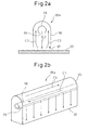
- Fig. 2a is a sectional schematic illustration showing the cleaning nozzle.
- Fig. 2b is a perspective schematic illustration showing the cleaning nozzle shown in Fig. 2a.
- an opening 97 is formed in a direction perpendicular to the moving direction of the table.
- a pipe line 98 extends in the same direction.
- an opening 99 is formed in the same direction.
- the opening 97 of the housing 96 and the opening 99 of the pipe line 98 are formed on the same side.
- cleaning fluid for example, dry air
- this cleaning fluid is injected from the opening 99 along the pipe line 98.
- the cleaning fluid flows out from the housing 96 through the opening 97 as shown by arrow C2.
- the cleaning fluid collides with the wafer 20 and the mount frame 36 located under the cleaning nozzle 95a.
- the wafer 20 and others are then cleaned.
- the cleaning fluid rises along an inner wall of the housing 96 as shown by arrow C3 and flows in the housing 96 in the direction of arrow C4 and is then recovered.
- the wafer 20 and the mount frame 36 on the first support table 71 can be cleaned by the first cleaning nozzle 95a.
- the back surface 22 of the wafer 20 can be cleaned by the first cleaning nozzle 95a. Since the back surface 22 of the wafer 20 is a ground surface, which was ground by the back-grinder 1, there is a possibility that grinding chips may be attached to the back surface, 22 of the wafer 20. However, when the back surface 22 is cleaned by the cleaning nozzle 95a before the dicing tape 3 is adhered, the grinding chips are dispersed. Accordingly, the dicing tape 3 can be adhered to the back surface 22. Due to the foregoing, the adhesive force of the dicing tape 3 can be enhanced.
- the dicing tape adhering unit 30 includes a adhering roller 35. By the adhering roller 35, the dicing tape 3 is adhered to the wafer 20 and the mount frame 36 by a well-known method.
- a cutting portion (not shown) is driven.
- the dicing tape 3 is cut into a circle along the front surface of the mount frame 36.
- a hole the shape of which corresponds to the outline of the mount frame 36, is formed on the dicing tape 3.
- the cutting portion is not used.
- a winding roller 41 of a surplus dicing tape winding unit 40 is driven to mind a surplus dicing tape 3 by a well-known method. Due to the foregoing, the wafer 20 and the mount frame 36 are integrated with each other into one body. Therefore, the wafer 20 and the mount frame 36 can be easily handled in the next step.
- the wafer 20 and the mount frame 36 which have been integrated with each other by the dicing tape 3, will be referred to as "a workpiece” or "a workpiece 60", hereinafter.
- the workpiece 60 is conveyed from the surplus dicing tape winding unit 40 to the inversion region 75 by the first support table 71.
- the workpiece 60 is inverted upside down by a well-known method.
- the back surface 22 of the wafer 20 is directed downward and the surface protection film 110 on the front surface 21 of the wafer 20, on which the circuit pattern is formed, is directed upward.
- the waiting region 27 is composed in the same manner as that of the first UV irradiation portion 5. Therefore, the waiting region 27 may be used as the second UV irradiation portion as follows.
- a stage 27a of the second UV irradiation portion 27 is made of a transparent hard material. Under the stage 27a, UV irradiation device (not shown) is arranged. In the second UV irradiation device 27, the back surface 22 of the wafer 20, that is, the dicing tape 3 faces to the stage 27a. Accordingly, in the second UV irradiation portion 27, ultraviolet rays are irradiated to the dicing tape 3 through the stage 27a. Since the dicing tape 3 has an ultraviolet ray hardening property, it is hardened when ultraviolet rays are irradiated to the dicing tape 3. Therefore, in the next step of dicing, it is possible to prevent the adhesive agent of the dicing tape 3 from adhering to a dicing blade (not shown).
- the workpiece 60 is supported on the second support table 72.
- the workpiece 60 may be directly supported on the second support table 27 without conducting the aforementioned UV processing.
- the second support table 72 is then moved to the second cleaning nozzle 95b so as to clean the workpiece 60. Since the second cleaning nozzle 95b is composed in the same manner as that of the first cleaning nozzle 95a, explanations are omitted here. Due to the foregoing, in the surface protection film peeling unit 50, the peeling tape 4 can be adhered onto the clean surface protection film 110. Therefore, it is possible to enhance the adhesive force of the peeling tape 4.
- Fig. 3 is a schematic illustration showing a portion of the wafer processing device shown in Fig. 1. As can be seen from Figs. 1 and 3, the cleaned workpiece 60 is conveyed to the surface protection film peeling unit 50 by the second support table 72.
- the surface protection film 110 is peeled off from the wafer 20 by a well-known method. Specifically, the operation is conducted as follows. First, the peeling tape 4 is adhered to the surface protection film 110 on the wafer 20. Next, the peeling tape 4 is wound up. The adhesive force between the peeling tape 4 and the surface protection film 110 is stronger than the adhesive force between the surface protection film 110 and the wafer 20, so that at the time of winding the peeling tape 4, the surface protection film 110 is peeled off from the wafer 20, so that the front surface 21 of the wafer 20 is exposed.
- the second support table 72 is then moved from the surface protection film peeling unit 50 to an optical reading device 18.
- This optical reading device 18 reads out character information, for example, ID number previously formed on the front surface 21 of the wafer.
- the second support table 72 is further moved from the optical reading device 18 to a bar code adhering unit 11.
- the bar code adhering unit 11 makes a new bar code 65 according to the character information which has read out by the optical reading device 18.
- the bar code contains information of types corresponding to the character information that was read out, for example, the bar code contains information necessary for dicing such as a type number of the wafer, a diameter, a thickness and alignment information.
- the bar code adhering unit 11 advances on the workpiece 60 and adheres the bar code 65 at a predetermined position on the workpiece 60.
- the bar code 65 may be adhered onto the dicing tape 3 between the mount frame 36 and the wafer 20.
- the bar code 65 may be directly adhered to the wafer 20.
- the bar code 65 may be adhered to the mount frame 36.
- a peeling operation for peeling the surface protection film 110 in the surface protection film peeling unit 50, a reading operation for reading character information in the optical reading device 18 and a adhering operation for adhering the bar code 65 in the bar code adhering unit 11 are executed in this order. That is, in the wafer processing device 10 of the present invention, it is possible to conduct the peeling operation, the reading operation and the adhering operation without detaching the workpiece 60 from the second support table 72.
- the workpiece 60 since the workpiece 60 is not moved to another support table in the present invention, the workpiece 60 does not undulate. As a result, in the optical reading device 18, it is possible to accurately read out character information on the wafer 20. Therefore, it is possible to avoid failures in reading.
- the bar code adhering unit 11 the bar code 65 can be accurately adhered to the workpiece 60. Therefore, it is possible to avoid failures when adhering the bar code. Especially in the case where the bar code 65 is adhered to the dicing tape 3 as shown in Fig. 4a, the occurrence of a failure in adhering the bar code can be effectively prevented by the present invention.
- the workpieces 60, onto which the bar codes 65 are adhered are successively accommodated in the cassette 16 in the workpiece accommodation region 17a.
- the cassette 16 is conveyed to the cassette taking-out region 17b. After that, the cassette 16 is taken out from the wafer processing device 10 and conveyed to the dicing device 101.
- the bar code reader (not shown) reads out the bar code 65 on the workpiece 60.
- the operation condition of the dicing device 101 is automatically set. Since the bar code 65 is accurately adhered in the present invention, there is no possibility that the bar code reader of the dicing device 101 will fail to read the barcode. After that, according to the operation condition that has been set, the wafer 20 of the workpiece 60 is diced.
- ID information is read out from the workpiece 60 by the optical reading device 18.
- the optical reading device 18 may be excluded when ID information of the workpiece 60 is directly input into the bar code adhering unit 11. It is clear that even the above case is included in the scope of the present invention.
Landscapes
- Container, Conveyance, Adherence, Positioning, Of Wafer (AREA)
- Mechanical Treatment Of Semiconductor (AREA)
Abstract
Description
- The present invention relates to a workpiece processing device for processing a wafer workpiece, on the front surface of which a circuit pattern is formed and a surface protection tape is adhered, integrated with a mount frame into one body by a dicing tape.
- In the field of manufacturing semiconductors, there is a tendency for large-sized wafers to be used year after year. Further, in order to enhance packing density, wafer thickness is reduced. In order to reduce the wafer thickness, back-grinding is conducted on the back surface of a semiconductor wafer. At the time of back-grinding, in order to protect a semiconductor element formed on the front surface of a wafer, a surface protection film is adhered to the front surface of the wafer.
- After back-grinding is complete, the wafer is conveyed to a workpiece processing device. Fig. 5 is a view showing a workpiece processing device of the prior art disclosed in
Japanese Patent Application No. 2006-35159 wafer 20, on thefront surface 21 of which a surfaceprotective film 110 is adhered, is subjected to back-surface grinding by a back-grinder 1 as shown in Fig. 5 and conveyed to aworkpiece processing device 100. - A dicing tape is adhered to the back surface of a
wafer 20 in a dicingtape adhering unit 300, so that thewafer 20 can be integrated with amount frame 36 into one body. After surplus dicing tape has been wound by a surplus dicingtape winding unit 400, thewafer 20 and themount frame 36 are conveyed to a surface protectionfilm peeling unit 500. Thesurface protection film 110 is peeled off thefront surface 21 of thewafer 20 by a well-known method. - The
wafer 20 is then conveyed to astage 270a in theworkpiece processing device 100 and subjected to UV irradiation processing and/or expansion processing. Next, character information previously formed on the front surface of thewafer 20 is read out by an optical reading device (not shown). A bar code corresponding to the thus read character information is adhered to the dicing tape between thewafer 20 and themount frame 36 or adhered to themount frame 36 itself. This bar code contains information necessary for dicing the wafer. Next, thewafer 20 is accommodated in acassette 16 and conveyed to a dicing device (not shown) together with thecassette 16. - In the dicing device, the bar code previously described is read out by a bar code reader (not shown). According to the information of the bar code, the operating condition of the dicing device is automatically set.
- In the workpiece processing device disclosed in
Japanese Patent Application No. 2006-35159 surface protection film 110 has been peeled by the surface protectionfilm peeling unit 500, thewafer 20 is conveyed to a table different from the table (not shown) used for the surface protectionfilm peeling unit 500. Thewafer 20 is then subjected to the bar code adhering processing. - Since the
back surface 22 of thewafer 20 is ground as previously described, the thickness is reduced. Accordingly, when the table for supporting the wafer 20 (and the mount frame 36) is changed after thesurface protection film 110 has been peeled, the dicing tape and/or wafer 20 slighetly undulates. When the dicing tape and/orwafer 20 slightly undulates, it is impossible for the optical reading device to accurately read out the character information of the wafer. Accordingly, an error occurs when the character information on the wafer is read. Further, in the case where the bar code is adhered to thedicing tape 3 between thewafer 20 and themount frame 36, it becomes difficult to adhere the bar code. - In this case, in the dicing step, which is an after-step, it is impossible to appropriately set the operating condition of the dicing device according to the bar code. As a result, yield is lowered or working time is delayed.
- The present invention has been accomplished in view of the above circumstances. An object of the present invention is to provide a workpiece processing device capable of avoiding failures when adhering a bar code.
- In order to accomplish the above object, the first aspect provides a workpiece processing device for processing a workpiece comprising: a surface protection film peeling means for peeling a surface protection film, which is adhered to a front surface of the workpiece, with a peeling tape; a bar code adhering means for adhering a bar code corresponding to the workpiece to the workpiece; and a movable support table for supporting the workpiece, wherein a peeling operation for peeling the surface protection film conducted by the surface protection film peeling means and a adhering operation for adhering a bar code conducted by the bar code adhering means are given to the workpiece while the workpiece is being supported by the support table.
- In the first aspect, after the surface protection film has been peeled from the wafer on the support table, without releasing the suction operation of the workpiece, the bar code adhering operation is conducted on the workpiece on the same support table. That is, it is not necessary to move the workpiece from the support table to another support table between the surface protection film peeling operation and the bar code adhering operation. Since the support table is not changed, it is possible to prevent the workpiece from undulating. As a result, the bar code can be appropriately adhered to the workpiece. Accordingly, it is possible to avoid failures when adhering the bar code. In this connection, the terminology of the workpiece includes both a single body of a wafer and a body in which the wafer and the mount frame are integrated with each other by the dicing tape.
- According to the second aspect, as in the first aspect, a workpiece processing device further comprises: an optical reading means for reading out character information previously formed on the workpiece, which is arranged between the surface protection film peeling means and the bar code adhering means, wherein the bar code adhering means adheres a bar code, which corresponds to character information of the workpiece that has been read out by the optical reading means, onto the workpiece, and the workpiece is read by the optical reading means while the workpiece is being supported by the support table.
- In the second aspect, it is possible to avoid failures in reading character information on the wafer.
- According to the third aspect, as in the first or the second aspect, a workpiece processing device further comprises a cleaning means for cleaning the workpiece, arranged in the upstream of the surface protection film peeling means in a moving direction of the support table.
- In the third aspect, after the workpiece has been cleaned by the cleaning means, the surface protection film is peeled. Due to the foregoing, the adhesive force between the peeling tape and the surface protection film is enhanced, so that failure of adhering the peeling tape can be prevented.
- These and other objects, features and advantages of the present invention will be more apparent in light of the detailed description of exemplary embodiments thereof as illustrated by the drawings.
- In the drawings:
- Fig. 1 is a top view showing a wafer processing device according to the present invention;
- Fig. 2a is a sectional schematic illustration showing a cleaning nozzle;
- Fig. 2b is a perspective schematic illustration showing the cleaning nozzle shown in Fig. 2a;
- Fig. 3 is a schematic illustration showing a portion of the wafer processing device shown in Fig. 1;
- Fig. 4a is a view showing a adhering position of a bar code on a workpiece;
- Fig. 4b is another view showing a adhering position of a bar code on a workpiece; and
- Fig. 5 is a top view showing a wafer processing device of the prior art.
- Referring to the accompanying drawings, an embodiment of the present invention will be explained below. Like reference numerals are used to indicate like parts in the following drawings. In order to facilitate understanding, the reduced scale used in these drawings has been appropriately changed.
- Fig. 1 is a plan view showing a wafer processing device according to the present invention. In Fig. 1, a
wafer processing device 10 is arranged adjacent to a back-grinder 1. As shown in Fig. 1, thiswafer processing device 10 is connected to the back-grinder 1 by a first UV irradiation portion 5 (ultraviolet ray irradiation portion). - In a
housing 12 of thewafer processing device 10 shown in Fig. 1, a mountframe arrangement portion 15, in which a plurality of mount frames 36 are arranged, is provided. In thishousing 12, acassette region 17 for acassette 16, in whichwafers 20 integrated with the mount frames 36 are accommodated, is arranged adjacent to the mountframe arrangement portion 15. Further, in Fig. 1, a barcode adhering unit 11 for adhering a bar code label is arranged on front of thecassette region 17 in thehousing 12. - In the
wafer processing device 10 shown in Fig. 1, a first support table 71 for supporting thewafer 20 and themount frame 36 is arranged in the longitudinal direction of thehousing 12. - As shown in the drawing, a
first cleaning nozzle 95a, a dicingtape adhering unit 30 and a surplus dicingtape winding unit 40 are arranged in this order in a movement passage of the first support table 71 when a view is taken from the mountframe arrangement portion 15 side. The movement passage of the first support table 71 ends at aninversion region 75. - As shown in Fig. 1, a waiting
region 27 is provided adjacent to theinversion region 75. In the initial stage, a second support table 72, which is arranged in the waitingregion 27, can be moved in the longitudinal direction in the opposite direction to the first support table 71. As shown in the drawing, asecond cleaning nozzle 95b, a surface protectionfilm peeling unit 50, anoptical reading device 18 and a barcode adhering unit 11 are arranged in this order in a movement passage of the second support table 72 when a view is taken from the waitingregion 27 side. - As shown in the drawing, a
cassette region 17 includes: aworkpiece accommodation region 17a for accommodating thewafer 20 and others on the second support table 72 into thecassette 16; and a cassette taking-out region 17b for taking out thecassette 16, in which a plurality ofwafers 20 and others are accommodated, from thewafer processing device 10. As can be seen from Fig. 1, the movement passage of the second support table 72 ends in front of thecassette 16 arranged in thework accommodation region 17a. - Although not shown in the drawing, the
wafer processing device 10 of the present invention includes a control portion, such as a digital computer. Each element of thewafer processing device 10 is connected to and controlled by the control portion. The operation of thewafer processing device 10 of the present invention will be explained below. - First of all, under the condition that a
surface protection film 110 for protecting a circuit pattern formed on a front surface of the wafer is adhered to thefront surface 21, thewafer 20 is supplied to the back-grinder 1. In the back-grinder 1, under the condition that thesurface protection film 110 on thefront surface 21 of thewafer 20 is sucked, aback surface 22 of thewafer 20 is ground by a well known method. Due to the foregoing, thewafer 20 is ground and the thickness of thewafer 20 is reduced to, for example, 50 micrometers or less. Next, while theback surface 22 of thewafer 20, that is, aground face 22 of thewafer 20 is being held, thewafer 20 is supplied toUV irradiation portion 5. - A
stage 5a of the firstUV irradiation portion 5 for connecting the back-grinder 1 with thewafer processing device 10 is made of transparent hard material. Under thestage 5a, UV irradiation device not shown is arranged. When the wafer passes through the firstUV irradiation portion 5, thefront surface 21 of thewafer 20, that is, thesurface protection film 110 faces thestage 5a of theUV irradiation portion 5. At this time, thesurface protection film 110 is irradiated with UV by the firstUV irradiation portion 5 through thestage 5a. Due to the foregoing, thesurface protection film 110 is hardened. Therefore, the adhesion of thesurface protection film 110 to thefront surface 21 of thewafer 20 is somewhat reduced. Accordingly, thesurface protection film 110 can be easily peeled off as described later. - In the case where the
surface protection film 110 has no ultraviolet ray hardening property, an irradiating operation is not conducted in the first UVray irradiation portion 5, and thewafer 20 merely passes throughUV irradiation portion 5. - After the
wafer 20 has passed through the firstUV irradiation portion 5, it is conveyed to the first support table 71 of thewafer processing device 10 by a robot hand (not shown in the drawing). Then, thewafer 20 is sucked to and held by the support table 71. That is, thesurface protection film 110 of thewafer 20 is held by the first support table 71 and theback surface 22 of thewafer 20 is exposed. Onemount frame 36 is conveyed from the mountframe arrangement portion 15 to the first support table 71 and sucked to and held by the support table 71 in the same manner. - First, the first support table 71 is moved to the
first cleaning nozzle 95a so as to clean thewafer 20 and themount frame 36. The cleaningnozzle 95a extends in a direction perpendicular to the moving direction of the first support table 71 in a range of at least the diameter of thewafer 20, preferably in a range exceeding the diameter of themount frame 36. - Fig. 2a is a sectional schematic illustration showing the cleaning nozzle. Fig. 2b is a perspective schematic illustration showing the cleaning nozzle shown in Fig. 2a. As shown in these drawings, in a lower portion of the
housing 96 of the cleaningnozzle 95a, anopening 97 is formed in a direction perpendicular to the moving direction of the table. Further, in thehousing 96, apipe line 98 extends in the same direction. In a lower portion of thepipe line 98 facing to theopening 97, anopening 99 is formed in the same direction. As shown in the drawing, theopening 97 of thehousing 96 and theopening 99 of thepipe line 98 are formed on the same side. - As shown in Figs. 2a and 2b, when cleaning fluid, for example, dry air is made to flow in the
pipe line 98 in the direction of arrow C1, this cleaning fluid is injected from theopening 99 along thepipe line 98. The cleaning fluid flows out from thehousing 96 through theopening 97 as shown by arrow C2. After the cleaning fluid has flowed out from thehousing 96, it collides with thewafer 20 and themount frame 36 located under the cleaningnozzle 95a. Thewafer 20 and others are then cleaned. Then the cleaning fluid rises along an inner wall of thehousing 96 as shown by arrow C3 and flows in thehousing 96 in the direction of arrow C4 and is then recovered. - Before the dicing
tape 3 is adhered, thewafer 20 and themount frame 36 on the first support table 71 can be cleaned by thefirst cleaning nozzle 95a. Especially, theback surface 22 of thewafer 20 can be cleaned by thefirst cleaning nozzle 95a. Since theback surface 22 of thewafer 20 is a ground surface, which was ground by the back-grinder 1, there is a possibility that grinding chips may be attached to the back surface, 22 of thewafer 20. However, when theback surface 22 is cleaned by the cleaningnozzle 95a before the dicingtape 3 is adhered, the grinding chips are dispersed. Accordingly, the dicingtape 3 can be adhered to theback surface 22. Due to the foregoing, the adhesive force of the dicingtape 3 can be enhanced. - After the cleaning has been completed by the
first cleaning nozzle 95a, thewafer 20 and themount frame 36 are supplied to the dicingtape adhering unit 30 by the first support table 71. The dicingtape adhering unit 30 includes a adheringroller 35. By the adheringroller 35, the dicingtape 3 is adhered to thewafer 20 and themount frame 36 by a well-known method. - Then a cutting portion (not shown) is driven. By this cutting portion, the dicing
tape 3 is cut into a circle along the front surface of themount frame 36. As a result, a hole, the shape of which corresponds to the outline of themount frame 36, is formed on the dicingtape 3. In this connection, in the case where a dicingtape 3, which has previously been subjected to punching, is used, the cutting portion is not used. - Next, a winding
roller 41 of a surplus dicingtape winding unit 40 is driven to mind asurplus dicing tape 3 by a well-known method. Due to the foregoing, thewafer 20 and themount frame 36 are integrated with each other into one body. Therefore, thewafer 20 and themount frame 36 can be easily handled in the next step. In the present invention, thewafer 20 and themount frame 36, which have been integrated with each other by the dicingtape 3, will be referred to as "a workpiece" or "aworkpiece 60", hereinafter. - The
workpiece 60 is conveyed from the surplus dicingtape winding unit 40 to theinversion region 75 by the first support table 71. In theinversion region 75, theworkpiece 60 is inverted upside down by a well-known method. As a result, theback surface 22 of thewafer 20 is directed downward and thesurface protection film 110 on thefront surface 21 of thewafer 20, on which the circuit pattern is formed, is directed upward. - Then the
workpiece 60 is conveyed from the first support table 71 to a waitingregion 27 by a robot hand (not shown). The waitingregion 27 is composed in the same manner as that of the firstUV irradiation portion 5. Therefore, the waitingregion 27 may be used as the second UV irradiation portion as follows. - That is, a stage 27a of the second
UV irradiation portion 27 is made of a transparent hard material. Under the stage 27a, UV irradiation device (not shown) is arranged. In the secondUV irradiation device 27, theback surface 22 of thewafer 20, that is, the dicingtape 3 faces to the stage 27a. Accordingly, in the secondUV irradiation portion 27, ultraviolet rays are irradiated to the dicingtape 3 through the stage 27a. Since the dicingtape 3 has an ultraviolet ray hardening property, it is hardened when ultraviolet rays are irradiated to the dicingtape 3. Therefore, in the next step of dicing, it is possible to prevent the adhesive agent of the dicingtape 3 from adhering to a dicing blade (not shown). - After that, the
workpiece 60 is supported on the second support table 72. In this connection, theworkpiece 60 may be directly supported on the second support table 27 without conducting the aforementioned UV processing. - The second support table 72 is then moved to the
second cleaning nozzle 95b so as to clean theworkpiece 60. Since thesecond cleaning nozzle 95b is composed in the same manner as that of thefirst cleaning nozzle 95a, explanations are omitted here. Due to the foregoing, in the surface protectionfilm peeling unit 50, the peeling tape 4 can be adhered onto the cleansurface protection film 110. Therefore, it is possible to enhance the adhesive force of the peeling tape 4. - Fig. 3 is a schematic illustration showing a portion of the wafer processing device shown in Fig. 1. As can be seen from Figs. 1 and 3, the cleaned
workpiece 60 is conveyed to the surface protectionfilm peeling unit 50 by the second support table 72. - In the surface protection
film peeling unit 50, thesurface protection film 110 is peeled off from thewafer 20 by a well-known method. Specifically, the operation is conducted as follows. First, the peeling tape 4 is adhered to thesurface protection film 110 on thewafer 20. Next, the peeling tape 4 is wound up. The adhesive force between the peeling tape 4 and thesurface protection film 110 is stronger than the adhesive force between thesurface protection film 110 and thewafer 20, so that at the time of winding the peeling tape 4, thesurface protection film 110 is peeled off from thewafer 20, so that thefront surface 21 of thewafer 20 is exposed. - The second support table 72 is then moved from the surface protection
film peeling unit 50 to anoptical reading device 18. Thisoptical reading device 18 reads out character information, for example, ID number previously formed on thefront surface 21 of the wafer. - After that, the second support table 72 is further moved from the
optical reading device 18 to a barcode adhering unit 11. The barcode adhering unit 11 makes anew bar code 65 according to the character information which has read out by theoptical reading device 18. The bar code contains information of types corresponding to the character information that was read out, for example, the bar code contains information necessary for dicing such as a type number of the wafer, a diameter, a thickness and alignment information. - The bar
code adhering unit 11 advances on theworkpiece 60 and adheres thebar code 65 at a predetermined position on theworkpiece 60. As shown in Figs. 4a and 4b, thebar code 65 may be adhered onto the dicingtape 3 between themount frame 36 and thewafer 20. Alternatively, thebar code 65 may be directly adhered to thewafer 20. In this connection, although not shown in the drawing, thebar code 65 may be adhered to themount frame 36. - As can be seen from Fig. 3, in the present invention, by moving the second support table 72, a peeling operation for peeling the
surface protection film 110 in the surface protectionfilm peeling unit 50, a reading operation for reading character information in theoptical reading device 18 and a adhering operation for adhering thebar code 65 in the barcode adhering unit 11 are executed in this order. That is, in thewafer processing device 10 of the present invention, it is possible to conduct the peeling operation, the reading operation and the adhering operation without detaching the workpiece 60 from the second support table 72. - That is, since the
workpiece 60 is not moved to another support table in the present invention, theworkpiece 60 does not undulate. As a result, in theoptical reading device 18, it is possible to accurately read out character information on thewafer 20. Therefore, it is possible to avoid failures in reading. In the same manner, in the barcode adhering unit 11, thebar code 65 can be accurately adhered to theworkpiece 60. Therefore, it is possible to avoid failures when adhering the bar code. Especially in the case where thebar code 65 is adhered to the dicingtape 3 as shown in Fig. 4a, the occurrence of a failure in adhering the bar code can be effectively prevented by the present invention. - Referring to Fig. 1 again, the
workpieces 60, onto which thebar codes 65 are adhered, are successively accommodated in thecassette 16 in theworkpiece accommodation region 17a. After a predetermined number ofworkpieces 60 have been accommodated in thecassette 16, thecassette 16 is conveyed to the cassette taking-out region 17b. After that, thecassette 16 is taken out from thewafer processing device 10 and conveyed to thedicing device 101. - In the
dicing device 101, the bar code reader (not shown) reads out thebar code 65 on theworkpiece 60. Next, according to the information of a type recorded in the bar code, the operation condition of thedicing device 101 is automatically set. Since thebar code 65 is accurately adhered in the present invention, there is no possibility that the bar code reader of thedicing device 101 will fail to read the barcode. After that, according to the operation condition that has been set, thewafer 20 of theworkpiece 60 is diced. - In the embodiment explained above referring to the drawings, ID information is read out from the
workpiece 60 by theoptical reading device 18. However, theoptical reading device 18 may be excluded when ID information of theworkpiece 60 is directly input into the barcode adhering unit 11. It is clear that even the above case is included in the scope of the present invention.
Claims (3)
- A workpiece processing device for processing a workpiece comprising:a surface protection film peeling means for peeling a surface protection film, which is adhered onto a front surface of the workpiece, with a peeling tape;a bar code adhering means for adhering a bar code corresponding to the workpiece to the workpiece; anda movable support table for supporting the workpiece, whereina peeling operation for peeling the surface protection film conducted by the surface protection film peeling means and a adhering operation for adhering a bar code conducted by the bar code adhering means are given to the workpiece while the workpiece is being supported by the support table.
- A workpiece processing device according to claim 1, further comprising
an optical reading means for reading out character information previously formed on the workpiece, which is arranged between the surface protection film peeling means and the bar code adhering means, wherein
the bar code adhering means adheres a bar code, which corresponds to character information of the workpiece that has been read out by the optical reading means, to the workpiece, and
the workpiece is given a reading operation conducted by the optical reading means while the workpiece is being supported by the support table. - A workpiece processing device according to claim 1 or 2, further comprising a cleaning means for cleaning the workpiece, arranged in the upstream of the surface protection film peeling means in a moving direction of the support table.
Applications Claiming Priority (1)
| Application Number | Priority Date | Filing Date | Title |
|---|---|---|---|
| JP2006155921A JP4693696B2 (en) | 2006-06-05 | 2006-06-05 | Work processing device |
Publications (2)
| Publication Number | Publication Date |
|---|---|
| EP1865535A2 true EP1865535A2 (en) | 2007-12-12 |
| EP1865535A3 EP1865535A3 (en) | 2009-08-12 |
Family
ID=38327061
Family Applications (1)
| Application Number | Title | Priority Date | Filing Date |
|---|---|---|---|
| EP07109098A Withdrawn EP1865535A3 (en) | 2006-06-05 | 2007-05-29 | Workpiece processing device |
Country Status (6)
| Country | Link |
|---|---|
| US (1) | US7490650B2 (en) |
| EP (1) | EP1865535A3 (en) |
| JP (1) | JP4693696B2 (en) |
| KR (1) | KR100861424B1 (en) |
| SG (1) | SG137831A1 (en) |
| TW (1) | TWI337759B (en) |
Families Citing this family (12)
| Publication number | Priority date | Publication date | Assignee | Title |
|---|---|---|---|---|
| JP4841262B2 (en) * | 2006-02-13 | 2011-12-21 | 株式会社東京精密 | Wafer processing equipment |
| TW201015652A (en) * | 2008-10-07 | 2010-04-16 | Asia Ic Mic Process Inc | Separating device and method |
| JP5957220B2 (en) * | 2011-12-20 | 2016-07-27 | 株式会社ディスコ | Method for judging cracks in plate-like workpieces |
| WO2016046952A1 (en) * | 2014-09-26 | 2016-03-31 | 富士機械製造株式会社 | Wafer transfer apparatus |
| JP6427131B2 (en) | 2016-03-18 | 2018-11-21 | 株式会社荏原製作所 | Polishing apparatus and polishing method |
| JP6692577B2 (en) * | 2016-06-24 | 2020-05-13 | 株式会社ディスコ | Wafer processing method |
| JP6842352B2 (en) * | 2017-04-25 | 2021-03-17 | 株式会社ディスコ | How to protect barcode stickers |
| JP6858452B2 (en) * | 2017-06-23 | 2021-04-14 | 株式会社ディスコ | Wafer jig with identification mark |
| WO2019013022A1 (en) * | 2017-07-12 | 2019-01-17 | 東京エレクトロン株式会社 | Conveyance device, substrate processing system, conveyance method, and substrate processing method |
| WO2019044506A1 (en) * | 2017-08-28 | 2019-03-07 | 東京エレクトロン株式会社 | Substrate processing system, and substrate processing method |
| JP7379234B2 (en) * | 2020-03-24 | 2023-11-14 | リンテック株式会社 | Sheet peeling device and sheet peeling method |
| JP7754679B2 (en) * | 2021-10-19 | 2025-10-15 | 株式会社ディスコ | processing equipment |
Family Cites Families (22)
| Publication number | Priority date | Publication date | Assignee | Title |
|---|---|---|---|---|
| JPS60100450A (en) * | 1983-11-07 | 1985-06-04 | Disco Abrasive Sys Ltd | Semiconductor wafer mounting and cutting system |
| JPS628966A (en) | 1985-07-05 | 1987-01-16 | Nitto Electric Ind Co Ltd | Method and device of sticking wafer and ring frame |
| US5118369A (en) * | 1990-08-23 | 1992-06-02 | Colorcode Unlimited Corporation | Microlabelling system and process for making microlabels |
| JPH097977A (en) * | 1995-06-26 | 1997-01-10 | Disco Abrasive Syst Ltd | Dicing device and dicing system |
| JP3171148B2 (en) | 1997-09-01 | 2001-05-28 | 日本電気株式会社 | Wafer mount device |
| JP3888754B2 (en) * | 1997-12-08 | 2007-03-07 | 日東電工株式会社 | Automatic semiconductor wafer pasting equipment |
| JP3560823B2 (en) | 1998-08-18 | 2004-09-02 | リンテック株式会社 | Wafer transfer device |
| US6191037B1 (en) * | 1998-09-03 | 2001-02-20 | Micron Technology, Inc. | Methods, apparatuses and substrate assembly structures for fabricating microelectronic components using mechanical and chemical-mechanical planarization processes |
| KR20020026668A (en) * | 2000-10-02 | 2002-04-12 | 윤종용 | Method for labelling a semiconductor wafer |
| JP2002343756A (en) | 2001-05-21 | 2002-11-29 | Tokyo Seimitsu Co Ltd | Wafer flat surface processing equipment |
| JP4748901B2 (en) * | 2001-09-06 | 2011-08-17 | 日東電工株式会社 | Semiconductor wafer mounting method and cassette used therefor |
| JP3837320B2 (en) | 2001-11-07 | 2006-10-25 | リンテック株式会社 | Optical disc laminating device |
| JP4201564B2 (en) * | 2001-12-03 | 2008-12-24 | 日東電工株式会社 | Semiconductor wafer transfer method and semiconductor wafer transfer apparatus using the same |
| JP3989354B2 (en) * | 2002-10-11 | 2007-10-10 | リンテック株式会社 | Bonding device |
| JP2004363165A (en) * | 2003-06-02 | 2004-12-24 | Tokyo Seimitsu Co Ltd | Wafer processing apparatus and wafer processing method |
| US7158910B2 (en) * | 2003-07-15 | 2007-01-02 | Tokyo Seimitsu Co., Ltd. | Device for calculating the quantity of light and method thereof |
| JP4485248B2 (en) | 2004-04-28 | 2010-06-16 | リンテック株式会社 | Peeling apparatus and peeling method |
| JP2006035159A (en) | 2004-07-29 | 2006-02-09 | Japan Organo Co Ltd | Electrochemical water treatment method and apparatus |
| JP2006100728A (en) * | 2004-09-30 | 2006-04-13 | Nitto Denko Corp | Protective tape peeling method and apparatus using the same |
| JP4326519B2 (en) * | 2005-03-31 | 2009-09-09 | 日東電工株式会社 | Protective tape peeling method and apparatus using the same |
| JP4541237B2 (en) * | 2005-06-29 | 2010-09-08 | リンテック株式会社 | Semiconductor wafer processing tape winding body, semiconductor wafer processing tape sticking apparatus using the same, and semiconductor wafer processing apparatus |
| JP4841262B2 (en) * | 2006-02-13 | 2011-12-21 | 株式会社東京精密 | Wafer processing equipment |
-
2006
- 2006-06-05 JP JP2006155921A patent/JP4693696B2/en active Active
-
2007
- 2007-05-22 TW TW096118215A patent/TWI337759B/en not_active IP Right Cessation
- 2007-05-22 US US11/752,146 patent/US7490650B2/en active Active
- 2007-05-29 EP EP07109098A patent/EP1865535A3/en not_active Withdrawn
- 2007-05-30 SG SG200703938-1A patent/SG137831A1/en unknown
- 2007-06-04 KR KR1020070054635A patent/KR100861424B1/en not_active Expired - Fee Related
Also Published As
| Publication number | Publication date |
|---|---|
| SG137831A1 (en) | 2007-12-28 |
| KR20070116560A (en) | 2007-12-10 |
| TW200807535A (en) | 2008-02-01 |
| JP4693696B2 (en) | 2011-06-01 |
| JP2007324516A (en) | 2007-12-13 |
| US7490650B2 (en) | 2009-02-17 |
| US20070277934A1 (en) | 2007-12-06 |
| KR100861424B1 (en) | 2008-10-07 |
| EP1865535A3 (en) | 2009-08-12 |
| TWI337759B (en) | 2011-02-21 |
Similar Documents
| Publication | Publication Date | Title |
|---|---|---|
| US7490650B2 (en) | Workpiece processing device | |
| US6943094B2 (en) | Method for attaching semiconductor components to a substrate using component attach system having radiation exposure assembly | |
| CN101131921B (en) | Wafer processing method | |
| JP2005101290A (en) | Semiconductor wafer dividing method | |
| US20030088959A1 (en) | Wafer transfer apparatus | |
| KR102581316B1 (en) | Transport equipment, substrate processing system, transport method and substrate processing method | |
| CN105097637B (en) | Method for processing wafer | |
| CN101807542A (en) | Wafer processing method | |
| KR102227406B1 (en) | Wafer processing system | |
| KR20180123018A (en) | Substrate transfer method and substrate transfer apparatus | |
| KR20000077293A (en) | Method of processing semiconductor wafer and semiconductor wafer supporting member | |
| JP4324788B2 (en) | Wafer mounter | |
| JP4505789B2 (en) | Chip manufacturing method | |
| CN101556910B (en) | Processer | |
| CN104022012A (en) | Adhesive tape cutting method and adhesive tape cutting apparatus | |
| JP4565977B2 (en) | Film peeling method and film peeling apparatus | |
| EP1947688A1 (en) | Film peeling method and film peeling apparatus | |
| JP2019021703A (en) | Cutting method for plate workpiece | |
| JP2008293508A (en) | Semiconductor wafer machining method and semiconductor wafer support member | |
| EP1054437A2 (en) | Method and apparatus for attaching wafer to wafer frame and planarization apparatus including attaching apparatus | |
| US6946311B2 (en) | Processing apparatus and wafer processing method | |
| KR102898202B1 (en) | Machining apparatus and method for using machining apparatus | |
| TWI267913B (en) | Wafer dicing method | |
| JP2002353170A (en) | Semiconductor wafer separation system, separation method and dicing apparatus | |
| JPH04367250A (en) | Manufacture of semiconductor chip |
Legal Events
| Date | Code | Title | Description |
|---|---|---|---|
| PUAI | Public reference made under article 153(3) epc to a published international application that has entered the european phase |
Free format text: ORIGINAL CODE: 0009012 |
|
| 17P | Request for examination filed |
Effective date: 20070615 |
|
| AK | Designated contracting states |
Kind code of ref document: A2 Designated state(s): AT BE BG CH CY CZ DE DK EE ES FI FR GB GR HU IE IS IT LI LT LU LV MC MT NL PL PT RO SE SI SK TR |
|
| AX | Request for extension of the european patent |
Extension state: AL BA HR MK YU |
|
| PUAL | Search report despatched |
Free format text: ORIGINAL CODE: 0009013 |
|
| AK | Designated contracting states |
Kind code of ref document: A3 Designated state(s): AT BE BG CH CY CZ DE DK EE ES FI FR GB GR HU IE IS IT LI LT LU LV MC MT NL PL PT RO SE SI SK TR |
|
| AX | Request for extension of the european patent |
Extension state: AL BA HR MK RS |
|
| AKX | Designation fees paid |
Designated state(s): DE FR GB IT NL |
|
| STAA | Information on the status of an ep patent application or granted ep patent |
Free format text: STATUS: THE APPLICATION IS DEEMED TO BE WITHDRAWN |
|
| 18D | Application deemed to be withdrawn |
Effective date: 20100216 |