EP1865545A1 - Bande adhesive pour decoupage en des de tranches et procede de fabrication de puces l utilisant - Google Patents
Bande adhesive pour decoupage en des de tranches et procede de fabrication de puces l utilisant Download PDFInfo
- Publication number
- EP1865545A1 EP1865545A1 EP06730257A EP06730257A EP1865545A1 EP 1865545 A1 EP1865545 A1 EP 1865545A1 EP 06730257 A EP06730257 A EP 06730257A EP 06730257 A EP06730257 A EP 06730257A EP 1865545 A1 EP1865545 A1 EP 1865545A1
- Authority
- EP
- European Patent Office
- Prior art keywords
- removable adhesive
- adhesive layer
- radiation
- wafer
- dicing
- Prior art date
- Legal status (The legal status is an assumption and is not a legal conclusion. Google has not performed a legal analysis and makes no representation as to the accuracy of the status listed.)
- Withdrawn
Links
Images

Classifications
-
- H—ELECTRICITY
- H10—SEMICONDUCTOR DEVICES; ELECTRIC SOLID-STATE DEVICES NOT OTHERWISE PROVIDED FOR
- H10P—GENERIC PROCESSES OR APPARATUS FOR THE MANUFACTURE OR TREATMENT OF DEVICES COVERED BY CLASS H10
- H10P72/00—Handling or holding of wafers, substrates or devices during manufacture or treatment thereof
- H10P72/04—Apparatus for manufacture or treatment
- H10P72/0442—Apparatus for placing on an insulating substrate, e.g. tape
-
- H—ELECTRICITY
- H10—SEMICONDUCTOR DEVICES; ELECTRIC SOLID-STATE DEVICES NOT OTHERWISE PROVIDED FOR
- H10P—GENERIC PROCESSES OR APPARATUS FOR THE MANUFACTURE OR TREATMENT OF DEVICES COVERED BY CLASS H10
- H10P95/00—Generic processes or apparatus for manufacture or treatments not covered by the other groups of this subclass
-
- C—CHEMISTRY; METALLURGY
- C09—DYES; PAINTS; POLISHES; NATURAL RESINS; ADHESIVES; COMPOSITIONS NOT OTHERWISE PROVIDED FOR; APPLICATIONS OF MATERIALS NOT OTHERWISE PROVIDED FOR
- C09J—ADHESIVES; NON-MECHANICAL ASPECTS OF ADHESIVE PROCESSES IN GENERAL; ADHESIVE PROCESSES NOT PROVIDED FOR ELSEWHERE; USE OF MATERIALS AS ADHESIVES
- C09J4/00—Adhesives based on organic non-macromolecular compounds having at least one polymerisable carbon-to-carbon unsaturated bond ; adhesives, based on monomers of macromolecular compounds of groups C09J183/00 - C09J183/16
-
- C—CHEMISTRY; METALLURGY
- C09—DYES; PAINTS; POLISHES; NATURAL RESINS; ADHESIVES; COMPOSITIONS NOT OTHERWISE PROVIDED FOR; APPLICATIONS OF MATERIALS NOT OTHERWISE PROVIDED FOR
- C09J—ADHESIVES; NON-MECHANICAL ASPECTS OF ADHESIVE PROCESSES IN GENERAL; ADHESIVE PROCESSES NOT PROVIDED FOR ELSEWHERE; USE OF MATERIALS AS ADHESIVES
- C09J7/00—Adhesives in the form of films or foils
- C09J7/20—Adhesives in the form of films or foils characterised by their carriers
- C09J7/22—Plastics; Metallised plastics
-
- C—CHEMISTRY; METALLURGY
- C09—DYES; PAINTS; POLISHES; NATURAL RESINS; ADHESIVES; COMPOSITIONS NOT OTHERWISE PROVIDED FOR; APPLICATIONS OF MATERIALS NOT OTHERWISE PROVIDED FOR
- C09J—ADHESIVES; NON-MECHANICAL ASPECTS OF ADHESIVE PROCESSES IN GENERAL; ADHESIVE PROCESSES NOT PROVIDED FOR ELSEWHERE; USE OF MATERIALS AS ADHESIVES
- C09J7/00—Adhesives in the form of films or foils
- C09J7/30—Adhesives in the form of films or foils characterised by the adhesive composition
- C09J7/38—Pressure-sensitive adhesives [PSA]
-
- C—CHEMISTRY; METALLURGY
- C09—DYES; PAINTS; POLISHES; NATURAL RESINS; ADHESIVES; COMPOSITIONS NOT OTHERWISE PROVIDED FOR; APPLICATIONS OF MATERIALS NOT OTHERWISE PROVIDED FOR
- C09J—ADHESIVES; NON-MECHANICAL ASPECTS OF ADHESIVE PROCESSES IN GENERAL; ADHESIVE PROCESSES NOT PROVIDED FOR ELSEWHERE; USE OF MATERIALS AS ADHESIVES
- C09J7/00—Adhesives in the form of films or foils
- C09J7/30—Adhesives in the form of films or foils characterised by the adhesive composition
- C09J7/38—Pressure-sensitive adhesives [PSA]
- C09J7/381—Pressure-sensitive adhesives [PSA] based on macromolecular compounds obtained by reactions involving only carbon-to-carbon unsaturated bonds
- C09J7/385—Acrylic polymers
-
- H—ELECTRICITY
- H10—SEMICONDUCTOR DEVICES; ELECTRIC SOLID-STATE DEVICES NOT OTHERWISE PROVIDED FOR
- H10P—GENERIC PROCESSES OR APPARATUS FOR THE MANUFACTURE OR TREATMENT OF DEVICES COVERED BY CLASS H10
- H10P72/00—Handling or holding of wafers, substrates or devices during manufacture or treatment thereof
- H10P72/70—Handling or holding of wafers, substrates or devices during manufacture or treatment thereof for supporting or gripping
- H10P72/74—Handling or holding of wafers, substrates or devices during manufacture or treatment thereof for supporting or gripping using temporarily an auxiliary support
-
- H—ELECTRICITY
- H10—SEMICONDUCTOR DEVICES; ELECTRIC SOLID-STATE DEVICES NOT OTHERWISE PROVIDED FOR
- H10P—GENERIC PROCESSES OR APPARATUS FOR THE MANUFACTURE OR TREATMENT OF DEVICES COVERED BY CLASS H10
- H10P72/00—Handling or holding of wafers, substrates or devices during manufacture or treatment thereof
- H10P72/70—Handling or holding of wafers, substrates or devices during manufacture or treatment thereof for supporting or gripping
- H10P72/74—Handling or holding of wafers, substrates or devices during manufacture or treatment thereof for supporting or gripping using temporarily an auxiliary support
- H10P72/7402—Wafer tapes, e.g. grinding or dicing support tapes
-
- H—ELECTRICITY
- H10—SEMICONDUCTOR DEVICES; ELECTRIC SOLID-STATE DEVICES NOT OTHERWISE PROVIDED FOR
- H10P—GENERIC PROCESSES OR APPARATUS FOR THE MANUFACTURE OR TREATMENT OF DEVICES COVERED BY CLASS H10
- H10P72/00—Handling or holding of wafers, substrates or devices during manufacture or treatment thereof
- H10P72/70—Handling or holding of wafers, substrates or devices during manufacture or treatment thereof for supporting or gripping
- H10P72/74—Handling or holding of wafers, substrates or devices during manufacture or treatment thereof for supporting or gripping using temporarily an auxiliary support
- H10P72/7402—Wafer tapes, e.g. grinding or dicing support tapes
- H10P72/7404—Wafer tapes, e.g. grinding or dicing support tapes the wafer tape being a laminate of three or more layers, e.g. including additional layers beyond a base layer and an uppermost adhesive layer
-
- C—CHEMISTRY; METALLURGY
- C09—DYES; PAINTS; POLISHES; NATURAL RESINS; ADHESIVES; COMPOSITIONS NOT OTHERWISE PROVIDED FOR; APPLICATIONS OF MATERIALS NOT OTHERWISE PROVIDED FOR
- C09J—ADHESIVES; NON-MECHANICAL ASPECTS OF ADHESIVE PROCESSES IN GENERAL; ADHESIVE PROCESSES NOT PROVIDED FOR ELSEWHERE; USE OF MATERIALS AS ADHESIVES
- C09J2203/00—Applications of adhesives in processes or use of adhesives in the form of films or foils
- C09J2203/326—Applications of adhesives in processes or use of adhesives in the form of films or foils for bonding electronic components such as wafers, chips or semiconductors
-
- C—CHEMISTRY; METALLURGY
- C09—DYES; PAINTS; POLISHES; NATURAL RESINS; ADHESIVES; COMPOSITIONS NOT OTHERWISE PROVIDED FOR; APPLICATIONS OF MATERIALS NOT OTHERWISE PROVIDED FOR
- C09J—ADHESIVES; NON-MECHANICAL ASPECTS OF ADHESIVE PROCESSES IN GENERAL; ADHESIVE PROCESSES NOT PROVIDED FOR ELSEWHERE; USE OF MATERIALS AS ADHESIVES
- C09J2301/00—Additional features of adhesives in the form of films or foils
- C09J2301/20—Additional features of adhesives in the form of films or foils characterized by the structural features of the adhesive itself
- C09J2301/208—Additional features of adhesives in the form of films or foils characterized by the structural features of the adhesive itself the adhesive layer being constituted by at least two or more adjacent or superposed adhesive layers, e.g. multilayer adhesive
-
- H—ELECTRICITY
- H10—SEMICONDUCTOR DEVICES; ELECTRIC SOLID-STATE DEVICES NOT OTHERWISE PROVIDED FOR
- H10P—GENERIC PROCESSES OR APPARATUS FOR THE MANUFACTURE OR TREATMENT OF DEVICES COVERED BY CLASS H10
- H10P72/00—Handling or holding of wafers, substrates or devices during manufacture or treatment thereof
- H10P72/70—Handling or holding of wafers, substrates or devices during manufacture or treatment thereof for supporting or gripping
- H10P72/74—Handling or holding of wafers, substrates or devices during manufacture or treatment thereof for supporting or gripping using temporarily an auxiliary support
- H10P72/7412—Handling or holding of wafers, substrates or devices during manufacture or treatment thereof for supporting or gripping using temporarily an auxiliary support the auxiliary support including means facilitating the separation of a device or wafer from the auxiliary support
- H10P72/7414—Handling or holding of wafers, substrates or devices during manufacture or treatment thereof for supporting or gripping using temporarily an auxiliary support the auxiliary support including means facilitating the separation of a device or wafer from the auxiliary support the auxiliary support including means facilitating the selective separation of some of a plurality of devices from the auxiliary support
-
- H—ELECTRICITY
- H10—SEMICONDUCTOR DEVICES; ELECTRIC SOLID-STATE DEVICES NOT OTHERWISE PROVIDED FOR
- H10P—GENERIC PROCESSES OR APPARATUS FOR THE MANUFACTURE OR TREATMENT OF DEVICES COVERED BY CLASS H10
- H10P72/00—Handling or holding of wafers, substrates or devices during manufacture or treatment thereof
- H10P72/70—Handling or holding of wafers, substrates or devices during manufacture or treatment thereof for supporting or gripping
- H10P72/74—Handling or holding of wafers, substrates or devices during manufacture or treatment thereof for supporting or gripping using temporarily an auxiliary support
- H10P72/7416—Handling or holding of wafers, substrates or devices during manufacture or treatment thereof for supporting or gripping using temporarily an auxiliary support used during dicing or grinding
-
- Y—GENERAL TAGGING OF NEW TECHNOLOGICAL DEVELOPMENTS; GENERAL TAGGING OF CROSS-SECTIONAL TECHNOLOGIES SPANNING OVER SEVERAL SECTIONS OF THE IPC; TECHNICAL SUBJECTS COVERED BY FORMER USPC CROSS-REFERENCE ART COLLECTIONS [XRACs] AND DIGESTS
- Y10—TECHNICAL SUBJECTS COVERED BY FORMER USPC
- Y10T—TECHNICAL SUBJECTS COVERED BY FORMER US CLASSIFICATION
- Y10T428/00—Stock material or miscellaneous articles
- Y10T428/28—Web or sheet containing structurally defined element or component and having an adhesive outermost layer
-
- Y—GENERAL TAGGING OF NEW TECHNOLOGICAL DEVELOPMENTS; GENERAL TAGGING OF CROSS-SECTIONAL TECHNOLOGIES SPANNING OVER SEVERAL SECTIONS OF THE IPC; TECHNICAL SUBJECTS COVERED BY FORMER USPC CROSS-REFERENCE ART COLLECTIONS [XRACs] AND DIGESTS
- Y10—TECHNICAL SUBJECTS COVERED BY FORMER USPC
- Y10T—TECHNICAL SUBJECTS COVERED BY FORMER US CLASSIFICATION
- Y10T428/00—Stock material or miscellaneous articles
- Y10T428/28—Web or sheet containing structurally defined element or component and having an adhesive outermost layer
- Y10T428/2852—Adhesive compositions
- Y10T428/2878—Adhesive compositions including addition polymer from unsaturated monomer
- Y10T428/2891—Adhesive compositions including addition polymer from unsaturated monomer including addition polymer from alpha-beta unsaturated carboxylic acid [e.g., acrylic acid, methacrylic acid, etc.] Or derivative thereof
Definitions
- the present invention relates to a wafer-dicing adhesive tape and a method of producing chips using the same.
- Those semiconductor chips can be obtained by processing a semiconductor wafer into a thin film having a predetermined thickness by a back-grinding process, etching process, or the like, and then supporting and fixing the semiconductor wafer with a dicing tape or the like, followed by chipping with a dicing process. Subsequently, when the dicing tape has a removable adhesive layer of a radiation-curable type, the chips are transferred to a pick-up process after irradiating with radiation, such as ultraviolet rays or electron beams, and then mounted on a lead frame or the like after passing through pick-up and die-bonding processes.
- radiation such as ultraviolet rays or electron beams
- a general method is a blade-cutting system involving cutting a semiconductor wafer with a dicing blade while supporting and fixing the semiconductor wafer with a dicing tape.
- the blade is set to a rotational frequency of several tens of thousands rpm in approximate and thus the blade will have frictional heat by receiving considerable cutting resistance.
- the blade may have an increased surface temperature of about 100°C.
- the base film of the tape can be also cut off with a blade and thus a part of the base film can be molten by heat of the blade.
- a tape for processing a wafer in which a removable adhesive agent is applied on a cross-linked base film has been proposed (see, for example, JP-A-5-211234 ("JP-A" means unexamined published Japanese patent application)).
- JP-A means unexamined published Japanese patent application
- a method involving forming a viscoelastic layer hardened by an energy beam on a base film and confining the cut in an adhesive sheet for dicing by dicing up to the viscoelastic layer but not to the base film see, for example, JP-A-2003-7646 ).
- the base film is cut with a blade under a high-temperature condition, and thus it is not necessarily sufficient when the thickness of the wafer is in the range of 100 ⁇ m or less.
- the blade does not cut the base film, so that no incident such as the generation of filamentous dicing waste by fusion of the tape due to the heat of the blade as described above occurs.
- the viscoelastic layer is very thick as much as 300 ⁇ m in maximum thickness and is formed as a hard layer hardened by an energy beam.
- fine powdery cutting waste may be undesirably caused from the viscoelastic layer when the blade cuts the viscoelastic layer at the time of dicing.
- the present invention provides a wafer-dicing adhesive tape used for supporting and fixing a work to be cut such as a wafer at the time of processing the work, that can be produced without carrying out a special processing, such as a cross-linking of a base film, and without generating cutting waste at the time of dicing, and that is excellent in pick-up property. Further, the present invention provides a method of producing chips using the same.
- a wafer-dicing adhesive tape comprising two or more removable adhesive layers that have resin compositions containing a radiation-polymerizable compound, in which a content of the radiation-polymerizable compound in the resin composition constituting an outermost removable adhesive layer is different from that of an inner removable adhesive layer, can be reduced in cutting waste at the time of dicing and is excellent in pick-up property.
- the wafer-dicing adhesive tape of the present invention can be produced without carrying out a specific processing such as cross-linkage in the base film.
- a method of efficiently producing chips using such a tape without causing any cutting waste at dicing can be provided.
- removable adhesive means an agent capable of adhering and being removed after treatment such as curing.
- a wafer-dicing adhesive tape 4 of the present invention as shown in the cross sectional diagram of Fig. 1, includes an inner removable adhesive layer 2 and an outermost removable adhesive layer 1, in this order, formed on a base film 3.
- the wafer-dicing adhesive tape 4 of the present invention is applied to a ring frame 8 having a doughnut-shape through the outermost removable adhesive layer 1 and mounted on a fixing chuck table 9 such that the outermost removable adhesive layer 1 faces upward.
- a wafer 5 to be chipped is applied on the outermost removable adhesive layer 1 and then cut into chips 5' with a blade 7.
- the wafer-dicing adhesive tape 4 of the present invention is preferably chipped together with the chips 5' with the blade 7 such that the blade 7 does not reach the base film 3.
- the lowest part of the cutting blade 7 at dicing exceeds the inner removable adhesive layer 2 and reaches the base film 3, filamentous cutting waste is generated at dicing.
- the cutting is carried out along a scribing line 6 formed on the wafer 5.
- a resin composition constituting the outermost removable adhesive layer 1 located opposite to the base film 3 contains a radiation-polymerizable compound and the temporary adhesion strength thereof is thus lowered by irradiation.
- the wafer-dicing adhesive tape 4 of the present invention is not exposed to radiation irradiation until the dicing process as shown in Fig. 3 is carried out, thereby allowing the wafer to be sufficiently retained. Therefore, at the time of dicing, fine powdery cutting waste is not generated from the hardened removable adhesive layer.
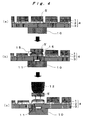
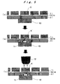
- the cut chip 5' as shown in the cross sectional diagram of Fig. 4(a) is pushed up by pushing-up pins 11 from the back side of the base film 3 of the wafer-dicing adhesive tape 4 as shown in the cross sectional diagram of Fig. 4(b).
- the stress on this occasion is sufficiently introduced to the chip 5' to deform the shape of the tape at the ends of the chip 5'.
- deformation causes a delamination-starting portion 15 of the tape on the ends of the chip 5'.
- the inner removable adhesive layer 2 also contains a radiation-polymerizable compound, so that the temporary adhesion strength can be extensively adjusted so as to cause a delamination-starting portion 15 of the ends of the chip easily. Subsequently, as shown in the cross sectional diagram of Fig. 4(c), the cut chip 5' is picked up by an adsorption collet 12.
- the reference numeral 10 in the drawings refers to an adsorption stage.
- the conventional wafer-dicing adhesive tape is cut completely into the base film thereof in general.
- the base film is molten by the blade, which is being rotated at high speed to be used for cutting, to generate so-called dicing waste in a filamentous form.
- the tape has a constitution such that the removable adhesive layer is laminated on the base film and the generation of dicing waste can be prevented by avoiding the blade to reach to the base film.
- the radiation-polymerizable compound for use in the present invention is appropriately chosen depending on usage without any particular limitation.
- an acrylic resin is preferably used as a base resin.
- examples thereof include an acrylic copolymer and a methacrylic copolymer (hereinafter, also referred to as (meth)acrylic copolymer).
- (meth)acrylic copolymer a methacrylic copolymer
- one appropriately blended with a curing agent and cross-linked before the irradiation with radiation can be used.
- Examples of the (meth)acrylic copolymer include a polymer having a (meth)acrylate as a respective polymer constitutional unit, a (meth)acrylic polymer of a (meth)acrylate-series copolymer, a copolymer with a functional monomer, and mixtures of those polymers.
- Generally applied molecular weights of these polymers may be of higher molecular weights, weight average molecular weights of about 500,000 to 1,000,000.
- the curing agent is used for adjusting temporary adhesive force and cohesive force by reacting with a functional group processed by the (meth)acrylic copolymer.
- the curing agent include: an epoxy compound having two or more epoxy groups in a molecule such as 1,3-bis(N,N-diglycidyl aminomethyl)cyclohexane, 1,3-bis(N,N-diglycidyl aminomethyl) toluene, 1,3-bis(N,N-diglycidyl aminomethyl)benzene, and N,N,N,N'-tetraglycidyl-m-xylenediamine; an isocyanate-based compound having two or more isocyanate groups in a molecule such as 2,4-tolylene diisocyanate, 2,6-tolylene diisocyanate, 1 ,3-xylylene diisocyanate, 1,4-xylene diisocyanate, and diphenylmethane-4,4'-diisocyanate; and an azi
- a low molecular weight compound having at least two or more photopolymerizable carbon-carbon double bonds in a molecule capable of forming three-dimensional network through, for example, irradiation with light is widely used as the radiation-polymerizable compound. It is preferable that an oligomer having a weight average molecular weight (Mw) ranging from 100 to 30,000 be used.
- Mw weight average molecular weight
- An example of such compound can include an oligomer having a functional group such as a hydroxyl group or a carboxyl group, such as a urethane acrylate, epoxy acrylate, polyester acrylate, polyether acrylate, (meth)acrylic oligomer, and itaconic oligomer.
- specific examples of the compound that is applicable include: trimethylolpropane triacrylate, tetramethylolmethane tetraacrylate, pentaerythritol triacrylate, pentaerythritol tetraacrylate, dipentaerythritol monohydroxy pentaacryalte, dipentaerythritol hexaacrylate, 1,4-butyleneglycol diacrylate, 1,6-hexanediol diacrylate, polyethyleneglycol diacrylate, and oligoester acrylate; and urethane acrylate-based oligomers including one obtained by reacting acrylate or methacrylate having a hydroxyl group (for example, 2-hydroxyethyl acrylate, 2-hydroxyethyl methacrylate, 2-hydroxypropyl acrylate, 2-hydroxypropyl methacrylate, polyethyleneglycol acrylate, or polyethyleneglycol methacrylate) with an is
- This radiation-polymerizable compound contains an acrylic polymer having one or more radiation-polymerizable carbon-carbon double bonds on its side chain as a constitutional unit.
- the radiation-polymerizable compound having one or more radiation-polymerizable carbon-carbon double bonds on the side chain is a polymer having a carbon-carbon double bond in its molecule.
- the compound may be obtained by addition polymerization of a compound having one or more carbon-carbon double bonds to a homopolymer having an alkyl ester of acrylic acid or methacrylic acid as a main constitutional unit or to a copolymer of an alkyl ester of acrylic acid or methacrylic acid and another unsaturated monomer copolymerizable therewith.
- this polymer has a weight average molecular weight of 10,000 to 1,000,000, while a glass-transition temperature thereof may be appropriately adjusted by changing the blending ratio of the alkyl ester.
- a urethane acrylate-based oligomer can be used.
- a content of the radiation-polymerizable compound in the resin composition that constitutes the outermost removable adhesive layer is different from that of the inner removable adhesive layer. According to such a constitution, it is possible to provide a difference in the temporary adhesion strength after irradiation with radiation between the outermost removable adhesive layer and the inner removable adhesive layer. In addition, because a stress applied to the base film is sufficiently introduced to the outermost removable adhesive layer irradiated with radiation, it is possible to easily peel off said layer from chips cut.
- the content of the radiation-polymerizable compound in the composition of the outermost removable adhesive layer is determined so to be higher than that of the radiation-polymerizable compound in the composition of the inner removable adhesive layer.
- Such a constitution attains a sufficient reduction in the temporary adhesion strength of the outermost removable adhesive layer to be touched with the chips, when the chips are picked up after irradiation with radiation, to allow the chips to be easily delaminated.
- the inner removable adhesive layer exhibits flexibility and thus the picking up can be carried out without allowing the removable adhesive layers to be delaminated from each other.
- the content of the radiation-polymerizable compound in the composition of the outermost removable adhesive layer 1 is larger than that of the radiation-polymerizable compound in the composition of the inner removable adhesive layer 2; and that the resin composition constituting the outermost removable adhesive layer 1 contains 50 to 200 parts by mass of the radiation-polymerizable compound for 100 parts by mass of the acrylic base resin, and the resin composition constituting the inner removable adhesive layer 2 present in the inner part to the outermost removable adhesive layer 1 contains 5 to 100 parts by mass of the radiation-polymerizable compound for 100 parts by mass of the acrylic base resin.
- the content of the radiation-polymerizable compound in the removable adhesive layer 1 is low, the content of the radiation-polymerizable compound in the removable adhesive layer 2 is high, and the content of the radiation-polymerizable compound in the resin composition constituting the outermost removable adhesive layer is smaller than the content of the radiation-polymerizable compound in the resin composition constituting the inner removable adhesive layer, the decrease in temporary adhesion strength of the outermost removable adhesive layer is insufficient and the inner removable adhesive layer is slightly hard.
- the thus-obtained tape has very bad property of picking up and cannot be developed to a practical level, as well as the expanded diameter of the wafer cannot attain a sufficient level.
- the content of the radiation-polymerizable compound in the resin composition constituting the outermost removable adhesive layer 1 is less than 50 parts by mass, a reduction in temporary adhesion strength is insufficient in some cases, so it becomes difficult to deal with comparatively large chips having a chip size of over 10 mm x 10 mm. Too large content is unfavorable because no additional reduction in temporary adhesive strength may occur while an increase in cost may occur as an opposite effect.
- the content of the radiation-polymerizable compound in the resin composition constituting the inner removable adhesive layer 2 located on the inner side of the outermost removable adhesive layer 1 is less than 5 parts by mass, the content may become a cause of excess flexibility that may lead to a deterioration in property of picking up or may induce the contamination on the back side of the chips in some cases.
- the content is preferably 10 parts by mass or more and further preferably 15 parts by mass or more.
- the content exceeds 100 parts by mass, the composition may become hardened, resulting in leading to deteriorations in properties of picking up and expanding, in some cases.
- a thickness ratio between the outermost removable adhesive layer 1 and the inner removable adhesive layer 2 varies depending on the relationship with the depth of the cutting blade or the compositions. Basically, however, only the peelability of the chips has to be taken into consideration for the outermost removable adhesive layer 1.
- the overall hardness varies depending on the inner removable adhesive layer 2. Therefore, the inner removable adhesive layer 2 is desirably thicker than the outermost removable adhesive layer 1.
- the inner removable adhesive layer 2 has a thickness of preferably 5 to 70 ⁇ m, more preferably 5 to 20 ⁇ m.
- the outermost removable adhesive layer 1 has a thickness of preferably 10 to 80 ⁇ m, more preferably 15 to 50 ⁇ m.
- the two or more removable adhesive layers defined in the present invention does not include removable adhesive layers produced by a method in which after the inner removable adhesive layer 2 has been hardened, the outermost removal adhesive layer 1 is provided.
- a photo-polymerization initiator is used when the removable adhesive layer obtained by means of those adjustments is brought into polymerization or curing through, for example, irradiation with ultraviolet rays or the like.
- the initiator include isopropylbenzoin ether, isobutylbenzoin ether, benzophenone, Michler's ketone, chlorothioxanthone, dodecylthioxanthone, dimethylthioxanthone, diethylthioxanthone, benzyldimethylketal, ⁇ -hydroxycyclohexylphenylketone, and 2-hydroxymethylphenylpropane.
- the base film 3 of the wafer-dicing adhesive tape 4 in the present invention is not specifically limited as far as the irradiation of the resin compositions constituting the removable adhesive layer is not prevented.
- various ethylene-based copolymers such as an ethylene-vinyl acetate copolymer and an ethylene-(meth)acrylate copolymer, and various elastomers, polyesters, and nylon-series can be applied.
- the thickness of the base film 3 to be applied is not particularly limited, but generally in the range of about 30 to 500 ⁇ m in terms of workability and the like.
- a copolymer containing 2-ethylhexyl acrylate, methyl acrylate, and 2-hydroxyethyl acrylate was used.
- a radiation-curable acrylic polymer obtained by addition of 5 parts by mass of 2-isocyanate ethylmethacrylate as a compound having one or more radiation-polymerizable carbon-carbon double bonds to 100 parts by mass of a polymer obtained by copolymerizing butyl acrylate, 2-ethylhexyl acrylate, methyl methacrylate, and 2-hydroxyethyl acrylate was used.
- a removable adhesive agent was obtained by: adding 100 parts by mass of the above acrylic base resin with 3 parts by mass of a polyisocyanate compound (trade name: Colonate L, manufactured by Nippon Polyurethane Industry Co., Ltd.) as a curing agent, predetermined mixing parts of the above radiation-polymerizable compound described in the examples and comparative examples, and 1 part by mass of ⁇ -hydroxycyclohexyl phenylketone as a photo polymerization initiator; and mixing them together.
- a polyisocyanate compound trade name: Colonate L, manufactured by Nippon Polyurethane Industry Co., Ltd.
- a base film of 100 ⁇ m in thickness was prepared by the T-die extrusion method using an EMMA resin (trade name: Acrift WD201, manufactured by Sumitomo Chemical Industrial Co., Ltd.). Subsequently, on the base film, an inner removable adhesive layer (Removable adhesive layer 2) and an outermost removable adhesive layer (Removable adhesive layer 1) having the compositions shown in the examples and comparative examples in Tables 1 and 2 were applied in this order such that the inner removable adhesive layer had a thickness of 35 ⁇ m and the outermost removable adhesive layer had a thickness of 10 ⁇ m, thereby obtaining an wafer-dicing adhesive tape.
- EMMA resin trade name: Acrift WD201, manufactured by Sumitomo Chemical Industrial Co., Ltd.
- the respective wafer-dicing adhesive tapes of the examples and comparative examples in Tables 1 and 2 were applied and fixed on an 8-inch ring frame. While being applied and fixed, an 8-inch silicon wafer of 100 ⁇ m in thickness was applied on the wafer-dicing adhesive tape and then cut into chips of 5 mm x 5 mm in size as full-cut dicing with a dicing machine DAD340 (trade name) manufactured by Disco, Co., Ltd. In this process, the depths of the cutting blade from the tape surface were those represented in Tables 1 and 2, respectively.
- the numbers of filamentous dicing wastes generated from the tape by dicing were counted by microscopical observation. The observation was carried out for five scribing lines.
- the numbers of the powdery cutting wastes generated from the removable adhesive layers by dicing and adhered on the wafer were counted by microscopical observation so that the presence or absence of the wastes was confirmed.
- Chips were actually picked up using CPS-100FM (trade name) manufactured by MEC Machinery Inc. with expand strokes of 2 mm and 12 mm, respectively, so that whether the chips could be pulled up, adsorbed in a circular collet, and mounted on a lead frame was evaluated. The evaluation was conducted in the view how many chips, among 200 chips, were successfully picked up from the 8-inch wafer.
- the expanding rate of the diameters of the wafer (the diameter of the wafer at expanding / the original diameter of the 8-inch wafer), when the wafer was expanded with an expanding stroke of 12 mm, and the presence or absence of breaking of the dicing tape were observed, respectively.
- the diameter of the wafer can be sufficiently expanded at an expanding stroke of 12 mm without causing filamentous dicing waste or fine powdery cutting waste and without any problem in property of picking up.
- the content of the radiation-polymerizable compound of the removable adhesive layer 1 was slightly low, so that the property of picking up was at a lower level. In this case, however, good results were obtained with respect to other items without any problem, just as in the cases of Examples 1 to 3.
- the property of picking up was at a lower level because the content of the radiation-polymerizable compound of the removable adhesive layer 2 was slightly low. In these cases, however, good results were obtained with respect to other items without any problem, just as in the cases of Examples 1 to 3.
- Example 5 because the content of the radiation-polymerizable compound of the removable adhesive layer 2 was slightly high, the layer was hardened after the UV irradiation. Thus, the expanded diameter of the wafer by expanding was not necessarily sufficient. Besides, the property of picking up was at a lower level because the hardened removable layer was expanded at a stroke of 12 mm. In this case, however, good results were obtained with respect to other items without any problem, just as in the cases of Examples 1 to 3.
- Comparative Example 1 the removable adhesive layer 2 was previously hardened by irradiation with radiation. Thus, a large amount of cutting powders was generated from the removable adhesive layer 2 at the time of cutting with the blade and then adhered on the wafer, so that the product of Comparative Example 1 could not be developed to a practical level.
- the removable adhesive layer 2 did not contain a radiation-curable type removable adhesive agent and it was kept in a soft state even after UV irradiation. Therefore, the stress of pushing up by the pushing-up pins upon picking up was absorbed by the soft removable adhesive layer 2, so that the chips could not be picked up at all.
- the removable adhesive layer 1 did not contain a radiation-curable type removable adhesive agent, so that the temporary adhesion strength could not be decreased. As a result, the chips could be hardly picked up. Furthermore, in Comparative Example 4, the content rates of the radiation-polymerizable compound with respect to an acrylic removable adhesive agent in the removable adhesive layer 1 and that in the removable adhesive layer 2 were equal. Besides, the content of the radiation-polymerizable compound itself was high and both layers were hardened too much after the UV irradiation, thereby breaking at scribing line portions with an expanding stroke of 12 mm.
- the wafer-dicing adhesive tape of the present invention can be used for supporting and fixing a work to be cut, such as a wafer, when the work to be cut is subjected to processing. Furthermore, in the method of producing chips using the same, semiconductor chips being advanced with respect to thin thickness and a small size can be efficiently produced without generating cutting waste at the time of dicing.
Landscapes
- Chemical & Material Sciences (AREA)
- Organic Chemistry (AREA)
- Chemical Kinetics & Catalysis (AREA)
- Dicing (AREA)
- Adhesive Tapes (AREA)
- Adhesives Or Adhesive Processes (AREA)
Applications Claiming Priority (2)
| Application Number | Priority Date | Filing Date | Title |
|---|---|---|---|
| JP2005095810 | 2005-03-29 | ||
| PCT/JP2006/306309 WO2006104151A1 (fr) | 2005-03-29 | 2006-03-28 | Bande adhesive pour decoupage en des de tranches et procede de fabrication de puces l’utilisant |
Publications (2)
| Publication Number | Publication Date |
|---|---|
| EP1865545A1 true EP1865545A1 (fr) | 2007-12-12 |
| EP1865545A4 EP1865545A4 (fr) | 2008-03-26 |
Family
ID=37053407
Family Applications (1)
| Application Number | Title | Priority Date | Filing Date |
|---|---|---|---|
| EP06730257A Withdrawn EP1865545A4 (fr) | 2005-03-29 | 2006-03-28 | Bande adhesive pour decoupage en des de tranches et procede de fabrication de puces l utilisant |
Country Status (8)
| Country | Link |
|---|---|
| US (1) | US7985474B2 (fr) |
| EP (1) | EP1865545A4 (fr) |
| JP (1) | JP5019613B2 (fr) |
| KR (1) | KR101058975B1 (fr) |
| CN (1) | CN101138075B (fr) |
| MY (1) | MY147688A (fr) |
| TW (1) | TWI333672B (fr) |
| WO (1) | WO2006104151A1 (fr) |
Cited By (2)
| Publication number | Priority date | Publication date | Assignee | Title |
|---|---|---|---|---|
| EP1930386A3 (fr) * | 2006-12-06 | 2010-04-28 | Nitto Denko Corporation | Composition adhésive sensible à la pression amovible et bande ou feuille adhésive sensible à la pression |
| EP3950226A4 (fr) * | 2019-03-29 | 2022-11-30 | Mitsui Chemicals Tohcello, Inc. | Procédé de production de dispositifs électroniques et de films adhésifs |
Families Citing this family (9)
| Publication number | Priority date | Publication date | Assignee | Title |
|---|---|---|---|---|
| JP5027460B2 (ja) * | 2006-07-28 | 2012-09-19 | 東京応化工業株式会社 | ウエハの接着方法、薄板化方法、及び剥離方法 |
| CN102157422A (zh) * | 2010-02-12 | 2011-08-17 | 古河电气工业株式会社 | 卷芯及卷绕于卷芯的晶片加工用带 |
| JP5641641B2 (ja) * | 2010-07-29 | 2014-12-17 | 日東電工株式会社 | ダイシングテープ一体型半導体裏面用フィルム及び半導体装置の製造方法 |
| CN103370780B (zh) * | 2011-02-18 | 2016-01-20 | 应用材料公司 | 晶片级分割的方法和系统 |
| JP5805411B2 (ja) | 2011-03-23 | 2015-11-04 | ファスフォードテクノロジ株式会社 | ダイボンダのピックアップ方法およびダイボンダ |
| TWI671799B (zh) * | 2011-03-30 | 2019-09-11 | Sumitomo Bakelite Co., Ltd. | 半導體晶圓等加工用黏著帶 |
| JP5770038B2 (ja) * | 2011-07-25 | 2015-08-26 | リンテック株式会社 | 粘着シート |
| CN105143380B (zh) * | 2013-03-28 | 2019-05-17 | 古河电气工业株式会社 | 粘合带及晶片加工用胶带 |
| JP6582013B2 (ja) * | 2017-03-31 | 2019-09-25 | 古河電気工業株式会社 | 剥離ライナー付マスク一体型表面保護テープ |
Family Cites Families (15)
| Publication number | Priority date | Publication date | Assignee | Title |
|---|---|---|---|---|
| US5281473A (en) * | 1987-07-08 | 1994-01-25 | Furakawa Electric Co., Ltd. | Radiation-curable adhesive tape |
| JPH05211234A (ja) | 1991-12-05 | 1993-08-20 | Lintec Corp | ウェハ貼着用粘着シートおよびウェハダイシング方法 |
| US5476566A (en) * | 1992-09-02 | 1995-12-19 | Motorola, Inc. | Method for thinning a semiconductor wafer |
| JPH07235583A (ja) * | 1994-02-24 | 1995-09-05 | Nec Kansai Ltd | 粘着シート |
| JP3388674B2 (ja) * | 1996-04-19 | 2003-03-24 | リンテック株式会社 | エネルギー線硬化型感圧接着剤組成物およびその利用方法 |
| GB2320615B (en) * | 1996-12-19 | 2001-06-20 | Lintec Corp | Process for producing a chip and pressure sensitive adhesive sheet for said process |
| US6312800B1 (en) * | 1997-02-10 | 2001-11-06 | Lintec Corporation | Pressure sensitive adhesive sheet for producing a chip |
| JP4072927B2 (ja) * | 1997-08-28 | 2008-04-09 | リンテック株式会社 | エネルギー線硬化型親水性粘着剤組成物およびその利用方法 |
| JP4510954B2 (ja) * | 1998-08-10 | 2010-07-28 | リンテック株式会社 | ダイシングテープ及びダイシング方法 |
| JP3784202B2 (ja) | 1998-08-26 | 2006-06-07 | リンテック株式会社 | 両面粘着シートおよびその使用方法 |
| JP4947564B2 (ja) * | 2000-01-21 | 2012-06-06 | 日東電工株式会社 | 半導体ウエハ加工用粘着シート |
| JP4392732B2 (ja) * | 2000-02-07 | 2010-01-06 | リンテック株式会社 | 半導体チップの製造方法 |
| JP2003007646A (ja) | 2001-06-18 | 2003-01-10 | Nitto Denko Corp | ダイシング用粘着シートおよび切断片の製造方法 |
| JP2003218063A (ja) * | 2002-01-24 | 2003-07-31 | Canon Inc | ウエハ貼着用粘着シート及び該シートを利用する加工方法 |
| JP4865192B2 (ja) * | 2004-03-16 | 2012-02-01 | 古河電気工業株式会社 | 半導体固定用粘着テープ |
-
2006
- 2006-03-27 TW TW095110530A patent/TWI333672B/zh active
- 2006-03-28 EP EP06730257A patent/EP1865545A4/fr not_active Withdrawn
- 2006-03-28 CN CN200680008106XA patent/CN101138075B/zh not_active Expired - Fee Related
- 2006-03-28 WO PCT/JP2006/306309 patent/WO2006104151A1/fr not_active Ceased
- 2006-03-28 KR KR1020077021652A patent/KR101058975B1/ko not_active Expired - Lifetime
- 2006-03-28 JP JP2007510530A patent/JP5019613B2/ja not_active Expired - Lifetime
- 2006-03-28 MY MYPI20061364A patent/MY147688A/en unknown
-
2007
- 2007-08-28 US US11/892,905 patent/US7985474B2/en not_active Expired - Lifetime
Cited By (3)
| Publication number | Priority date | Publication date | Assignee | Title |
|---|---|---|---|---|
| EP1930386A3 (fr) * | 2006-12-06 | 2010-04-28 | Nitto Denko Corporation | Composition adhésive sensible à la pression amovible et bande ou feuille adhésive sensible à la pression |
| EP2277965A3 (fr) * | 2006-12-06 | 2011-04-13 | Nitto Denko Corporation | Composition adhésive sensible à la pression amovible et bande ou feuille adhésive sensible à la pression |
| EP3950226A4 (fr) * | 2019-03-29 | 2022-11-30 | Mitsui Chemicals Tohcello, Inc. | Procédé de production de dispositifs électroniques et de films adhésifs |
Also Published As
| Publication number | Publication date |
|---|---|
| KR101058975B1 (ko) | 2011-08-23 |
| JP5019613B2 (ja) | 2012-09-05 |
| EP1865545A4 (fr) | 2008-03-26 |
| TW200641987A (en) | 2006-12-01 |
| TWI333672B (en) | 2010-11-21 |
| MY147688A (en) | 2012-12-31 |
| US20080008881A1 (en) | 2008-01-10 |
| JPWO2006104151A1 (ja) | 2008-09-11 |
| CN101138075B (zh) | 2011-04-20 |
| KR20070118094A (ko) | 2007-12-13 |
| CN101138075A (zh) | 2008-03-05 |
| US7985474B2 (en) | 2011-07-26 |
| WO2006104151A1 (fr) | 2006-10-05 |
Similar Documents
| Publication | Publication Date | Title |
|---|---|---|
| US7985474B2 (en) | Wafer-dicing adhesive tape and method of producing chips using the same | |
| JP5064985B2 (ja) | 半導体ウェハの処理方法 | |
| US8389629B2 (en) | Adhesive, adhesive sheet, multi-layered adhesive sheet, and production method for electronic part | |
| JP3784202B2 (ja) | 両面粘着シートおよびその使用方法 | |
| CN113675131B (zh) | 半导体芯片的制造方法和用于该制造方法的掩模一体型表面保护带 | |
| JP7042667B2 (ja) | 半導体チップの製造方法 | |
| US7105226B2 (en) | Pressure sensitive adhesive double coated sheet and method of use thereof | |
| KR102188284B1 (ko) | 마스크 일체형 표면 보호 테이프 | |
| US11282736B2 (en) | Mask-integrated surface protective tape with release liner | |
| JP5603453B1 (ja) | 半導体ウェハ保護用粘着テープ | |
| JP6800213B2 (ja) | マスク一体型表面保護テープ | |
| KR102294737B1 (ko) | 반도체 칩의 제조 방법 | |
| JP5583080B2 (ja) | ウエハ加工用テープおよびそれを用いた半導体加工方法 | |
| JP4234630B2 (ja) | 貫通構造を有する薄膜化回路基板の製造方法と保護用粘着テープ | |
| JP4128843B2 (ja) | 半導体チップ製造方法 | |
| KR100555995B1 (ko) | 웨이퍼의 제조방법과 점착테이프 | |
| WO2017179439A1 (fr) | Bande adhésive pour le traitement de semi-conducteurs et procédé de fabrication de puce semi-conductrice ou d'élément semi-conducteur l'utilisant | |
| JP2006286900A (ja) | チップの製造方法 | |
| JP2002064131A (ja) | チップ状部品の剥離方法 | |
| JP2011258636A (ja) | ウエハダイシング加工用粘着テープ |
Legal Events
| Date | Code | Title | Description |
|---|---|---|---|
| PUAI | Public reference made under article 153(3) epc to a published international application that has entered the european phase |
Free format text: ORIGINAL CODE: 0009012 |
|
| 17P | Request for examination filed |
Effective date: 20070828 |
|
| AK | Designated contracting states |
Kind code of ref document: A1 Designated state(s): DE IT PT |
|
| A4 | Supplementary search report drawn up and despatched |
Effective date: 20080225 |
|
| RIC1 | Information provided on ipc code assigned before grant |
Ipc: C09J 7/02 20060101ALI20061024BHEP Ipc: H01L 21/68 20060101AFI20080219BHEP Ipc: C09J 4/02 20060101ALI20061024BHEP |
|
| RBV | Designated contracting states (corrected) |
Designated state(s): DE IT PT |
|
| DAX | Request for extension of the european patent (deleted) | ||
| 17Q | First examination report despatched |
Effective date: 20080808 |
|
| GRAP | Despatch of communication of intention to grant a patent |
Free format text: ORIGINAL CODE: EPIDOSNIGR1 |
|
| STAA | Information on the status of an ep patent application or granted ep patent |
Free format text: STATUS: THE APPLICATION HAS BEEN WITHDRAWN |
|
| 18W | Application withdrawn |
Effective date: 20121011 |